
Nominalization of Split DC Link Voltage Dynamics in Three-Phase Three-Level Converters Operating Under Arbitrary Power Factor with Restricted Zero-Sequence Component


Abstract
1. Introduction
2. Materials and Methods
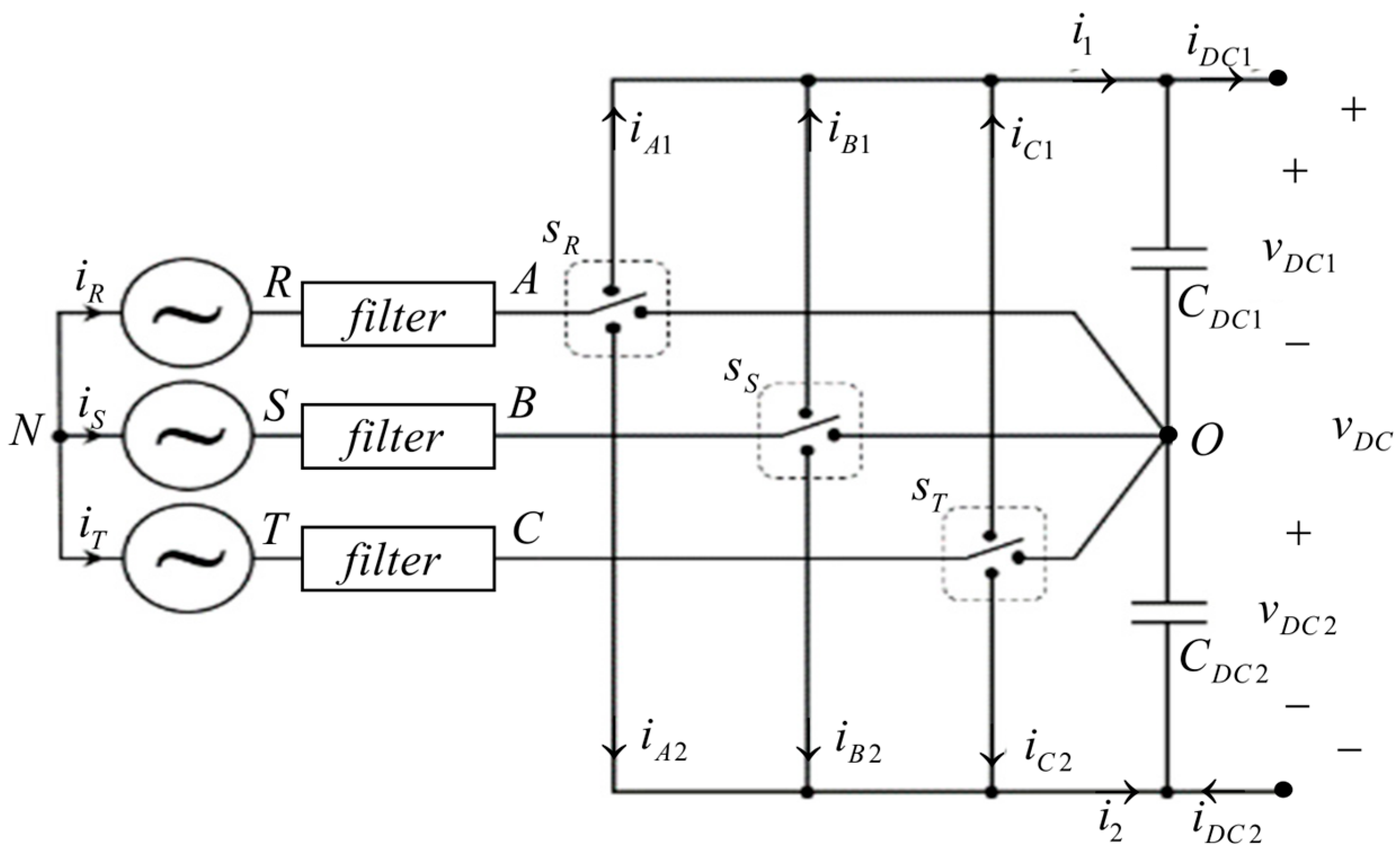
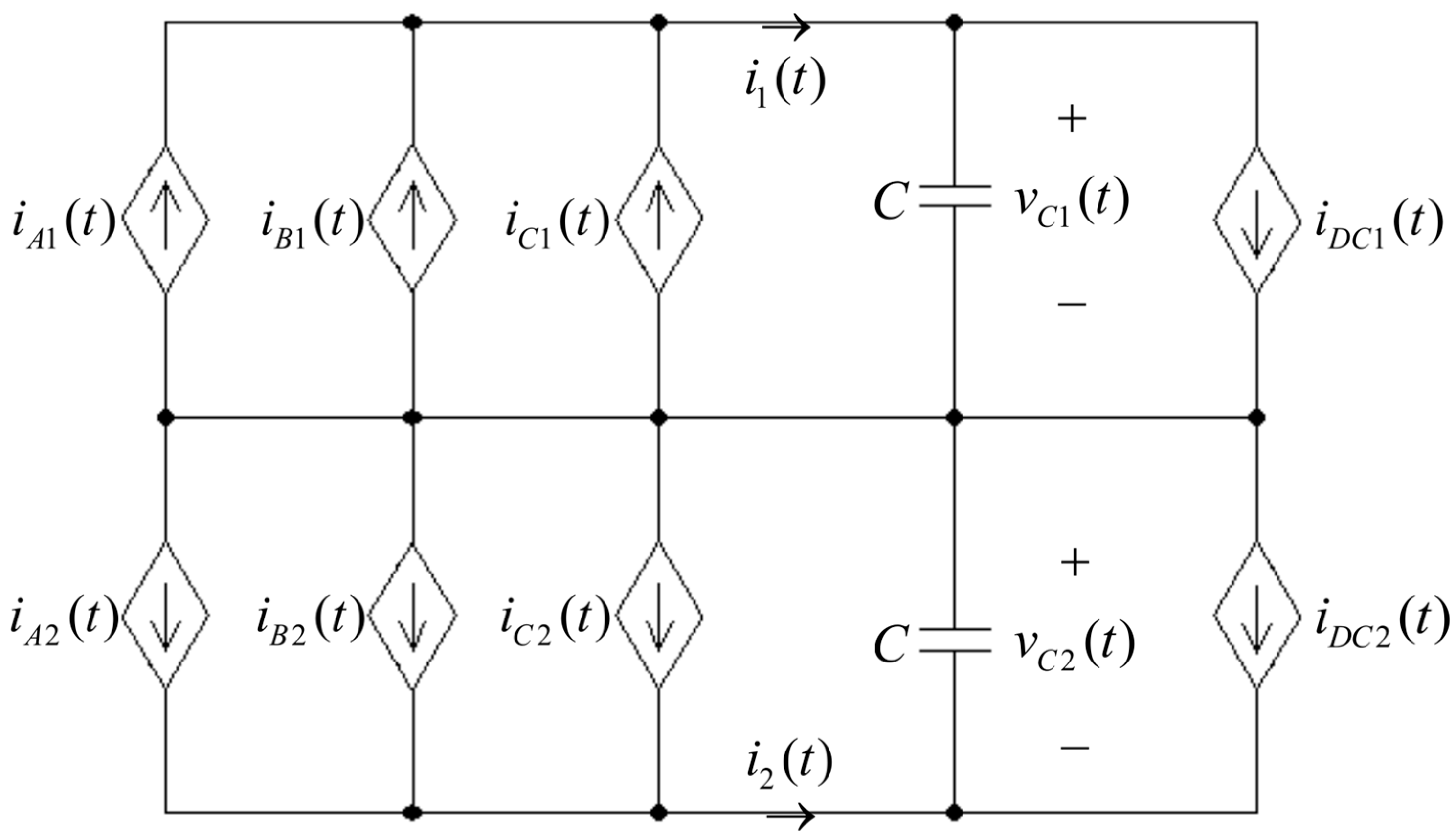
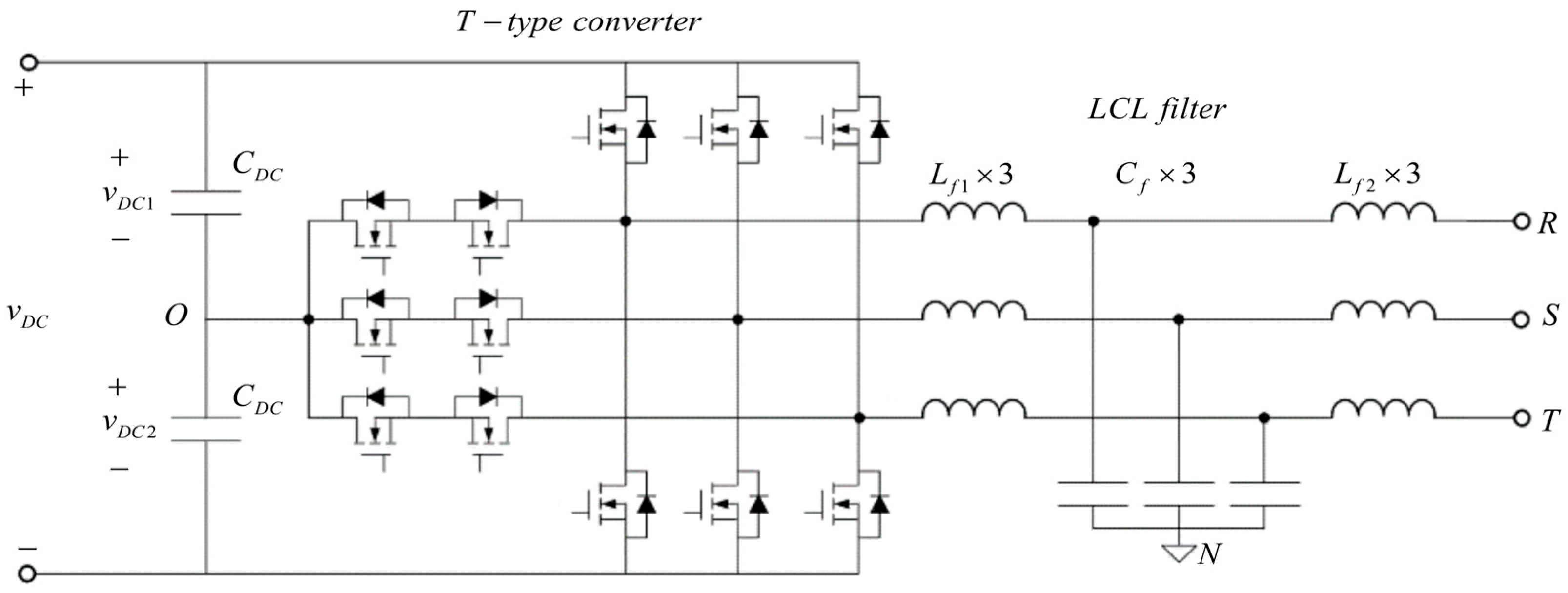
2.1. Converter Under Study
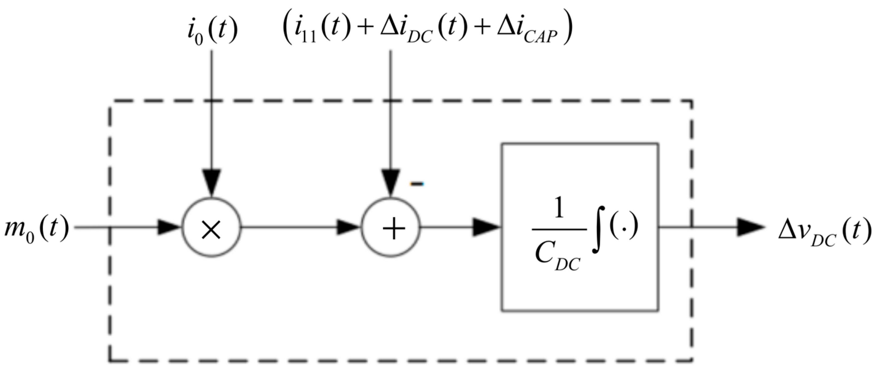
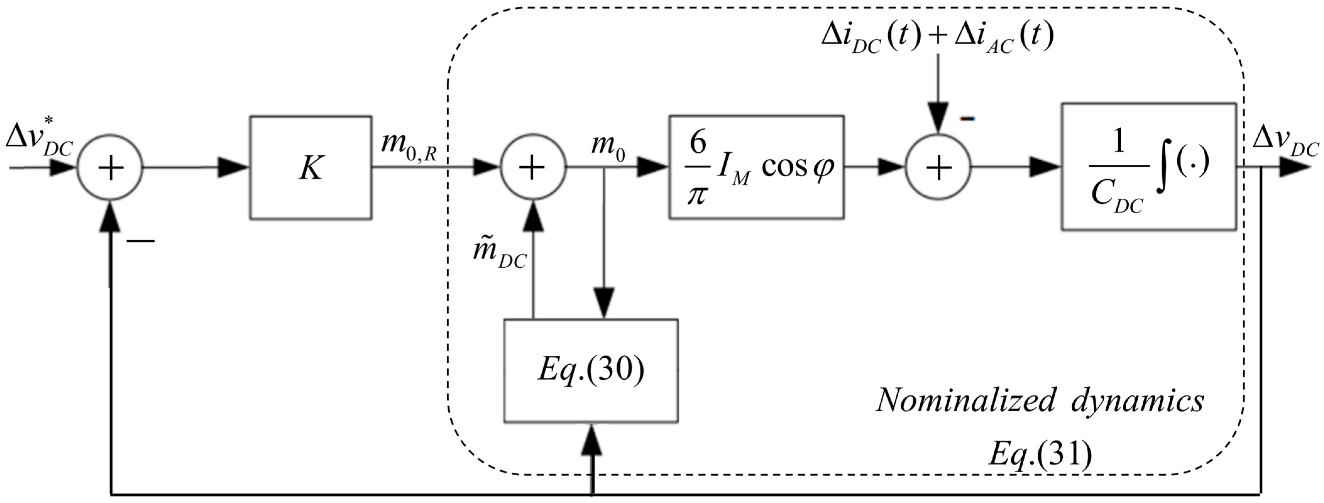
- In case the zero-sequence component m0(t) only contains a DC component in a steady state, only a DC component of i0(t) (i.e., i0,DC in (15)) should be considered as the control gain.
- The current i11(t) contains no DC component in a steady state; hence, it cannot be counteracted by m0(t).
- A non-zero ΔiDC reflects an unbalanced partial DC link loading, given in a steady state by
- 4.
- In an AC-side balanced three-phase system, the total DC link voltage is constant in a steady state [26]. Therefore, ΔiCAP (cf. (11)) is expected to be zero in a steady state and does not have to be treated by m0(t).
2.2. Partial DC Link Voltage Equalization Problem
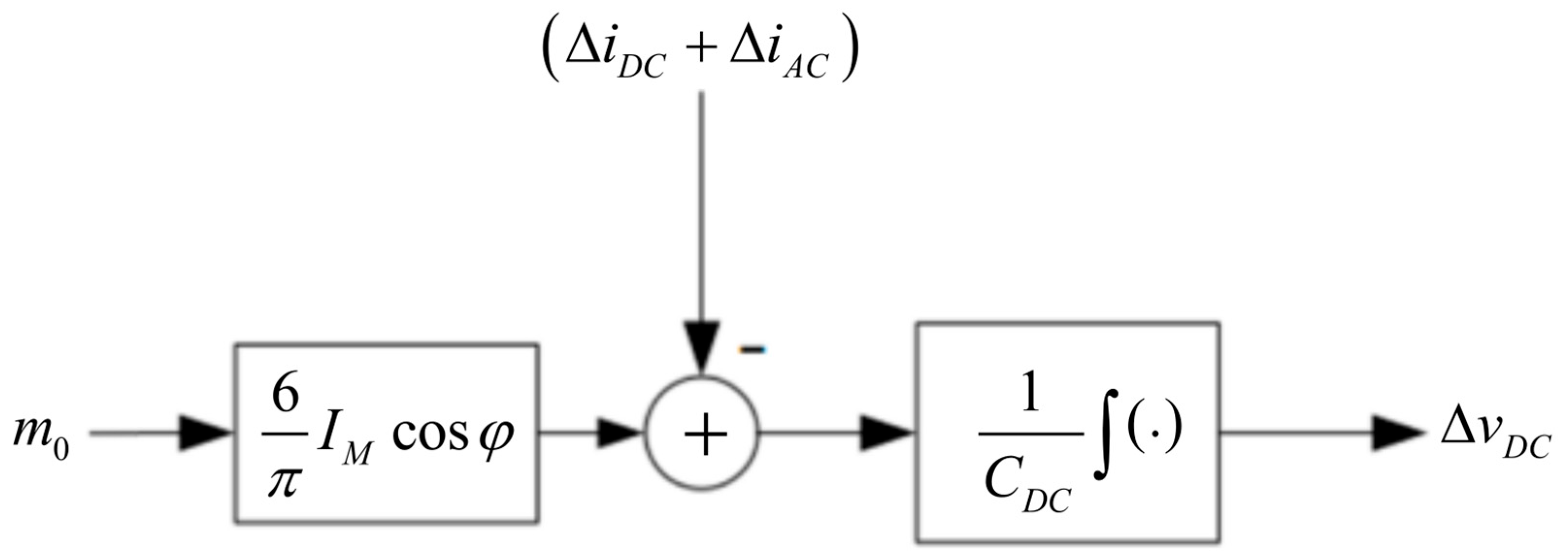
2.3. Disturbance-Observer-Based Nominalization
- -
- Non-causality;
- -
- Noisy derivative action;
- -
- Unknown mAC(t).
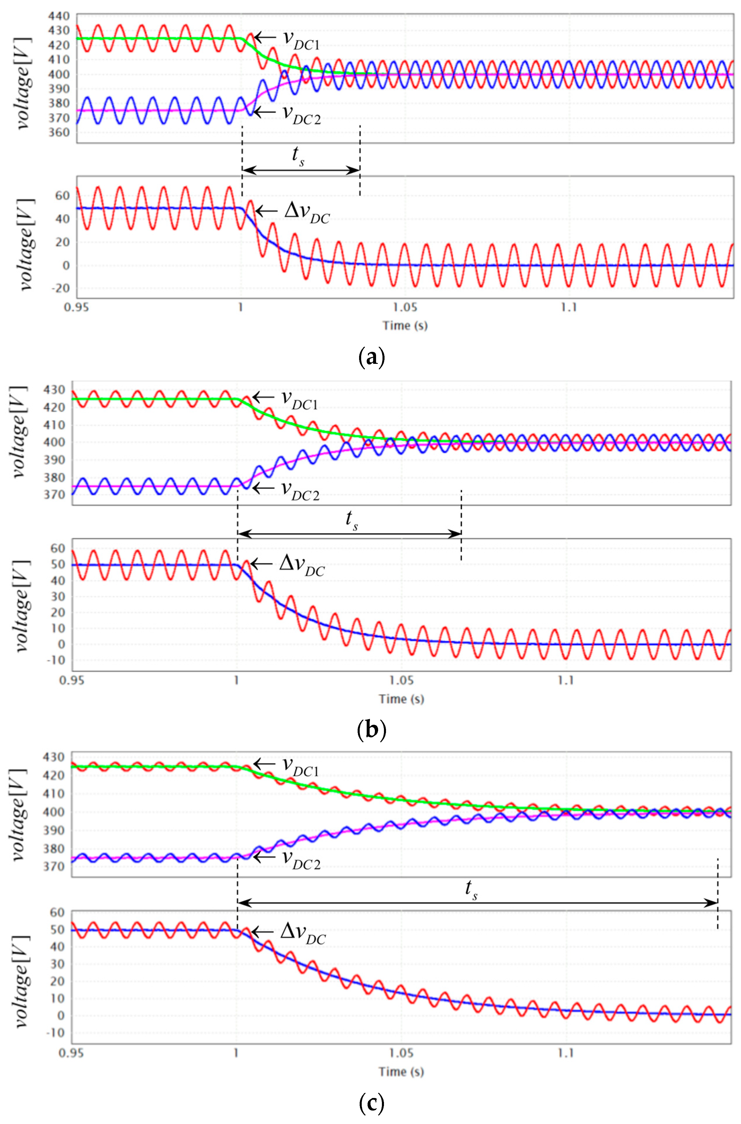
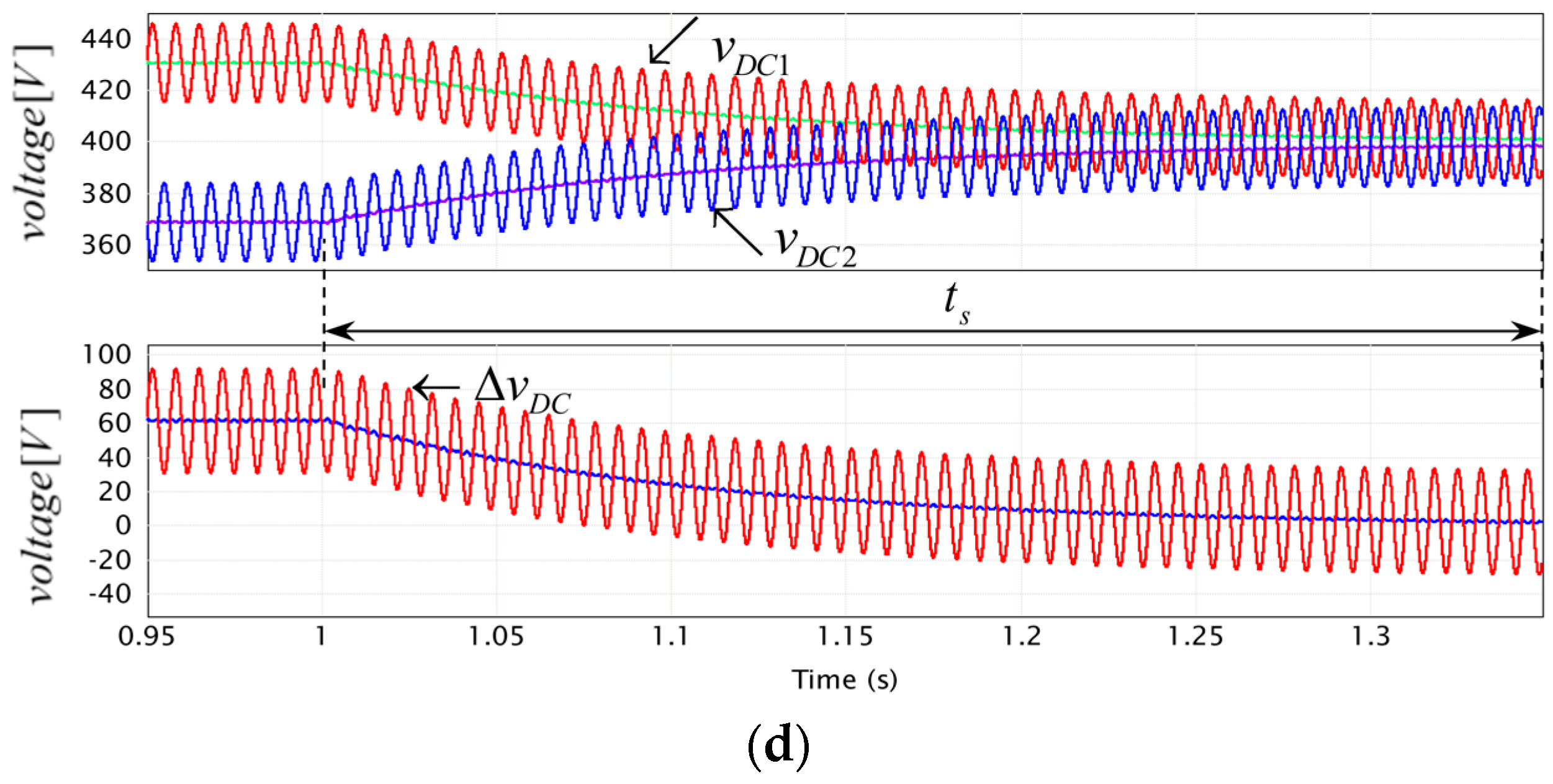
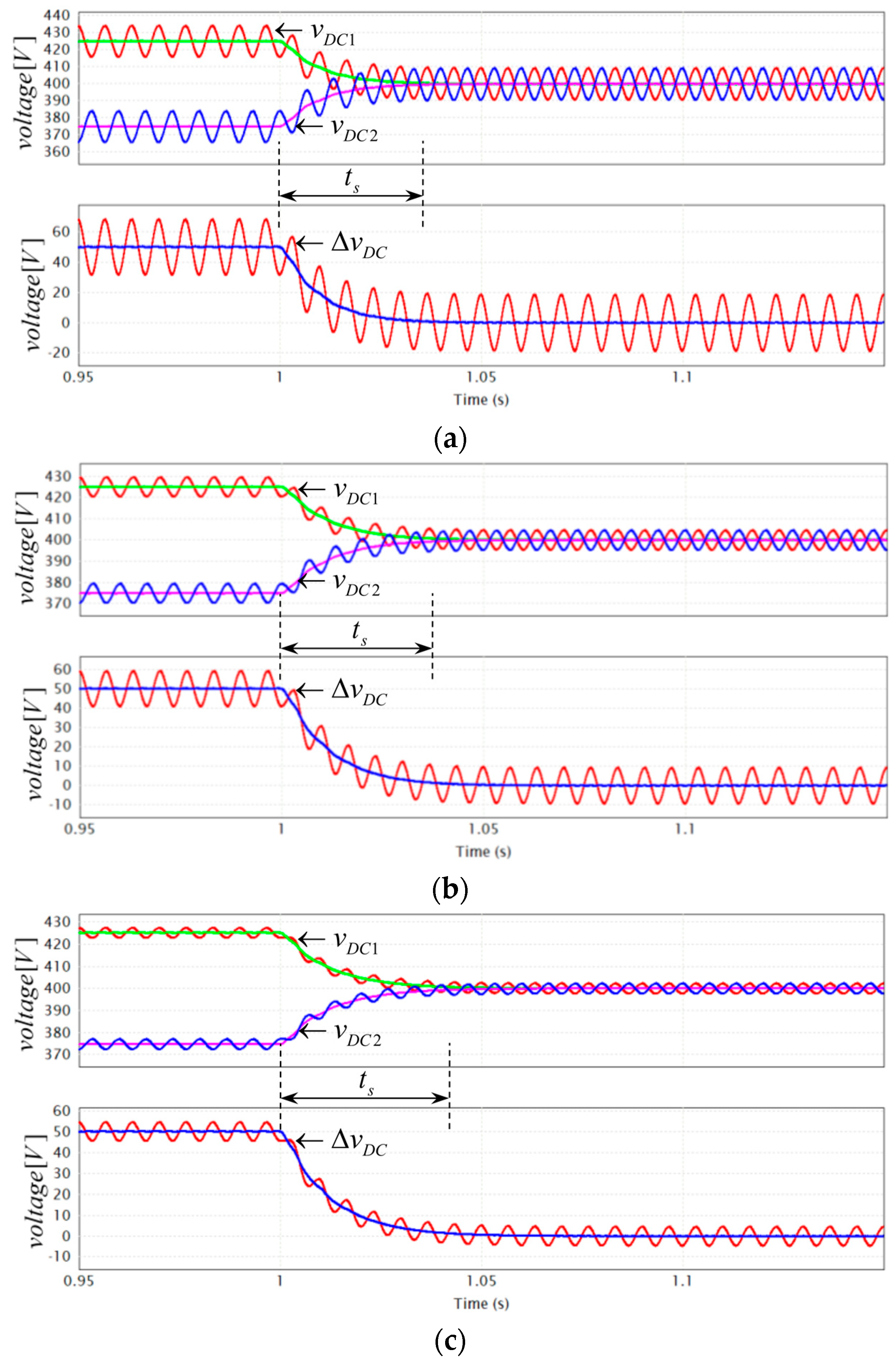
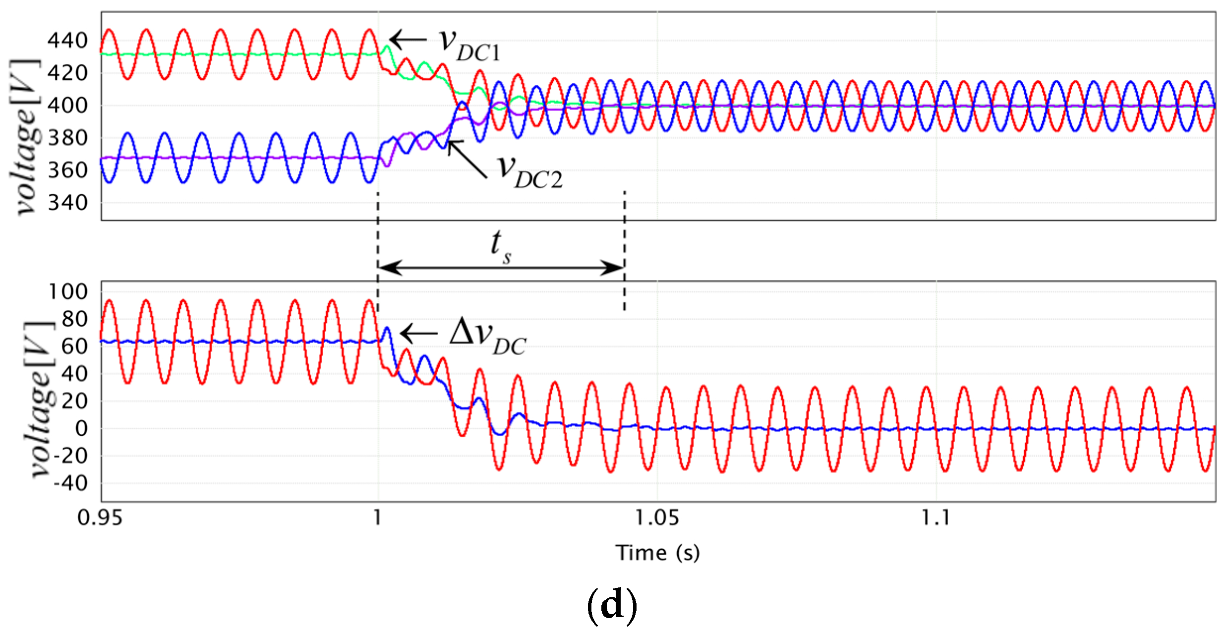
3. Example
4. Discussion
5. Conclusions
Author Contributions
Funding
Data Availability Statement
Conflicts of Interest
Nomenclature
| split DC link capacitances | |
| average DC link capacitance | |
| power factor | |
| average DC link capacitance mismatch | |
| vector of grid currents | |
| grid currents magnitude | |
| unbalanced partial load current | |
| DC component of | |
| AC component of | |
| AC component of disturbance current | |
| vector of modulation indices | |
| zero-sequence modulation component | |
| vector of grid voltages | |
| grid voltages magnitude | |
| partial DC link voltages | |
| sum and difference of partial DC link voltages | |
| convergence time constant | |
| crossover frequency |
References
- Rodriguez, J.; Lai, J.-S.; Peng, F.Z. Multilevel inverters: A survey of topologies, controls, and applications. IEEE Trans. Ind. Electron. 2002, 49, 724–738. [Google Scholar] [CrossRef]
- Barresi, M.; De Simone, D.; Piegari, L.; Baquero, R.S.; Toscani, N. Dual motor drive system based on distributed battery pack modular multilevel converter. IEEE Trans. Power Electron. 2025, 1–16. [Google Scholar] [CrossRef]
- Rodriguez, J.; Bernet, S.; Wu, B.; Pontt, J.O.; Kouro, S. Multilevel voltage-source-converter topologies for industrial medium-voltage drives. IEEE Trans. Ind. Electron. 2007, 6, 2930–2945. [Google Scholar] [CrossRef]
- Barbie, E.; Kuperman, A.; Baimel, D. Current-THD minimization in multilevel inverters with variable DC ratios utilizing a generic closed-form analytic formulation of line-voltage WTHD. Alex. Eng. J. 2023, 66, 211–239. [Google Scholar] [CrossRef]
- Barresi, M.; De Simone, D.; Piegari, L. Direct state-of-charge balancing control for modular multilevel converter integrating batteries. IEEE J. Emerg. Sel. Top. Power Electron. 2025, 13, 733–746. [Google Scholar] [CrossRef]
- Tebrack, C.; Speer, S.; Endish, C. Control and implementation of the parallel enhanced commutation integrated nested multilevel inverter topology. Electronics 2023, 12, 3130. [Google Scholar] [CrossRef]
- Baig, M.A.; Kashif, S.A.R.; Khan, I.A.; Abbas, G. Quick search algorithm-based direct model predictive control of grid-connected 289-level multilevel inverter. Electronics 2023, 12, 3312. [Google Scholar] [CrossRef]
- Barbie, E.; Baimel, D.; Kuperman, A. Frequency spectra based approach to analytical formulation and minimization of voltage THD in staircase modulated multilevel inverters. Alex. Eng. J. 2022, 61, 7781–7809. [Google Scholar] [CrossRef]
- Barresi, M.; Ferri, E.; Piegari, L. A fast charging station for electric vehicles with 400-V/800-V charging ports and second-life batteries. In Proceedings of the 2023 IEEE 17th International Conference on Compatibility, Power Electronics and Power Engineering (CPE-POWERENG), Tallinn, Estonia, 14–16 June 2023; pp. 1–8. [Google Scholar]
- Kwak, J.; Castellazzi, A. State-of-the-art 800V electric drive systems: Inverter-machine co-design for energy efficiency optimization. Electronics 2023, 12, 3063. [Google Scholar] [CrossRef]
- Kim, H.-J.; Park, Y.-M.; Son, Y.-D.; Kang, J.-B.; Lee, J.-Y.; Kim, J.-M. The DC inductor current ripple reduction method for a two-stage power conversion system. Electronics 2023, 12, 3005. [Google Scholar] [CrossRef]
- Anderson, J.A.; Schrittwieser, L.; Leibl, M.; Kolar, J.W. Multi-level topology evaluation for ultra-efficient three-phase inverters. In Proceedings of the 2017 IEEE International Telecommunications Energy Conference (INTELEC), Broadbeach, QLD, Australia, 22–26 October 2017; pp. 456–463. [Google Scholar]
- Schweizer, M.; Friedli, T.; Kolar, J.W. Comparative evaluation of advanced three-phase three-level inverter/converter topologies against two-level systems. IEEE Trans. Ind. Electron. 2013, 60, 5515–5527. [Google Scholar] [CrossRef]
- Stecca, M.; Soeiro, T.B.; Elizondo, L.R.; Bauer, P.; Palensky, P. Comparison of two and three-level DC-AC converters for a 100 kW battery energy storage system. In Proceedings of the 2020 IEEE 29th International Symposium on Industrial Electronics (ISIE), Delft, The Netherlands, 17–19 June 2020; pp. 677–682. [Google Scholar]
- Madan, A.; Bostanci, E. Comparison of two-level and three-level NPC inverter topologies for a PMSM drive for electric vehicle applications. In Proceedings of the 2019 International Aegean Conference on Electrical Machines and Power Electronics (ACEMP) & 2019 International Conference on Optimization of Electrical and Electronic Equipment (OPTIM), Istanbul, Turkey, 27–29 August 2019; pp. 147–154. [Google Scholar]
- Annoukoubi, M.; Essadki, A.; Laghridat, H.; Nasser, T. Comparative study between the performances of a three-level and two-level converter for a wind energy conversion system. In Proceedings of the 2019 International Conference on Wireless Technologies, Embedded and Intelligent Systems (WITS), Fez, Morocco, 3–4 April 2019; pp. 1–6. [Google Scholar]
- Younis, T.; Ibrahim, A.A.; Mattavelli, P. Comparison between two-level and three-level based multi-port converter for interconnected MVAC microgrids. In Proceedings of the IECON 2021—47th Annual Conference of the IEEE Industrial Electronics Society, Toronto, ON, Canada, 13–16 October 2021; pp. 1–6. [Google Scholar]
- Teichmann, R.; Bernet, S. A comparison of three-level converters versus two-level converters for low-voltage drives traction and utility applications. IEEE Trans. Ind. Appl. 2005, 41, 855–865. [Google Scholar] [CrossRef]
- Schweizer, M.; Lizama, I.; Friedli, T.; Kolar, J.W. Comparison of the chip area usage of 2-level and 3-level voltage source converter topologies. In Proceedings of the IECON 2010—36th Annual Conference on IEEE Industrial Electronics Society, Glendale, AZ, USA, 7–10 November 2010; pp. 391–396. [Google Scholar]
- Maheshwari, R.; Munk-Nielsen, S.; Busquets-Monge, S. EMI performance comparison of two-level and three-level inverters in small dc-link capacitors based motor drives. In Proceedings of the 2012 IEEE International Symposium on Industrial Electronics, Hangzhou, China, 28–31 May 2012; pp. 652–657. [Google Scholar]
- Orfanoudakis, G.I.; Sharkh, S.M.; Yuratich, M.A.; Abusara, M.A. Loss comparison of two and three-level inverter topologies. In Proceedings of the 5th IET International Conference on Power Electronics, Machines and Drives (PEMD 2010), Brighton, UK, 19–21 April 2010; pp. 1–6. [Google Scholar]
- Pou, J.; Pindado, R.; Boroyevich, D.; Rodriguez, P. Evaluation of the low-frequency neutral-point voltage oscillations in the three-level inverter. IEEE Trans. Ind. Electron. 2005, 52, 1582–1588. [Google Scholar] [CrossRef]
- Gopalakrishnan, K.S.; Janakiraman, S.; Das, S.; Narayanan, G. Analytical evaluation of DC capacitor RMS current and voltage ripple in neutral-point clamped inverters. Sadhana 2017, 42, 827–839. [Google Scholar] [CrossRef]
- Siton, Y.; Sitbon, M.; Aharon, I.; Lineykin, S.; Baimel, D.; Kuperman, A. On the minimum value of split DC link capacitances in three-phase three-level grid-connected converters operating with unity power factor with limited zero-sequence injection. Electronics 2023, 12, 1994. [Google Scholar] [CrossRef]
- Orfanoudakis, G.I.; Yuratich, M.A.; Sharkh, S.M. Analysis of dc-link capacitor current in three-level neutral point clamped and cascaded H-bridge inverters. IET Power Electron. 2013, 6, 1376–1389. [Google Scholar] [CrossRef]
- Siton, Y.; Yuhimenko, V.; Baimel, D.; Kuperman, A. Baseline for split DC-link design in three-phase three-level converters operating with unity power factor based on low-frequency partial voltage oscillations. Machines 2022, 10, 722. [Google Scholar] [CrossRef]
- Lee, K.-J. Analytical modeling of neutral point current in T-type three-level PWM converter. Energies 2020, 13, 1324. [Google Scholar] [CrossRef]
- Zielinski, C.; Stefanczak, B.; Jedrus, K. Phase-independent reactive power compensation based on four-wire power converter in the presence of angular asymmetry between voltage vectors. Energies 2022, 15, 497. [Google Scholar] [CrossRef]
- Schechter, N.; Kuperman, A. Zero sequence manipulation to maintain correct operation of NPC-PFC rectifier upon neutral line disconnection and reconnection. IEEE Trans. Ind. Electron. 2017, 64, 866–872. [Google Scholar] [CrossRef]
- Lee, K.-J. Analysis of allowable unbalanced load conditions for T-type three-level PWM converter. Energies 2021, 14, 5969. [Google Scholar] [CrossRef]
- Xiao, H.; Xie, S. Leakage current analytical model and application in single-phase transformer-less photovoltaic grid-connected inverter. IEEE Trans. Elecromagnet. Compat. 2010, 52, 902–913. [Google Scholar] [CrossRef]
- Lopez, O.; Freijedo, F.D.; Yepes, A.G.; Fernandez-Comesana, P.; Malvar, J.; Teodorescu, R.; Doval-Gandoy, J. Eliminating ground current in a transformer-less photovoltaic application. IEEE Trans. Energy Convers. 2010, 25, 140–147. [Google Scholar] [CrossRef]
- Lai, R.; Wang, F.; Burgos, R.; Boroyevich, D.; Jiang, D.; Zhang, D. Average modeling and control design for VIENNA-type rectifiers considering the DC-link voltage balance. IEEE Trans. Power Electron. 2009, 24, 2509–2521. [Google Scholar]
- Siton, Y.; Kuperman, A. Generalized analysis of partial DC link voltages behavior in three-phase three-level converters operating with arbitrary power factor with restricted zero-sequence component. Electronics 2023, 12, 4063. [Google Scholar] [CrossRef]
- Siton, Y.; Yuhimenko, V.; Kolesnik, S.; Yahalom, A.; Sitbon, M.; Kuperman, A. Sizing the split DC link capacitance in three-phase three-level bidirectional AC-DC converters operating with arbitrary power factor under zero-sequence injection restriction. Appl. Sci. 2025, 15, 3159. [Google Scholar] [CrossRef]
- Vule, Y.; Siton, Y.; Kuperman, A. Comprehensive modeling and formulation of split DC link capacitors balancing problem in three-phase three-level bidirectional AC/DC converters operating with arbitrary power factor. Alex. Eng. J. 2023, 83, 195–211. [Google Scholar] [CrossRef]
- Kuperman, A.; Horen, Y.; Tapuchi, S. Input-output nominalization of linear systems with slow varying uncertainties. COMPEL—Int. Jour. Comp. Math. Electr. Electron. Eng. 2010, 29, 72–89. [Google Scholar] [CrossRef]
- Huang, Y.; Zhao, M.; Wang, Y.; Zhang, H.; Lu, M. An improved full-speed domain sensorless control scheme for permanent magnet synchronous motor based on hybrid position observer and disturbance rejection optimization. Electronics 2023, 12, 3759. [Google Scholar] [CrossRef]
- Sui, B.; Zhang, J.; Li, Y.; Zhang, Y.; Liu, Z. Fixed-time formation tracking control of multiple unmanned surface vessels considering lumped disturbances and input saturation. Electronics 2023, 12, 3556. [Google Scholar] [CrossRef]
- Sitbon, M.; Schacham, S.; Kuperman, A. Disturbance observer-based voltage regulation of current-mode-boost-converter-interfaced photovoltaic generator. IEEE Trans. Ind. Electron. 2015, 62, 5776–5785. [Google Scholar] [CrossRef]
- Yang, H.; Long, H.; Zhang, Q.; Sun, X. A robust CCS predictive current control for photovoltaic energy storage system based on a nonlinear disturbance observer. Electronics 2023, 12, 1985. [Google Scholar] [CrossRef]
- Alshek, N.; Bronshtein, S.; Elkayam, M.; Kuperman, A. Modified uncertainty and disturbance estimator for enhanced periodic signals suppression. IEEE Trans. Ind. Electron. 2019, 66, 1246–1254. [Google Scholar] [CrossRef]
- Hu, X.; Han, S.; Liu, Y.; Wang, H. Two-axis optoelectronic stabilized platform based on active disturbance rejection controller with LuGre friction model. Electronics 2023, 12, 1261. [Google Scholar] [CrossRef]
- Vule, Y.; Elkayam, M.; Kuperman, A. Uncertainty and disturbance estimator with improved steady-state performance for grid-connected power converters. IET Renew. Power Gen. 2020, 14, 2183–2191. [Google Scholar] [CrossRef]
- Toor, W.A.; Ashraf, M. Performance analysis of learning-based disturbance observer for pulsed superconducting cavity field control. Electronics 2023, 12, 1556. [Google Scholar] [CrossRef]
- Fang, Q.; Zhou, Y.; Ma, S.; Zhang, C.; Wang, Y.; Huangfu, H. Electromechanical actuator servo control technology based on active disturbance rejection control. Electronics 2023, 12, 1934. [Google Scholar] [CrossRef]
- Vule, Y.; Kuperman, A. Plug-in disturbance observer assisted DC link voltage control of grid-connected converters to improve transient performance without deteriorating grid current quality. Int. J. Electr. Power Energy Syst. 2022, 143, 108439. [Google Scholar] [CrossRef]
- Sui, B.; Zhang, J.; Li, Y.; Liu, Y.; Zhang, Y. Fixed-time trajectory tracking control of unmanned surface vessels with prescribed performance constraints. Electronics 2023, 12, 2866. [Google Scholar] [CrossRef]
- Vule, Y.; Kuperman, A. Fast and robust DC Link voltage control of single-phase grid-connected converters supporting 50Hz and 60Hz mains with universal magnitudes range. Int. J. Electr. Power Energy Syst. 2023, 154, 109430. [Google Scholar] [CrossRef]
- Ndabarushimana, E.; Ma, L. Robust sensor fault detection for a single-phase pulse width modulation rectifier. Electronics 2023, 12, 2366. [Google Scholar] [CrossRef]
- Li, Q.; Ding, B. Design of backstepping sliding mode control for a polishing pneumatic system based on extended state observer. Machines 2023, 11, 904. [Google Scholar] [CrossRef]
- Borafker, S.; Strajnikov, P.; Kuperman, A. Design of dual-notch-filter-based controllers for enhancing the dynamic response of universal single-phase grid-connected power converters. Appl. Sci. 2023, 13, 10144. [Google Scholar] [CrossRef]


| cosφ | ts [ms] | |
|---|---|---|
| 1 | 35 | |
| 1 | 70 | |
| 1 | 140 | |
| 1 | 350 | |
| 0.5 | 70 | |
| 0.25 | 140 | |
| 0.1 | 350 |
Disclaimer/Publisher’s Note: The statements, opinions and data contained in all publications are solely those of the individual author(s) and contributor(s) and not of MDPI and/or the editor(s). MDPI and/or the editor(s) disclaim responsibility for any injury to people or property resulting from any ideas, methods, instructions or products referred to in the content. |
© 2025 by the authors. Licensee MDPI, Basel, Switzerland. This article is an open access article distributed under the terms and conditions of the Creative Commons Attribution (CC BY) license (https://creativecommons.org/licenses/by/4.0/).
Share and Cite
Vule, Y.; Kuperman, A. Nominalization of Split DC Link Voltage Dynamics in Three-Phase Three-Level Converters Operating Under Arbitrary Power Factor with Restricted Zero-Sequence Component. Electronics 2025, 14, 2524. https://doi.org/10.3390/electronics14132524
Vule Y, Kuperman A. Nominalization of Split DC Link Voltage Dynamics in Three-Phase Three-Level Converters Operating Under Arbitrary Power Factor with Restricted Zero-Sequence Component. Electronics. 2025; 14(13):2524. https://doi.org/10.3390/electronics14132524
Chicago/Turabian StyleVule, Yan, and Alon Kuperman. 2025. "Nominalization of Split DC Link Voltage Dynamics in Three-Phase Three-Level Converters Operating Under Arbitrary Power Factor with Restricted Zero-Sequence Component" Electronics 14, no. 13: 2524. https://doi.org/10.3390/electronics14132524
APA StyleVule, Y., & Kuperman, A. (2025). Nominalization of Split DC Link Voltage Dynamics in Three-Phase Three-Level Converters Operating Under Arbitrary Power Factor with Restricted Zero-Sequence Component. Electronics, 14(13), 2524. https://doi.org/10.3390/electronics14132524