Article

Optoelectronic Memristor Based on ZnO/Cu2O for Artificial Synapses and Visual System

1
College of Physics, Sichuan University, Chengdu 610065, China
2
College of Mechanical Engineering, Guizhou University of Engineering Science, Bijie 551700, China
*
Author to whom correspondence should be addressed.
Electronics 2025, 14(12), 2490; https://doi.org/10.3390/electronics14122490
Submission received: 22 May 2025 / Revised: 12 June 2025 / Accepted: 18 June 2025 / Published: 19 June 2025

Abstract

:
The development of artificial intelligence has resulted in significant challenges to conventional von Neumann architectures, including the separation of storage and computation, and power consumption bottlenecks. The new generation of brain-like devices is accelerating its evolution in the direction of high-density integration and integrated sensing, storage, and computing. The structural and information transmission similarity between memristors and biological synapses signifies their unique potential in sensing and memory. Therefore, memristors have become potential candidates for neural devices. In this paper, we have designed an optoelectronic memristor based on a ZnO/Cu2O structure to achieve synaptic behavior through the modulation of electrical signals, demonstrating the recognition of a dataset by a neural network. Furthermore, the optical synaptic functions, such as short-term/long-term potentiation and learn-forget-relearn behavior, and advanced synaptic behavior of optoelectronic modulation, are successfully simulated. The mechanism of light-induced conductance enhancement is explained by the barrier change at the interface. This work explores a new pathway for constructing next-generation optoelectronic synaptic devices, which lays the foundation for future brain-like visual chips and intelligent perceptual devices.

1. Introduction

Studies have shown that more than 80% of the perceptual information acquired by humans from the outside world is accomplished through visual perception, which is higher than the sum of the inputs from the other perceptual organs [1]. Thus, building artificial visual systems has been the focus of researchers’ work. Conventional artificial vision systems are composed of three fundamental components: a visual sensing unit, an information processing unit, and a storage unit. They are physically separated from each other [2]. The information captured by the visual sensors is first converted into digital signals, temporarily stored in memory, and then transmitted to the processing unit for pattern recognition. Therefore, the construction of devices with both sensing and memory characteristics is the focus of next-generation artificial vision systems [3,4,5,6].
The memristor is widely recognized as an ideal candidate for the new generation of synaptic devices due to the high similarity of its structure and information processing mechanism with biological synapses [7]. Synapses, as an important part of biological neurons, to implement synaptic functions with hardware devices and then apply devices to synaptic circuit design, have been the focus of researchers. The first memristor was fabricated in HP Labs in 2008; before then, memristors existed only in theory [8]. The conductance of the memristor can be regarded as synaptic weights and can be modulated with external signals. The creation of physical memristors has pushed the development of synaptic devices.
The memristor is usually a metal-insulator-metal (MIM) structure; the top electrode, the functional layer, and the bottom electrode correspond to the presynaptic membrane, the synaptic gap, and the postsynaptic membrane of the biological synapse, respectively. When an external signal is applied to the memristor, it can simulate the biological synapses through its special way of resistance conversion [9]. Initially, memristors were usually modulated using electrical signals. Although memristors have gained the attention of researchers in recent years, issues such as their operating life and stability remain a major challenge for the promotion of large-scale integration applications. Compared with the mature devices in the current integrated circuits, many memristors have met the requirements in some ways, but meeting all the requirements is hard. So, finding a memristor with excellent capability is also a future focus, and its development potential should not be ignored. In recent years, related work has proved that memristors can also be modulated by using optical signals, which have the advantages of high-speed transmission and non-contact modulation compared to electrical signals, making optoelectronic memristors a popular choice for building next-generation artificial vision systems [10,11,12]. Optoelectronic memristors integrate perception, storage, and computation through optical/electrical synergistic regulation, providing new possibilities for artificial-vision systems and optically controlled neuromorphic chips [13,14,15].
Optoelectronic synaptic devices can be prepared using a variety of materials, such as organic materials [7], 2D materials [16], chalcogenide materials [17], and metal oxide materials [18]. Amongst these, ZnO [19,20], MoS2 [21,22], WO3 [23], and Ga2O3 [24] have been commonly applied by researchers due to their unique optical properties. Many researchers proposed optoelectronic synapses based on ZnO heterostructures. Shan et al. proposed a memristor based on ZnO/HfOx heterojunction, realized optical potentiation/electrical depression, and the artificial vision system based on the memristor can achieve 96.1% of recognition accuracy [25]. Li et al. successfully realized multiwavelength sensing and memory, showing the ability of photon energy-sensitive nociceptors, based on the ZnO/MoS2 heterojunction [26]. So far, optoelectronic memristors have successfully simulated some functions of the human visual system, including color recognition of the “traffic signal” image with a 7 × 7 optoelectronic memristor array, and optical communication [26,27].
With the increasing demand for computing power in artificial intelligence(AI), building a new generation of hardware computing accelerators is imminent. In recent years, researchers have proposed many solutions to problems such as energy consumption in computing accelerators. Yin et al. propose the Vesti architecture, which successfully realizes a representative deep neural network(DNN) with high accuracy and low energy consumption, and is benchmarked against MNIST and CIFAR-10 datasets [28]. Alessio Antolini et al. proposed an embedded phase-change memory (ePCM), whose multiply and accumulate (MAC) computation decreases in time is approximately null at room temperature [29]. Additionally, finding a new device and applying it in a hardware accelerator is the focus of the next generation of AI. Memristor can raise a new possibility for a hardware accelerator. In particular, optoelectronic memristors, which can introduce optical signals into the device, offer a new way for the construction of a hardware accelerator with low energy consumption.
However, optoelectronic memristors still face significant challenges, as most of them rely on ultraviolet light activation, which limits their application in visible-light scenarios. Additionally, the high optical power required to achieve optical response is not conducive to large-scale integration applications. Therefore, there is an urgent need to find an optoelectronic memristor that expands the operating wavelength to the visible wavelength band and further reduces the energy consumption by the device.
In this study, we have fabricated a ZnO/Cu2O optoelectronic memristor by sputtering, which can be modulated under visible-light pulses, and the average power consumption of each synaptic behavior is only 10−9 J. The electrical properties of devices exhibit stable and reproducible synaptic behavior under 500 pulses with excellent synaptic plasticity. Furthermore, the long-term potentiation/long-term depression (LTP/LTD) data of the device are used to construct a three-layer artificial neural network (ANN) for the recognition of handwritten digits. In addition, based on the special optical response characteristics of the device, we have successfully simulated excitatory postsynaptic currents (EPSC), paired-pulse facilitation (PPF), short-term potentiation(STP), long-term potentiation(LTP), learning-forgotten-learning, and other synaptic functions. We have compared the present work with some previous optoelectrical memristors, as shown in Table S1. Consequently, our optoelectronic synaptic devices have considerable potential for applications in vision systems and provide a new possibility for the design of next-generation artificial vision systems in the future.

2. Materials and Methods

The device is fabricated by sputtering. Firstly, the FTO substrate is cleaned ultrasonically with deionized water, acetone, ethanol, and deionized water sequentially for 20 min. The Cu2O layer (30 nm) is deposited using radio frequency (RF) sputtering at a sputtering power of 60 W (sputtering pressure of 1 Pa). The ZnO layer (120 nm) is deposited using RF sputtering at 60 W (sputtering pressure of 0.5 Pa). Finally, square silver electrodes of 200 × 200 μm2 are deposited using a metal mask. The setup for the experiment included a semiconductor parameter analyzer (Keithley 2400, Beaverton, OR, USA), a probe stage, a light source emitting at a wavelength of 450 nm and 520 nm (Thorlabs LED, Newton, NJ, USA), and a function generator (Keysight 33600A, Santa Rosa, CA, USA). Before illuminating the device, the optical power of the light was tested using an optical power meter (Newport 1830-R, Irvine, CA, USA). Voltage is applied to the top electrode (Ag), while the bottom electrode (FTO, South China Xiangcheng Technology Co, Hunan, China) is grounded. The light with a wavelength of 450 nm is used to test the optical properties of the device. Optical tests are conducted in a dark room to avoid the results being affected by external light.

3. Results

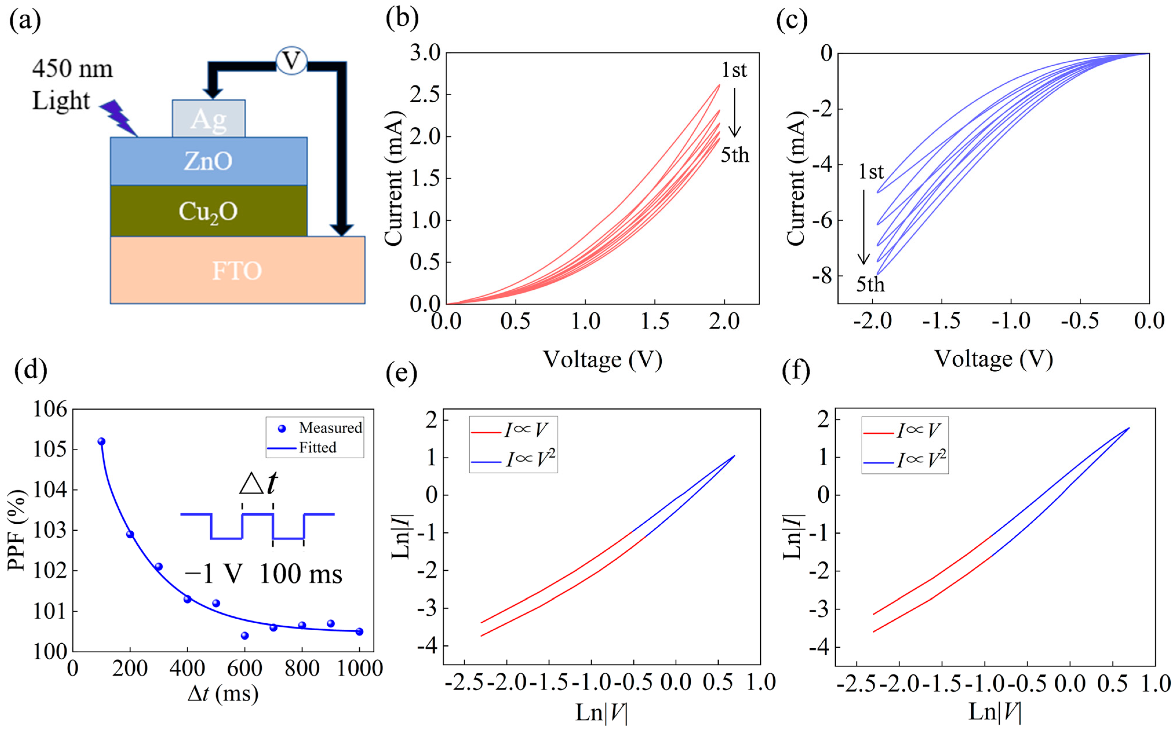
3.1. Electrical Performance Testing

Figure 1a shows the schematic structure of our designed optoelectronic memristor with Ag/ZnO/Cu2O/FTO. ZnO is a wide-bandgap semiconductor with excellent ultraviolet response properties, and its application in optoelectronic devices is mature [30]. Cu2O is a p-type semiconductor, often used in optoelectronic devices due to its high carrier mobility and high absorption coefficient in the visible region, as well as a direct bandgap structure and non-toxicity. We apply the voltage to the top electrode (Ag) for electrical measurement with 450 nm visible light above the device for optical measurement. Initially, the I-V curves for the memristive behavior of our devices were investigated. As demonstrated in Figure 1b,c, the device conductance showed a gradual increase or decrease in response to successive positive or negative voltage sweeps (0 V to 2 V and −2 V, respectively). This change in conductance is representative of analog resistive switching behavior and also indicates that the device has excellent synaptic plasticity. This sets the stage for further exploration of the synaptic nature of the device.
PPF synaptic behavior is simulated under the stimulation of two consecutive pulses. As expected, the current elicited by the second pulse (P2) is considerably larger than that triggered by the first pulse (P1). It is noteworthy that the PPF is determined by the time interval between the two consecutive pulses, as shown in Figure 1d. PPF is calculated as:
P P F = P 2 P 1 × 100 %
The relationship between PPF and pulse time interval can be fitted with a double exponential decay function. The formula is calculated as follows:
P P F = C 1 × e t τ 1 + C 2 × e t τ 2
Here t is the pulse time interval, C 1 and C 2 are the initial amplitudes, and τ 1 and τ 2 denote the characteristic relaxation times in synaptic behavior [31]. In biological synapses, the intensity of the second stimulus is influenced by the time interval between the two stimuli. The same phenomenon can be achieved in our device. The PPF index decreases gradually with increasing pulse intervals, τ 1 and τ 2 were fitted to 10.43 ms and 194.03 ms, respectively, indicating that our memristor can well simulate the PPF behavior of biological synapses.
To explore the working mechanism of the memristor device, the I-V curve is plotted on a logarithmic scale, as shown in Figure 1e,f. During the SET process, different voltage regions show different slopes. At lower voltages, there is a slope of 1 (I   V), suggesting an ohmic conduction process. At higher voltages, the slope increases to 2 (I   V2), and the current exhibits a voltage-squared dependence, following Child’s law, suggesting that the process is dominated by the trap-controlled space charge-limited conduction (SCLC) mechanism [32]. Furthermore, during the RESET process, the device also shows a similar process.
To further validate the synaptic plasticity, a series of pulses were applied to our device. As shown in Figure 2a, 50 voltage pulses were used to modulate the conductance. When 50 voltage pulses at −0.5 V were applied to the device, the conductance was gradually increased from 2.0 μs to 8.9 μs, which indicates the existence of an enhancement process. Conversely, when 50 voltage pulses at 0.5 V were applied to the device, the conductance reduced gradually. In summary, the conductance gradually increases in response to negative pulses, mimicking the enhancing behavior of biological synapses. In contrast, when a positive pulse is applied, the conductance decreases, similar to the inhibitory behavior in biological synapses. The device also exhibits stable and reproducible synaptic behavior during 500 pulses, as shown in Figure 2b. In addition, we performed a long-time durability test of the device, which exhibited a stable conductance for 600 s, as shown in Figure S1. This signifies that the memristor possesses excellent synaptic plasticity and working durability. We also calculated the nonlinearity (NL) of the device regarding the weight update, as shown in Figure S2. NL was calculated as follows:
N L = M ax G P ( n ) G D ( n ) for   n = 1   to   N
where GP(n) and GD(n) are the conductance values after the nth Potentiation-pulse and nth Depression-pulse, respectively. These conductance values are normalized and used to calculate NL, which is equal to 0 for a fully linear update process [33]. The NL of our device was calculated at 0.80.
Due to the synaptic plasticity of the device, we can take the next step of exploration based on LTP/LTD data. As shown in Figure 2c, a three-layer ANN was constructed using the CrossSim platform. The ANN can be used to recognize the images of handwritten digits, where the synaptic weights use values of conductance measured previously. Two datasets were used to train the ANN: large images of handwritten digits from the “Modified National Institute of Standards and Technology” dataset, and small images of handwritten digits. During the training process, the synaptic weights are updated according to the cumulative distribution functions of LTP/LTD processes. The training results of the two datasets are shown in Figure 2d,e. We can observe that the recognition accuracy is more than 80% after three epochs. The blue curve in the figure shows the ideal simulation result, where the recognition accuracy of the ideal artificial neural network exceeds 90% after five epochs, indicating that our memristor has a promising application in image recognition.

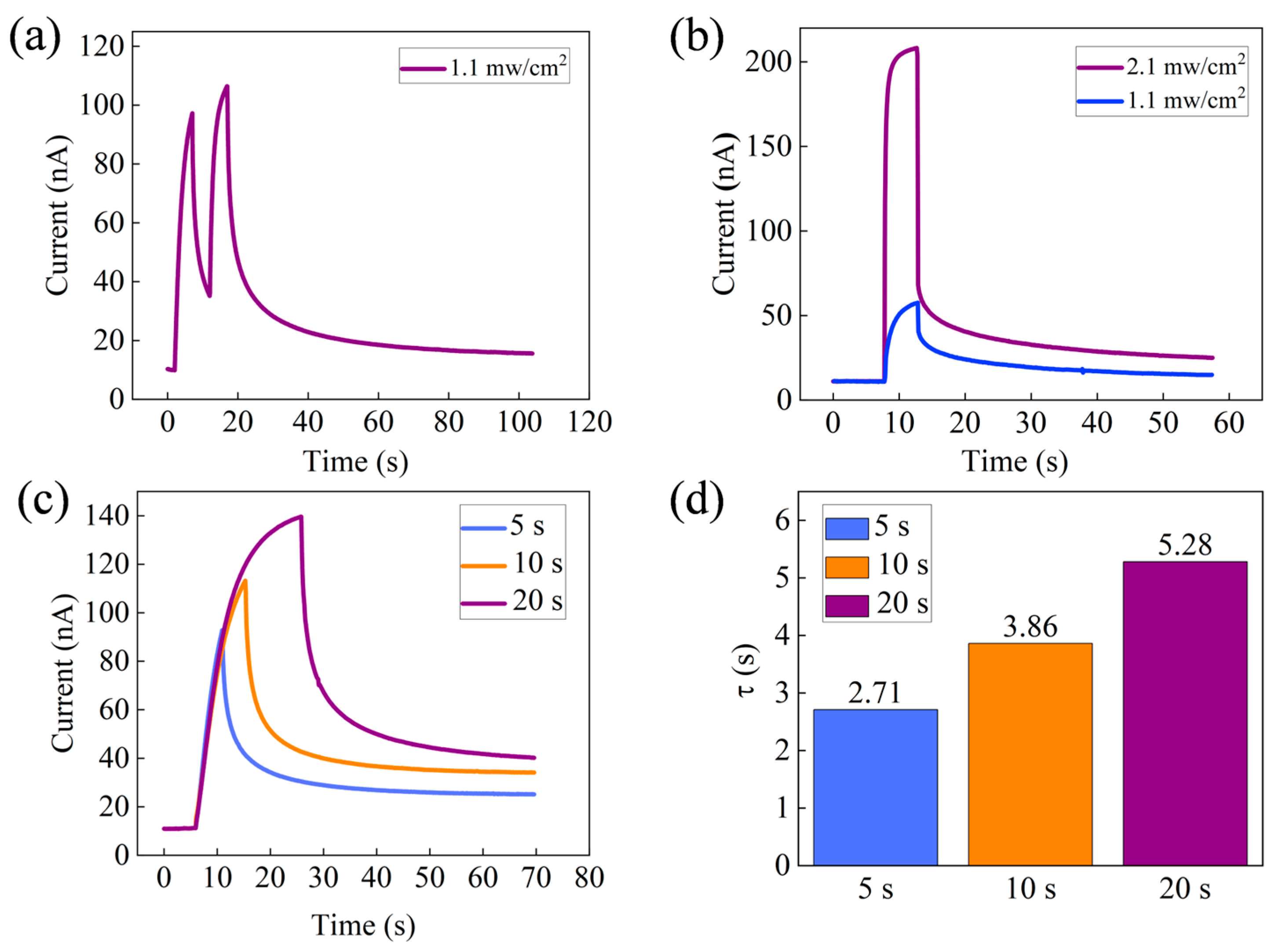
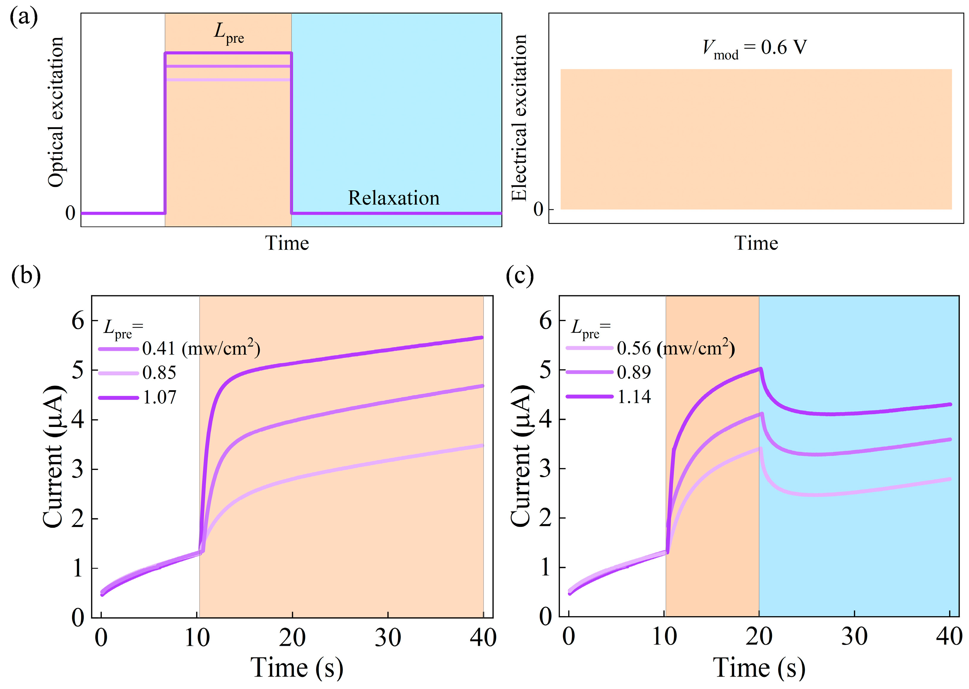
3.2. Optical Performance Testing

In the human visual system, visual synapses are responsible for converting optical information into electrical information, and similarly, artificial photoelectric synapses can be stimulated by light and respond electrically. Thus, the EPSC can be regarded as synaptic plasticity, which is important for characterizing the strength of synaptic stimuli [34]. In this study, light pulses of 5 s (1.1 mw/cm2) with a wavelength of 450 nm were used to induce EPSC. As shown in Figure 3a, the PPF of two light pulses with an interval of 5 s is 106.9%. In Figure 3b, increasing the intensity of light (2.1 mw/cm2) results in an increased amplitude of the EPSC. The spontaneous decay process following light irradiation is also governed by the light intensity. The higher the light intensity, the higher the value of the current that can remain after a specified duration of decay. Therefore, the transition from STP to LTP can be achieved by increasing the light intensity above the devices [35]. Our optoelectronic memristors can mimic synaptic behavior with low-energy consumption, and the average energy consumption per synaptic behavior is 10−9 J. In addition, we explored the photo response behavior of the optoelectronic memristor under visible light at 520 nm wavelength, as shown in Figure S3, the device achieved photo response under light pulses of 5 s, but the response intensity was not as high as under the 450 nm wavelength light stimulation, so 450 nm wavelength visible light was used for a series of experiments on photo response in this experiment.
Our device can also be used to simulate more complex synaptic functions by setting different light durations. Figure 3c demonstrates that when the light intensity is fixed, by varying different EPSC under different light durations (from 5 s to 20 s), the amplitude of the EPSC increases significantly with increasing light duration. It stands for the irradiation duration-dependent plasticity, which also marks the transition from STP to LTP. To evaluate the ability of synapses to retain memory after external stimulation, an exponential decay function is used to fit the current decay process over time t.
I ( t ) = I + ( I 0 I ) × e t t 0 τ
where I is the current, I0 is the EPSC by light pulses, I is the stabilized state decay current, and τ is the decay constant, which represents the relaxation time constant, for the forgetting rate. The decay behavior shown in the function is similar to the Ebbinghaus forgetting curve [36]. Assuming that human memory declines over time, the forgetting curves show how human brain information is lost over time [37]. The values of τ are fitted, and the fitting results are shown in Figure 3d. The values of τ vary with the duration of light, which are fitted to be 2.71, 3.86, and 5.28. It describes the τ values corresponding to different light durations, which increase with increasing light durations.
From a neurobiological perspective, the human cognitive system can gradually acquire knowledge through learning, and forgetting occurs naturally over time. When relearning the same knowledge, the cognitive system can relearn it with higher efficiency; the phenomenon is defined as experiential learning behavior [38]. In this study, a simulation of experiential learning behavior is successfully realized based on the Ag/ZnO/Cu2O/FTO optoelectronic memristor, as shown in Figure 3e,f. During the experiment, the device is first trained using light pulses, and its conductance value gradually increases with the number of pulses. After 50 light pulse stimulations, the device’s conductance increases from an initial 5.2 μs to 6.0 μs, this process simulates well the human brain’s first learning. After removing light pulses, the conductance decay initially shows an accelerated decay trend, which turns into a decelerated decay after a specific time node, and this nonlinear relaxation behavior corresponds to the LTP of biological synapses. After 130 s of natural relaxation, the conductance value decreases to the initial 5.2 μs, as shown in Figure S4, which shows the forgetting process of the human brain. Remarkably, when light pulses with the same parameters are applied for retraining, only 20 pulses are required to restore the conductance value to 6.0 μs, which has a remarkable biological similarity to the relearning behavior of the human brain.
Based on the complete electrical and optical synaptic behaviors, this study achieved the functional simulation of three-terminal synapses in a two-terminal device structure. Specifically, we design an adjustable synaptic, whose core function is to dynamically modulate the correlation characteristics between presynaptic and postsynaptic, to accomplish the precise modulation of the optical response mode and intensity of the device. In this work, the light signal (Lpre) and the electrical signal (Vmod) are used as the presynaptic stimulus and modulation signal inputs, respectively, while the photocurrent response is considered as the postsynaptic weight change, as shown in Figure 4a. We investigate the effect of optical stimulation on the synaptic response properties under constant voltage conditions. As shown in Figure 4b,c, Vmod is applied to the device, and the current is still rising slowly in the first 10 s without Lpre. When Lpre is applied to the memristor, the current of the device increases with the increase in light intensity and light duration, which indicates that the optoelectronic synapses still have excellent performance in the case where optoelectronic signals are jointly involved in modulating the synapses. When Lpre is removed, the forgetting process is effectively suppressed due to the existence of Vmod, i.e., the current first decreases and then slowly increases. The experimental results show that the application of Vmod will delay the rate of forgetting visual information, and Lpre can be used to deepen the strength of the visual system’s memory for information.

3.3. Mechanistic Explanation

Finally, the modulation mechanism of the optical response in our ZnO/Cu2O optoelectronic device is investigated, and the oxygen vacancies play an important role in the optical modulation [18]. Because ZnO (4.3 eV) has a higher electron affinity than Cu2O (3.2 eV) [39,40], the energy band structures of ZnO and Cu2O are shown in Figure 5a. They form an interfacial potential barrier region. When light is applied to the device, the oxygen vacancies on the ZnO and Cu2O ionize into oxygen ions and electrons (VO → VO2+ + 2e). The elevated oxygen ion concentration induces conduction band bending, which decreases the width of the interfacial barrier, thereby promoting the electrons to cross the barrier and ultimately enhancing the device current, as shown in Figure 5b. On the contrary, when light is removed, partially ionized oxygen ions (VO2+) recombine with oxygen vacancies, triggering spontaneous photocurrent decay, as shown in Figure 5c. Thus, light-induced ionization of oxygen vacancies and neutralization of oxygen vacancies upon removal of light are the main mechanisms used by our device to model optical synaptic behavior.

4. Discussion

In summary, we have designed and developed a heterojunction-based optoelectronic memristor. We have demonstrated that the device has great potential for constructing artificial synapses and is capable of realizing various synaptic functions, including LTP and LTD under electrical signal excitation. Furthermore, recognition of handwritten digits has been performed based on LTP/LTD parameters. In addition, the optical properties of the device are further investigated by adjusting the light signal parameters, and synaptic behaviors such as STP, LTP, and learning-forgetting-relearning are simulated. Moreover, based on the combined modulation of optical and electrical signals of the device, the visual synaptic function is achieved. In this visual synaptic, the memory strength and forgetting rate can be changed by adjusting the optoelectronic signals. Since the device generates optical responses at both 450 nm and 520 nm wavelengths, the potential and applications of the device for multi-wavelength sensing can be explored in the future to realize more complex optoelectronic synaptic functions. The optoelectronic synaptic device proposed in this work provides a hardware foundation for the next-generation artificial vision system and explores the possibility of designing neuromorphic devices in the future.

Supplementary Materials

The following supporting information can be downloaded at: https://www.mdpi.com/article/10.3390/electronics14122490/s1. Figure S1. Long time stability test of the device. Figure S2. Normalized conductance of 50 pulses. Figure S3. Synaptic behavior under light stimulation of 520 nm wavelength. Figure S4. Forget behaviors. Table S1. compared the present work with some previous optoelectronic memristors.

Author Contributions

Conceptualization, C.M.; methodology, C.M. and H.L.; validation, C.M. and H.L.; data curation, C.M. and T.L.; writing—original draft preparation, C.M.; writing—review and editing, S.Z. and T.L.; visualization, C.M. and J.L.; supervision, S.Z. and H.L.; project administration, S.Z.; funding acquisition, S.Z. All authors have read and agreed to the published version of the manuscript.

Funding

This research is supported by the National Natural Science Foundation of China (61871451), Guizhou Province Science and Technology Plan Project No. ZK [2024]. Key Project 078, the Joint Fund of Bijie City and Guizhou University of Engineering Science (Bijie Science and Technology Union Contract [2023]. No. 16).

Data Availability Statement

The raw data supporting the conclusions of this article will be made available by the authors on request.

Acknowledgments

We thank Martin Dove for the contribution to this paper in terms of writing improvement.

Conflicts of Interest

The authors declare no conflicts of interest.

References

  1. Li, G.; Xie, D.; Zhong, H.; Zhang, Z.; Fu, X.; Zhou, Q.; Li, Q.; Ni, H.; Wang, J.; Guo, E.J.; et al. Photo-induced non-volatile VO(2) phase transition for neuromorphic ultraviolet sensors. Nat. Commun. 2022, 13, 1729. [Google Scholar] [CrossRef] [PubMed]
  2. Zhang, L.; Yu, H.; Xiao, C.; Si, J.; Xu, H.; Zhu, W.; Wang, L. Building Light Stimulated Synaptic Memory Devices for Visual Memory Simulation. Adv. Electron. Mater. 2021, 7, 2000945. [Google Scholar] [CrossRef]
  3. Lee, H.R.; Lee, D.; Oh, J.H. A Hippocampus-Inspired Dual-Gated Organic Artificial Synapse for Simultaneous Sensing of a Neurotransmitter and Light. Adv. Mater. 2021, 33, 2100119. [Google Scholar] [CrossRef]
  4. Li, Y.; Wang, J.H.; Yang, Q.; Shen, G.Z. Flexible Artificial Optoelectronic Synapse based on Lead-Free Metal Halide Nanocrystals for Neuromorphic Computing and Color Recognition. Adv. Sci. 2022, 9, 2202123. [Google Scholar] [CrossRef]
  5. Yang, X.; Xiong, Z.; Chen, Y.; Ren, Y.; Zhou, L.; Li, H.; Zhou, Y.; Pan, F.; Han, S.T. A self-powered artificial retina perception system for image preprocessing based on photovoltaic devices and memristive arrays. Nano Energy 2020, 78, 105246. [Google Scholar] [CrossRef]
  6. Sun, F.; Lu, Q.; Feng, S.; Zhang, T. Flexible Artificial Sensory Systems Based on Neuromorphic Devices. ACS Nano 2021, 15, 3875–3899. [Google Scholar] [CrossRef] [PubMed]
  7. Jaafar, A.H.; Kemp, N.T. Light-Mediated Multilevel Neuromorphic Switching in a Hybrid Organic–Inorganic Memristor. ACS Omega 2024, 9, 51641–51651. [Google Scholar] [CrossRef] [PubMed]
  8. Strukov, D.B.; Snider, G.S.; Stewart, D.R.; Williams, R.S. The missing memristor found. Nature 2008, 453, 80–83. [Google Scholar] [CrossRef]
  9. Jo, S.H.; Chang, T.; Ebong, I.; Bhadviya, B.B.; Mazumder, P.; Lu, W. Nanoscale Memristor Device as Synapse in Neuromorphic Systems. Nano Lett. 2010, 10, 1297–1301. [Google Scholar] [CrossRef]
  10. Mao, J.-Y.; Zhou, L.; Zhu, X.; Zhou, Y.; Han, S.-T. Photonic Memristor for Future Computing: A Perspective. Adv. Opt. Mater. 2019, 7, 1900766. [Google Scholar] [CrossRef]
  11. Shan, X.; Zhao, C.; Wang, X.; Wang, Z.; Fu, S.; Lin, Y.; Zeng, T.; Zhao, X.; Xu, H.; Zhang, X.; et al. Plasmonic Optoelectronic Memristor Enabling Fully Light-Modulated Synaptic Plasticity for Neuromorphic Vision. Adv. Sci. 2022, 9, 2104632. [Google Scholar] [CrossRef] [PubMed]
  12. Yue, L.; Sun, H.; Zhu, Y.; Li, Y.; Yang, F.; Dong, X.; Chen, J.; Zhang, X.; Chen, J.; Zhao, Y.; et al. Electrical-Light Coordinately Modulated Synaptic Memristor Based on Ti3C2 MXene for Near-Infrared Artificial Vision Applications. J. Phys. Chem. Lett. 2024, 15, 8667–8675. [Google Scholar] [CrossRef]
  13. Wen, Y.; Cao, Y.; Ren, H.; Du, X.; Guo, J.; Wu, Z.; Liu, W.; Du, J.; Zhang, Y. Ferroelectric Optical Memristors Enabled by Non-Volatile Electro-Optic Effect. Adv. Mater. 2025, 37, 2417658. [Google Scholar] [CrossRef]
  14. Hu, L.; Yang, J.; Wang, J.; Cheng, P.; Chua, L.O.; Zhuge, F. All-Optically Controlled Memristor for Optoelectronic Neuromorphic Computing. Adv. Funct. Mater. 2021, 31, 2005582. [Google Scholar] [CrossRef]
  15. Kumar, D.; Bharti, R.; Li, H.; Kumbhar, D.D.; El-Atab, N. Optoelectronic wide-band-gap oxide-based memristor for mimicking human eye sensory perception and object tracking. Cell Rep. Phys. Sci. 2024, 5, 102144. [Google Scholar] [CrossRef]
  16. Wang, X.; Chen, F.; Li, X.; Xiang, T.; Wang, L. Emulation of Optoelectronic Synaptic Behavior in a MoS2/WSe2-Based p–n van der Waals Heterostructure Memtransistor. ACS Appl. Electron. Mater. 2024, 6, 4311–4320. [Google Scholar] [CrossRef]
  17. Kim, H.; Lee, K.; Zan, G.; Shin, E.; Kim, W.; Zhao, K.; Jang, G.; Moon, J.; Park, C. Chiroptical Synaptic Perovskite Memristor as Reconfigurable Physical Unclonable Functions. ACS Nano 2025, 19, 691–703. [Google Scholar] [CrossRef]
  18. Li, X.; Fang, Z.; Guo, X.; Wang, R.; Zhao, Y.; Zhu, W.; Wang, L.; Zhang, L. Light-Induced Conductance Potentiation and Depression in an All-Optically Controlled Memristor. ACS Appl. Mater. Interfaces 2024, 16, 27866–27874. [Google Scholar] [CrossRef]
  19. Zheng, J.; Du, Y.; Dong, Y.; Shan, X.; Tao, Y.; Lin, Y.; Zhao, X.; Wang, Z.; Xu, H.; Liu, Y. Fully light-modulated memristor based on ZnO/MoOx heterojunction for neuromorphic computing. Appl. Phys. Lett. 2024, 124, 133502. [Google Scholar] [CrossRef]
  20. Zhou, Z.; Pei, Y.; Zhao, J.; Fu, G.; Yan, X. Visible light responsive optoelectronic memristor device based on CeOx/ZnO structure for artificial vision system. Appl. Phys. Lett. 2021, 118, 191103. [Google Scholar] [CrossRef]
  21. Yin, S.; Song, C.; Sun, Y.; Qiao, L.; Wang, B.; Sun, Y.; Liu, K.; Pan, F.; Zhang, X. Electric and Light Dual-Gate Tunable MoS2 Memtransistor. ACS Appl. Mater. Interfaces 2019, 11, 43344–43350. [Google Scholar] [CrossRef] [PubMed]
  22. Li, R.; Wang, W.; Li, Y.; Gao, S.; Yue, W.; Shen, G. Multi-modulated optoelectronic memristor based on Ga2O3/MoS2 heterojunction for bionic synapses and artificial visual system. Nano Energy 2023, 111, 108398. [Google Scholar] [CrossRef]
  23. Cheng, Y.K.; Li, Z.Z.; Lin, Y.; Wang, Z.Q.; Shan, X.Y.; Tao, Y.; Zhao, X.N.; Xu, H.Y.; Liu, Y.C. Color Recognition Achieved in Multiwavelength Controlled Plasmonic Optoelectronic Memristor for Neuromorphic Visual System. Adv. Funct. Mater. 2024, 35, 2414404. [Google Scholar] [CrossRef]
  24. Shrivastava, S.; Dai, W.S.; Limantoro, S.E.; Juliano, H.; Tseng, T.Y. A Violet-Light-Responsive ReRAM Based on Zn2SnO4/Ga2O3 Heterojunction as an Artificial Synapse for Visual Sensory and In-Memory Computing. Adv. Electron. Mater. 2024, 11, 2400527. [Google Scholar] [CrossRef]
  25. Shan, X.; Zhao, C.; Lin, Y.; Liu, J.; Zhang, X.; Tao, Y.; Wang, C.; Zhao, X.; Wang, Z.; Xu, H.; et al. Optoelectronic synaptic device based on ZnO/HfOx heterojunction for high-performance neuromorphic vision system. Appl. Phys. Lett. 2022, 121, 263501. [Google Scholar] [CrossRef]
  26. Li, Z.; Zou, G.; Xiao, Y.; Feng, B.; Huo, J.; Peng, J.; Sun, T.; Liu, L. MoS2/ZnO-heterostructured optoelectronic synapse for multiwavelength optical information-based sensing, memory, and processing. Nano Energy 2024, 127, 109733. [Google Scholar] [CrossRef]
  27. Yang, J.; Hu, L.; Shen, L.; Wang, J.; Cheng, P.; Lu, H.; Zhuge, F.; Ye, Z. Optically driven intelligent computing with ZnO memristor. Fundam. Res. 2024, 4, 158–166. [Google Scholar] [CrossRef]
  28. Yin, S.; Jiang, Z.; Kim, M.; Gupta, T.; Seok, M.; Seo, J.S. Vesti: Energy-Efficient In-Memory Computing Accelerator for Deep Neural Networks. IEEE Trans. Very Large Scale Integr. (VLSI) Syst. 2020, 28, 48–61. [Google Scholar] [CrossRef]
  29. Antolini, A.; Lico, A.; Zavalloni, F.; Scarselli, E.F.; Gnudi, A.; Torres, M.L.; Canegallo, R.; Pasotti, M. A Readout Scheme for PCM-Based Analog In-Memory Computing With Drift Compensation Through Reference Conductance Tracking. IEEE Open J. Solid-State Circuits Soc. 2024, 4, 69–82. [Google Scholar] [CrossRef]
  30. Khan, R.; Raziq, F.; Ahmad, I.; Ghosh, S.; Kheawhom, S.; Sangaraju, S. Reliable Resistive Switching and Multifunctional Synaptic Behavior in ZnO/NiO Nanocomposite Based Memristors for Neuromorphic Computing. Acs. Appl. Electron. Mater. 2024, 7, 73–85. [Google Scholar] [CrossRef]
  31. Han, C.; Han, X.; Han, J.; He, M.; Peng, S.; Zhang, C.; Liu, X.; Gou, J.; Wang, J. Light-Stimulated Synaptic Transistor with High PPF Feature for Artificial Visual Perception System Application. Adv. Funct. Mater. 2022, 32, 2113053. [Google Scholar] [CrossRef]
  32. Teja Nibhanupudi, S.S.; Roy, A.; Veksler, D.; Coupin, M.; Matthews, K.C.; Disiena, M.; Singh, J.V.; Gearba-Dolocan, I.R.; Warner, J.; Kulkarni, J.P.; et al. Ultra-fast switching memristors based on two-dimensional materials. Nat. Commun. 2024, 15, 2334. [Google Scholar] [CrossRef]
  33. Wang, I.T.; Chang, C.-C.; Chiu, L.-W.; Chou, T.; Hou, T.-H. 3D Ta/TaOx/TiO2/Ti synaptic array and linearity tuning of weight update for hardware neural network applications. Nanotechnology 2016, 27, 365204. [Google Scholar] [CrossRef]
  34. Hao, D.; Yang, Z.; Huang, J.; Shan, F. Recent Developments of Optoelectronic Synaptic Devices Based on Metal Halide Perovskites. Adv. Funct. Mater. 2023, 33, 2211467. [Google Scholar] [CrossRef]
  35. Zhong, Y.; Yin, J.; Li, M.; He, Y.; Lei, P.; Zhong, L.; Liao, K.; Wu, H.; Wang, Z.; Jie, W. High-performance memristor for energy-efficient artificial optoelectronic synapse based on BiVO4 nanosheets. J. Alloys Compd. 2024, 991, 174533. [Google Scholar] [CrossRef]
  36. Chen, X.; Chen, B.; Jiang, B.; Gao, T.; Shang, G.; Han, S.-T.; Kuo, C.-C.; Roy, V.A.L.; Zhou, Y. Nanowires for UV–vis–IR Optoelectronic Synaptic Devices. Adv. Funct. Mater. 2023, 33, 2208807. [Google Scholar] [CrossRef]
  37. Li, Y.; Sun, H.; Yue, L.; Yang, F.; Dong, X.; Chen, J.; Zhang, X.; Chen, J.; Zhao, Y.; Chen, K.; et al. Multicolor Fully Light-Modulated Artificial Synapse Based on P-MoSe2/PxOy Heterostructured Memristor. J. Phys. Chem. Lett. 2024, 15, 8752–8758. [Google Scholar] [CrossRef]
  38. Yang, W.; Kan, H.; Shen, G.; Li, Y.A. Network Intrusion Detection System with Broadband WO3–x/WO3–x-Ag/WO3–x Optoelectronic Memristor. Adv. Funct. Mater. 2024, 34, 2312885. [Google Scholar] [CrossRef]
  39. Jabeen, S.; Ismail, M.; Rana, A.M.; Ahmed, E. Impact of work function on the resistive switching characteristics of M/ZnO/CeO2/Pt devices. Mater. Res. Express 2017, 4, 056401. [Google Scholar] [CrossRef]
  40. Murali, D.S.; Aryasomayajula, S. Thermal conversion of Cu4O3 into CuO and Cu2O and the electrical properties of magnetron sputtered Cu4O3 thin films. Appl. Phys. A 2018, 124, 279. [Google Scholar] [CrossRef]
Figure 1. Synaptic behaviors under electrical signals. (a) Schematic diagram of the device. (b) The I-V curve of the device under 5 consecutive forward and (c) negative voltage sweeps. (d) Variation in PPF index with pulse interval. (e) Forward and (f) Negative voltage profile in logarithmic scale coordinates.
Electronics 14 02490 g001
Figure 2. (a) Conductance modulation through the use of 50 voltage pulses (−0.5 V for conductance enhancement, 0.5 V for conductance suppression). (b) 5-cycle process of the device modulated by 100 voltage pulses. (c) Schematic of neural network for recognizing 28 × 28 pixel handwritten digital images. Training results for (d) 8 × 8 and (e) 28 × 28 pixel handwritten digital images.
Electronics 14 02490 g002
Figure 3. Synaptic behavior under light stimulation (Reading voltage = 0.01 V) (a) EPSC induced by two light pulses. (b) EPSC induced by different light intensities. (c) EPSC induced by different light durations at a fixed light intensity. (d) Statistics of synaptic relaxation time after different light durations. (e) First learning behavior. (f) Relearning behavior.
Electronics 14 02490 g003aElectronics 14 02490 g003b
Figure 4. Synaptic behavior under co-modulation of optoelectronic signals (a) Pulse waveforms of optical excitation and electrical excitation. (b) Changes in photocurrent caused by changes in Lpre. (c) Modulation of synapses by Vmod after withdrawal of Lpre. The brown part represents the light state, and the blue part represents the state after removing the light.
Electronics 14 02490 g004
Figure 5. Schematic diagram of energy band changes in the (a) dark state, (b) light illumination state, and (c) removal light state. The green part represents ZnO and the brown part represents Cu2O. The dash lines represent the bending and recovery of the energy bands.
Electronics 14 02490 g005
Disclaimer/Publisher’s Note: The statements, opinions and data contained in all publications are solely those of the individual author(s) and contributor(s) and not of MDPI and/or the editor(s). MDPI and/or the editor(s) disclaim responsibility for any injury to people or property resulting from any ideas, methods, instructions or products referred to in the content.

