1. Introduction
Neural networks have transformed computational systems by efficiently addressing a wide variety of complex challenges. Their extensive applications include image processing, natural language understanding, and real-time decision making. Among neural networks, Convolutional Neural Networks (CNNs) have particularly excelled in tasks such as image recognition and classification, making them crucial for processing visual data [
1]. However, deploying CNNs on resource-constrained edge devices, like smartphones, IoT sensors, and wearable gadgets, presents significant challenges. These devices typically have limited power, storage, and processing capabilities. Therefore, developing methods that efficiently bridge high-performance neural network requirements with the constraints inherent to edge computing environments is an active and critical research area [
2]. A prominent method for improving CNN efficiency is the Winograd algorithm, which optimizes the convolution process by significantly reducing multiplications, the primary computational operation in CNNs. Though this reduces computational overhead and enhances processing speed and energy efficiency, it increases the number of required additions [
3]. Additionally, enabling on-device learning is vital for real-time adaptability and privacy in applications that demand responsiveness and customization, further emphasizing the need for optimized computational resources and specialized memory structures [
4,
5].
Efficient deployment of the Winograd algorithm and on-device learning [
6,
7,
8] requires specialized memory architectures, such as transposable memories, which efficiently handle the specific data access patterns of CNN operations [
9,
10,
11,
12]. Traditional memory technologies, such as Static Random Access Memory (SRAM), consume significant chip area and exhibit high leakage power even in idle states, making them unsuitable for edge applications with stringent energy and area constraints. Addressing these challenges is essential to unlocking CNNs’ full potential on edge devices [
13,
14].
To address the drawbacks of traditional memories, recent studies have explored Non-Volatile Memory (NVM) technologies, such as Magnetoresistive Random Access Memory (MRAM), due to their minimal static power consumption and non-volatility. Magnetic Tunnel Junctions (MTJs), key components in MRAM technology, have been utilized in transposable memory designs. Previous approaches primarily employed Spin-Transfer Torque (STT) to write data into transposable memory arrays. Although effective, STT-based methods face limitations in terms of slow write operations and higher energy consumption, making them less suitable for energy-sensitive applications. Alternative approaches leveraging Spin Hall Effect (SHE)-assisted STT improve write efficiency but often require multiple cycles to perform transposed data reads, reducing overall performance in scenarios demanding high-speed access [
15]. Furthermore, certain prior works [
16,
17] introduced diagonal data storage combined with shifting and switching circuitry to facilitate transposed access, while these designs improve some aspects, they tend to be inefficient for handling smaller bit-width data, such as binary or quaternary, and exhibit complexity issues with multi-bit data. Such limitations highlight the necessity for more adaptable and efficient transposable memory solutions.
In this paper, we propose a novel transposed MRAM (T-MRAM) architecture using Magnetic Tunnel Junctions (MTJs) with SHE-assisted STT for efficient data writing. Our approach enables simultaneous writing to four MTJs using a single SHE current, significantly reducing power consumption and enhancing energy efficiency. Furthermore, the design incorporates stacked MTJs to increase data storage density. The proposed memory architecture effectively supports both normal and transposed data accesses, regardless of bit-width, making it versatile and well-suited for diverse CNN applications. Extensive simulations demonstrate that our proposed architecture achieves substantial improvements in energy efficiency, power consumption, and processing speed, making it a highly effective solution for CNN accelerators deployed in resource-constrained edge environments.
3. Proposed WinEdge Architecture
3.1. T-MRAM Cell
As illustrated in
Figure 3a, our proposed T-MRAM cell employs a SHE-assisted STT mechanism for efficient data writing and storage operations. To significantly reduce power consumption, the SHE current simultaneously targets two memory cells comprising four MTJs. During the write operation, the SHE current passes through transistor TW-1 by activating the word line WLW. Concurrently, the source lines (SL) SL-1 and SL-2 are set to V
DD and ground, respectively. Following the application of the SHE current, the magnetization vectors of the MTJs align perpendicular to the initial orientation, thus achieving a transient intermediate magnetization state. Subsequently, the STT current path is activated once this intermediate state is reached. Intermediate voltage levels are then applied to the SLs, while bit lines (BL1 and BL2) are driven to either ground or V
DD depending on the desired data state, completing the magnetic orientation switch.
In the two stacked MTJs, a data-dependent path is established between either 0 V and the intermediate voltage or V
DD and the intermediate voltage, and the appropriate state is written to the cells.
Figure 3a illustrates the detailed interconnections and simultaneous write operations of the proposed T-MRAM cells.
Table 1 summarizes the logic states and corresponding interconnect values utilized during the simultaneous 4-bit data (‘1001’) writing operation, facilitated by the activation of transistors T1, T2, and T3. This approach achieves efficient data writing within a single clock cycle. Furthermore, the physical layout of the proposed T-MRAM cell designed based on the
-based scaling rule, is depicted in
Figure 3b. Note that in each of the two sections labeled as MTJs in this figure, two MTJ cells are designed in a stacked configuration.
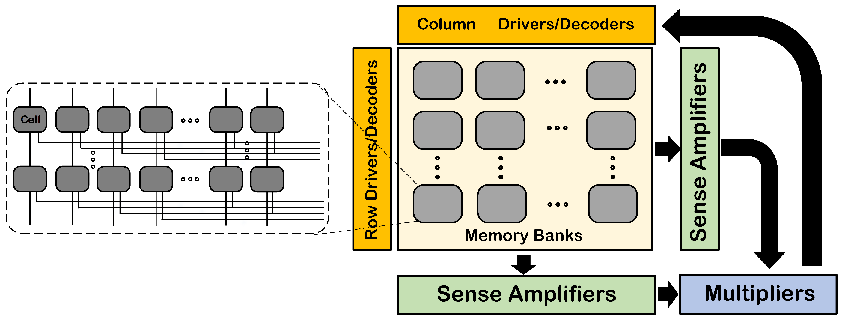
3.2. Proposed Memory Array
Figure 4 illustrates the detailed architecture of the proposed transposed memory array, designed explicitly for efficient data storage and retrieval in neural network acceleration applications. The memory array is partitioned into multiple memory banks, each capable of independently accessing stored data in both normal and transposed orientations. This dual-mode access significantly enhances computational flexibility, allowing seamless integration with convolution algorithms such as the Winograd algorithm. In this design, dedicated vertical and horizontal sense amplifiers (SAs) enable rapid and efficient data retrieval from the memory cells. The retrieved data are directly transferred to the integrated computational unit, facilitating high-speed data processing critical for edge device operations. Computation outcomes are subsequently written back into the memory via specialized address lines, ensuring data integrity and consistency throughout processing cycles.
Figure 4 further details the internal connectivity structure of the memory cells within each bank, illustrating how each cell comprises two stacked MTJs. This configuration permits versatile storage capacities, supporting various bit-width requirements and data precision levels ranging from binary to multi-bit formats. The design achieves optimized performance by allowing simultaneous access to multiple bits, thereby reducing overall latency and enhancing throughput for diverse data-intensive applications.
Figure 5 illustrates the detailed storage and data access schemes for various bit-width configurations, specifically highlighting binary, quaternary, and four-bit data arrangements. This figure demonstrates the proposed memory array’s capability for efficient simultaneous access in both normal (row-wise) and transposed (column-wise) directions. In
Figure 5a, the storage configuration for binary data is depicted, where each MTJ stores a single bit. Normal data access is performed by grounding the source lines, and using the BL2 bit lines connected to sense amplifiers (SAs), enabling rapid retrieval of stored data. For transposed data access, the architecture uses dedicated transposed bit lines (BLT) connected to SAs, while the BL1 bit lines are grounded, ensuring equally efficient data retrieval in column-wise orientation.
Figure 5b demonstrates the quaternary data storage and access scheme, where each cell stores two bits of data across two stacked MTJs. Here, normal data retrieval involves connecting BL2 lines to the SAs and grounding BL1 lines, allowing simultaneous access to both bits stored in a single cell. Conversely, transposed access utilizes BLT lines connected to SAs and grounded BL1 lines, enabling efficient and parallel retrieval of column-wise stored data.
In the four-bit data arrangement illustrated in
Figure 5c, each data element spans two adjacent memory cells, thereby accommodating four bits of storage per matrix element. For normal mode retrieval, each data element is accessed through two consecutive SAs, with BL2 lines connecting directly to the SAs and BL1 lines grounded. For transposed access, BLT lines (BLT1 and BLT2) are sequentially connected to consecutive SAs to read individual bits efficiently. This systematic approach ensures flexible, high-speed data handling in both normal and transposed memory orientations, making the proposed architecture highly suitable for resource-constrained neural network acceleration tasks.
Figure 6 presents a comprehensive timing diagram demonstrating the operational performance of a representative segment of the proposed memory array, specifically focusing on the data access methods depicted in
Figure 5b. During the initial 5 nanoseconds, binary data are written sequentially to the first row, comprising four MTJ cells. In the subsequent interval of 5 nanoseconds, the write operation is replicated for the second row. This controlled sequential writing process ensures accurate initialization of data prior to read operations. Following these write phases, the memory array undergoes standard read operations. The first row is accessed during the 15–20 ns window, where data integrity and state verification are performed through the connected SAs. Similarly, the second row undergoes a normal read operation between 20 and 25 ns, allowing confirmation of the successful data storage and retrieval for each MTJ cell.
To validate transposed access capabilities, two separate intervals are allocated specifically for reading data stored column-wise. The first transposed read operation occurs between 30 and 35 ns, targeting the first column. Subsequently, the second column data are read from 35 to 40 ns. This sequential column-wise access highlights the flexibility of the proposed architecture, demonstrating its effectiveness in rapidly switching between normal and transposed data retrieval modes. This detailed operational timeline, visually represented in
Figure 6, underscores the high efficiency, reliability, and versatility of our T-MRAM array architecture. It confirms the design’s ability to achieve rapid simultaneous data writing and flexible, efficient reading operations, both critical for high-performance neural network acceleration in resource-constrained edge computing environments. Leveraging the dual-mode access capabilities of our T-MRAM array, we now present its strategic mapping for neural network computation, specifically optimized for the Winograd convolution algorithm.
3.3. Hardware Mapping
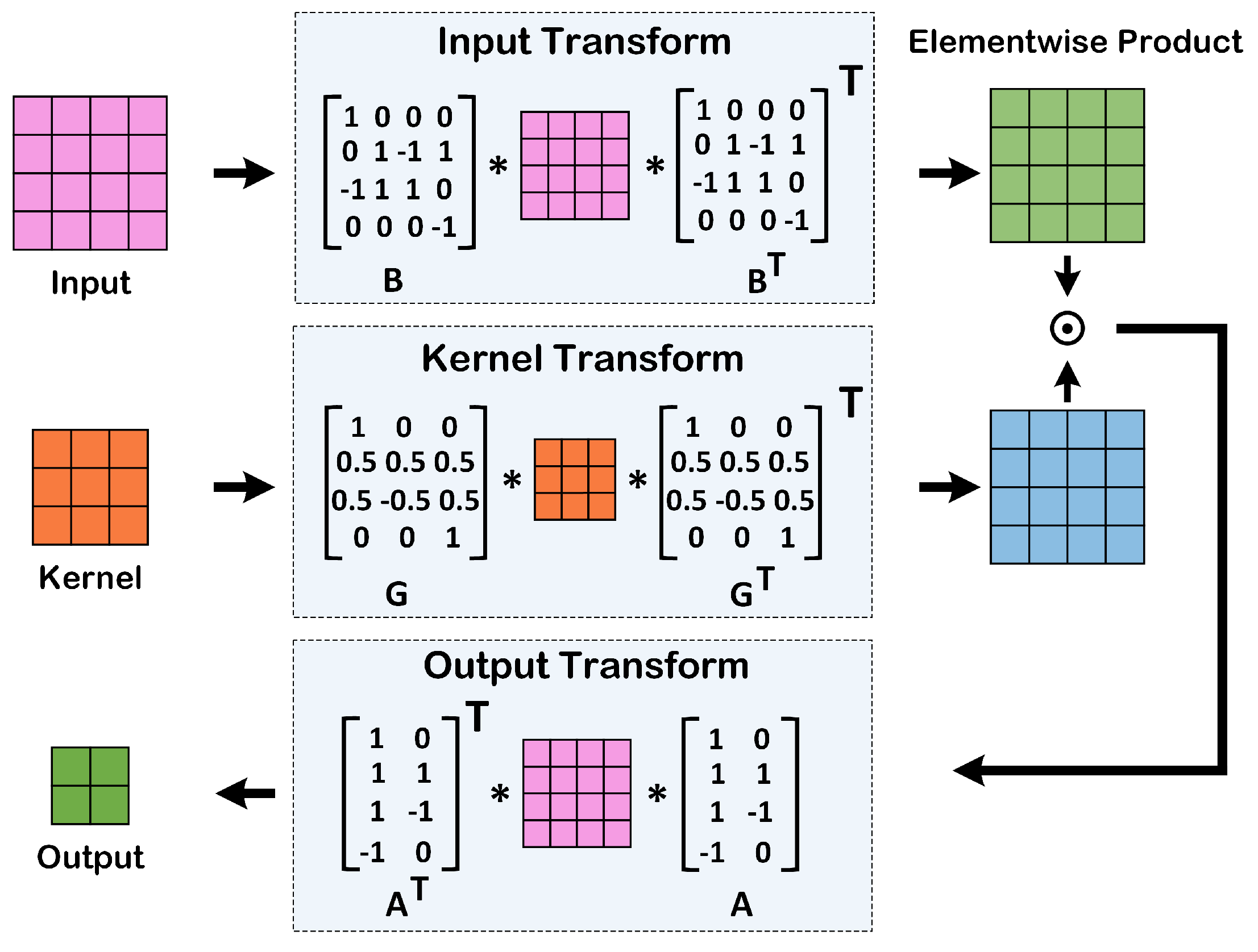
The proposed T-MRAM architecture is strategically designed to facilitate efficient mapping of convolutional neural networks, particularly employing the Winograd algorithm. Initially, convolution kernels and input feature maps are partitioned into sub-matrices that align with the T-MRAM’s storage structure. Each sub-matrix element is then stored within individual MTJs, allowing efficient simultaneous access during both normal and transposed data reads. Specifically, the convolution operation, performed using the Winograd algorithm, benefits from the transposable memory capability. During the transformation phase, input data and kernels undergo transformation utilizing matrices and . The resultant transformed data and kernels are stored in normal access mode. For subsequent matrix multiplications and element-wise operations (Hadamard product), the architecture seamlessly switches to transposed access mode. The sense amplifiers retrieve rows and columns simultaneously, feeding data directly into the computational sub-arrays for efficient execution of arithmetic operations.
Following the element-wise multiplication, the results undergo an inverse transformation using matrix , converting back to the spatial domain. These final output matrices are subsequently written back into the memory cells. This approach optimally utilizes the transposed memory structure, significantly minimizing data movement, latency, and overall power consumption. Such streamlined hardware mapping underscores the suitability of the proposed T-MRAM architecture for resource-constrained CNN acceleration in edge computing environments.
4. Experiments
Circuit-level simulations were performed using HSPICE with the 45 nm NCSU Product Development Kit (PDK) library [
21] and a validated MTJ compact model [
22] at a nominal supply voltage of 1.2 V.
Table 2 summarizes the critical MTJ parameters used in the simulations, ensuring accurate modeling of physical characteristics and performance metrics of the proposed T-MRAM cell.
To enhance reproducibility, we provide key simulation parameters used in our evaluations, summarized in
Table 3. The proposed T-MRAM array supports binary, quaternary, and 4-bit data formats via a stacked MTJ structure and dual-mode access architecture. A nominal activity factor of 0.5 was used to model alternating read/write behavior. For algorithm-level testing, we implemented a
input with a
kernel using the Winograd
configuration. Representative layers from ShuffleNet, ResNet18, TinyYOLO, MobileNetV2, and EfficientNet-V0 were selected as workloads. All simulations were performed in HSPICE using the 45 nm NCSU FreePDK at 1.2 V and 25 °C. Each memory access was modeled over a 5 ns window.
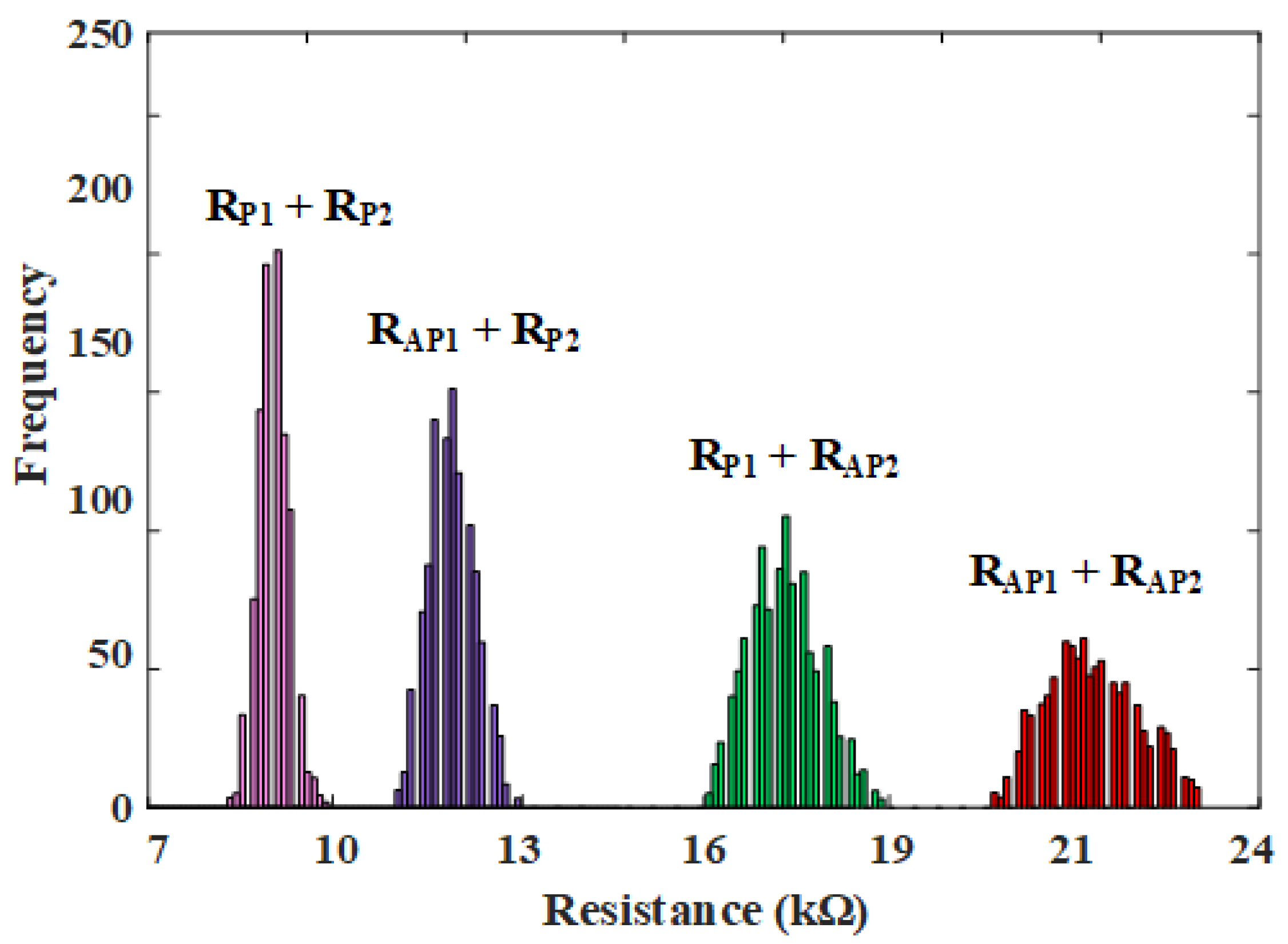
To evaluate robustness and reliability against process variations, extensive Monte Carlo simulations comprising 1000 iterations were executed. Specifically, variations in critical fabrication parameters, including free layer thickness (T
F), free layer surface area, MTJ resistance-area product, and Tunneling Magnetoresistance (TMR) were modeled using Gaussian distributions with standard deviations of 5%, 15%, 15%, and 10%, respectively [
23,
24]. Reliable multi-bit storage requires distinct resistance states despite fabrication inconsistencies;
Figure 7 demonstrates the clearly distinguishable four resistance states achieved under these process variations, confirming the robustness of the proposed design.
To validate the performance and efficiency of the proposed T-MRAM architecture for convolution acceleration, the Winograd algorithm was implemented for a standard convolution scenario involving a
input matrix and a
kernel. Comparative assessments against existing designs [
17] were conducted, evaluating key performance metrics, including processing delay, power consumption, and Power-Delay Product (PDP). As summarized in
Table 4, the proposed architecture achieves a power consumption of 136
W, a processing delay of 807 ns, and a PDP of 110 pJ. These results demonstrate substantial improvements over existing approaches, showcasing reductions of approximately 33% in power consumption and up to 72% in PDP relative to comparable spintronic-based implementations. Additionally, static power analysis emphasizes the considerable energy advantages, with near-zero static power consumption compared to conventional SRAM-based solutions, which exhibit significantly higher leakage power.
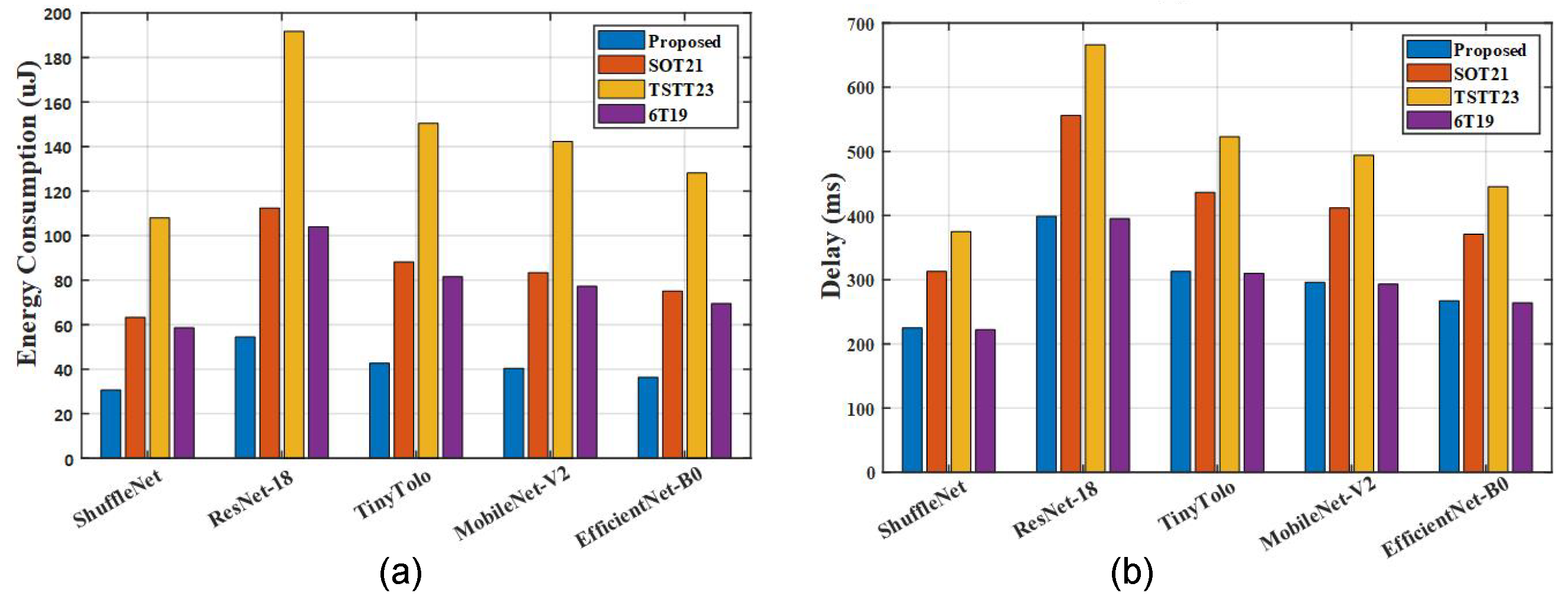
For a comprehensive performance evaluation, practical neural network workloads were considered.
Figure 8 presents performance comparisons across several widely used CNN architectures, including ShuffleNet, ResNet18, TinyYOLO, MobileNetV2, and EfficientNet-V0. These comparisons underscore substantial reductions in power and energy consumption—achieving at least 36% power and 47% energy savings compared to existing designs. These improvements are primarily attributable to our optimized design features, such as simultaneous multi-bit reading and writing capabilities, which significantly reduce memory access overhead and enhance computational throughput. Furthermore, the proposed architecture’s execution latency closely matches the state-of-the-art optimized approach described in [
17], demonstrating approximately a 28% improvement compared to other evaluated designs. These results collectively confirm the viability and superior performance of our T-MRAM architecture for resource-efficient CNN acceleration in edge computing environments.
5. Discussion and Conclusions
In this paper, we introduced a novel T-MRAM architecture, namely WinEdge, that significantly advances Winograd convolution acceleration for edge computing. Our design combines SHE-assisted STT writing with stacked MTJs to achieve substantial improvements: 36% power reduction, 47% lower energy consumption, and 28% faster processing compared to existing designs. These enhancements directly address the critical constraints limiting AI deployment in resource-constrained environments. By enabling efficient on-device learning and inference while maintaining near-zero static power consumption, our T-MRAM architecture paves the way for next-generation intelligent edge systems across IoT, wearable technology, and mobile computing domains. The demonstrated performance benefits position this technology as a compelling alternative to conventional memory solutions for future energy-efficient AI hardware.
While WinEdge offers compelling advantages, several limitations merit consideration. Its sequential, SHE-assisted STT write mechanism, though energy efficient, imposes a fixed latency that may constrain ultra-high-throughput applications. The stacked MTJ design, while improving density, poses thermal reliability concerns under sustained high-frequency writes due to potential crosstalk. Additionally, enabling dual-mode (normal and transposed) access necessitates extra multiplexing and control circuitry, introducing modest area and complexity overhead—an acceptable trade-off for the observed gains in Winograd convolution performance and efficiency.


