Article

A Cost–Benefit Analysis of Multi-Site Wafer Testing †

Diparimento di Automatica e Informatica (DAUIN), Politecnico di Torino, 10129 Torino, Italy
*
Author to whom correspondence should be addressed.
This paper is an extended version of our paper published in “Exploring trade-offs in multi-site wafer testing”. In Proceedings of the 2024 25th IEEE Latin American Test Symposium (LATS), Maceio, Brazil, 9–12 April 2024. This article introduces a refined cost model distinguishing probe head expenses from lifecycle testing costs, with specific formulas for cost per die estimation. It defines the horizon as the balance point between front and back side contributions and formulates it across layout classes. A key innovation is the full-touch limitation in matrix layouts, achievable only when the front-back ratio equals one. Additionally, it presents a cost-modeling tool with a graphical workflow and discusses the need for experimental validation beyond simulations.
Electronics 2025, 14(12), 2450; https://doi.org/10.3390/electronics14122450
Submission received: 15 April 2025 / Revised: 6 June 2025 / Accepted: 12 June 2025 / Published: 16 June 2025

Abstract

Wafer testing is a crucial process used to test dies before packaging. In recent years, the process has undergone significant changes to reduce costs and ensure sufficient test coverage while preserving ATE and die integrity. The process is associated with substantial expenses and consumes considerable time. In this paper, we aim to provide an overview of the current state of wafer testing and highlight the most critical aspects of this type of testing. This paper will discuss the direction of the industry in this sector by highlighting the potential critical issues introduced by the current technological limits when implementing future technologies such as denser pad layout and multi-site testing. The results of our work will consider the area occupation of the probe head, the number of springs, the multi-site wafer testing approach, and the pad layout on a die. To evaluate the impact of choices such as the choice of pitch and ratio, and the use of technologies such as the arrangement of matrix pads or the use of multi-site probe heads as precisely as possible, a dedicated tool has been developed and used for the calculation of new metrics and indices, such as the horizon, and all the graphs reported in this work.

1. Introduction

As the complexity of electronic microchips continues to increase, the industry is increasingly pushing toward constructing stacked chips (the so-called 2.5D or 3D chips). Using this specific type of integrated circuit has become crucial, as both solutions offer improvements in size reduction, performance, and energy efficiency. The 2.5D packaging technique [1,2] is advantageous for combining various components and reducing footprints. It is well suited for applications in high-performance computing and AI accelerators. In contrast, 3D packaging provides unparalleled integration, at the cost of more inefficient heat dissipation and reduced interconnect lengths, making it ideal for high-performance applications.
The necessity to adopt new technologies has resulted in the evolution of increasingly complex chips. This has led to an increase in the difficulty in successfully testing various devices. Even as devices become increasingly complex, testing remains a critical process to guarantee their quality and ensure that they function correctly in their final form [3].
Various types of testing can be performed to verify that a die is working correctly. Wafer testing is effective for early defect detection, though its accuracy must be evaluated relative to final testing based on specific criteria and application requirements. One critical benefit of wafer testing is that it is performed immediately after front-end semiconductor processing, before proceeding to advanced packaging steps such as 3D assembly, thereby enabling the early detection of defective dies and preventing further investment in faulty devices. In more detail, although the semiconductor fabrication process itself does not incorporate intermediate test steps, wafer testing serves as an essential quality control measure immediately following device fabrication. By identifying defective dies before entering costly packaging and 3D assembly processes, wafer testing ensures that only devices meeting the required specifications move forward, thus minimizing downstream manufacturing expenses. This early screening not only improves overall yield but also optimizes production efficiency by eliminating the propagation of defects into the later stages of assembly. Despite these excellent characteristics, the various studies conducted and the evidence obtained over the years have proven that this type of testing is time-consuming and expensive [4,5].
The test equipment utilized in wafer-level testing is characterized by its high technological sophistication and significant cost; for instance, a typical wafer probe station is valued at approximately EUR 500,000, while an ATE system generally starts at around EUR 1,000,000. The equipment remains delicate and requires continuous maintenance to ensure reliable performance. Furthermore, these tests require prolonged time to reach adequate fault coverage, increasing the cost and reducing the throughput. One shortcoming for this procedure is the possibility of ruining both the chip and the springs of the probe head [6,7] during the execution of the test.
Various aspects must be considered when designing a wafer probe station, i.e., the machine used to conduct wafer-level tests. The wafer probe station is designed with a high level of intricacy to balance performance, precision, and reliability in wafer testing. Although the proper operation of any semiconductor fabrication tool requires structured training and experience, the design of the probe station adheres to well-established principles that make it manageable within the spectrum of fab equipment complexity. The primary purpose of this machine is to ensure electrical contact between the probe card, which constitutes an independent part sourced from specialized manufacturers, and the die to be tested, which refers to the patterned piece of silicon substrate before packaging.
In terms of the chip to be tested, over the years, great attention has been paid to the number and layout of the pads on the dies. These are critical to exposing the chips’ signals and speeding up testing procedures by increasing the channels to perform the tests. Other authors have already discussed how increasing the number of pads inside chips can reduce testing time while maintaining high test coverage [8].
Another aspect to consider which causes significant problems with the most advanced pad layouts is that of alignment techniques [9]. For the probe head to be positioned precisely above a die, it is necessary to use technology to verify its correct positioning. Different strategies have been used to align probe heads, from the most common CMOS cameras [10] to the most complex systems [11] involving X-rays.
With the matrix arrangement that represents the latest generation pad layout, it is increasingly more challenging to rely on these techniques, since beyond the first two frames, the outermost and the one immediately next to it, today’s technologies have difficulties in ensuring that every probe of a probe head has made contact with the respective pad.
However, alignment problems are only some issues that need to be addressed when building a probe card [12]. Space transformation is one of the most essential tasks assigned to the probe head [13]. Due to the high density of probes required for testing a single chip, a space transformation process is essential. This process adapts the densely packed, fine-pitch probes on the die to a configuration of widely spaced pogo-pin pads, thereby enabling the ATE to efficiently connect its channels to the testing interface. Through a routine procedure, the signals are untangled and arranged so that they are easily accessible by the wafer probe station. The need to carry out the space transformation inside the probe card causes an exponential growth in its size in relation to the number of signals that need to be untangled, i.e., the signals exposed by the die pads [14]. Although modern ATE, such as the Advantest V93000 and Teradyne UltraFLEXplus, employs standardized, fixed-size Device Interface Boards (DIBs), which might suggest that the probe card size is a non-critical parameter, the physical dimensions of the probe card remain an important design consideration. In particular, an increase in the size of the probe card can adversely affect wafer-level testing by limiting the number of probe heads that can be deployed simultaneously. This, in turn, prolongs the overall testing process across the wafer, since a larger number of available probe heads typically reduce the total test time. Therefore, despite the standardization on the ATE side, careful attention must still be paid to the probe card’s size during development to ensure optimal performance and efficiency in wafer testing [15].
The discussion of the feasibility of performing a full touch is linked to the size of the probe head. A wafer probe station can perform a full touch when it possesses a probe head for each die on the wafer and can align all the heads simultaneously to contact all their pads. This technique would guarantee superior performance compared with the current methods, as the throughput would be incredibly higher. The creation of such a machine is still a widely open topic of discussion, as there are technological and economic limitations that, at the moment, may affect its implementation. The cost of producing and making a probe that can run a full touch still needs to be explored.
This research paper introduces a novel methodology for modeling the cost of wafer testing. Our primary objective is to emphasize how fine-tuning the testing setup can significantly reduce cost at the wafer level.
The layout of die pads plays a crucial role in achieving efficient testing. An adequate number of die pads is essential to minimizing test time. Building on the foundational work by Mottaqiallah et al. [8], we extend our investigation to include additional factors:
  • Area occupation of the probe head: We explore how variations in the number of springs affect the area occupied by the probe head during testing.
  • Multi-site wafer testing approach: We delve into the benefits of multi-site testing, aiming to enhance throughput and reduce overall costs.
  • Pad layout on a die: Considering the arrangement of pads within a die, we analyze its influence on test efficiency and cost.
By addressing these aspects, we contribute to a comprehensive understanding of wafer testing optimization. Our findings provide valuable insights for semiconductor manufacturers seeking cost-effective solutions in the ever-evolving landscape of integrated circuit production [16].
The remainder of this article is organized as follows: Section 2 gives the reader a basic technical background and related state-of-the-art work. Section 3 describes the proposed methodology, including using the full-touch approach and introducing the matrix pad layout. Section 4 reports the experimental results for using a set of arbitrary values carefully chosen by us to align with the order of magnitude commonly observed in today’s market products. Finally, Section 5 concludes this paper.

2. Materials and Methods

This part of the article is structured in such a way as to provide the reader with the necessary knowledge to understand the rest of the article. This section has been divided into three parts. The essential operation and composition of a wafer probe station are described in Section 2.1. Upon passing through Section 2.2, the various pad layouts are discussed, highlighting their different characteristics. Finally, in Section 2.3, the multi-touch approach is compared with the standard approach consisting of a wafer probe station with a single probe head.

2.1. Composition and Functionality of Wafer Probe Station

A wafer probe station is a machine designed to test various types of dies, with type-specific adaptations managed by the probe card. The construction of a machine of this kind is very complex, as knowledge of different technologies is required. In this subsection, we will see what parts make up a wafer probe station, starting from the device for which this infrastructure is created: the chip.
A chip is created starting from a substrate, usually composed of silicon, that undergoes photolithography, during which the geometry of the chip is imprinted by using dedicated equipment (Figure 1).
The semiconductor substrate is usually circular and is commonly known as wafer. Chips, usually rectangular in shape [17], are produced directly on silicon and are called dies. The number of dies contained within a wafer is theoretically calculated by using the De Vries approximation equation [18], which best approximates the number of dies produced given a wafer diameter.
D P W = π d 2 4 S 1 1.16 S d 2
In the above formula, DPW stands for die per wafer, d is the diameter of the wafer, and S is the size of each die (mm2). The use of a mathematical formula is necessary, since although the diameter of the wafer is almost standard in its various forms [19], the size of the die can vary considerably, as can be seen in Table 1.
Special metal contacts called pads are inserted in each die in the design phase. A pad is a test point where the die exposes its internal signals. Through these pads, it is possible to contact the device to carry out the tests necessary to verify its functioning.
The wafer-level testing of the dies, also called wafer sorting, occurs by making electrical contact with each pad on the die and performing appropriate tests on every die. The machinery that tests each die on a wafer is called a probe station.
Since a wafer probe station comprises various components and is a highly complex system, it is possible to refer only to the most relevant ones. The probe head plays a crucial role within the wafer probe station, as it consists of several components, including the probes and the probe card.
A probe, sometimes referred to, in the modern literature, as a spring, is a mechanical device made of metal components that creates electrical contact by touching the pads of the die [20]. For electrical contact to occur correctly, it is necessary to align the probe head with the die and verify the correct contact. This happens through the use of alignment systems. Following alignment, the wafer is lifted by using a chuck and brought into contact with the probes.
This is a delicate operation, as to ensure that all the springs make contact, a force of hundreds of kilograms spread across all the thousands of probes is placed on the silicon wafer. The pressure of the probe head leaves inevitably causes slight damage to the die pads [21]. To minimize potential issues, it is advisable to limit the number of times a probe head is lowered onto the same die. However, in industry, probing twice in the same location is common practice to break through any oxide that may be present on the pads. Failure to do so can, in extreme cases, even produce permanent damage that can compromise the functionality of the final device.
The signals taken from the die through the pads must be brought to the ATE system to make the test possible. This happens through probe card. A wafer probe card is a highly sophisticated component that not only enables signal routing but also integrates intricate design elements. It facilitates the transformation of signals through a large array of fine-pitch probes, carefully managing their transition to pogo pads despite routing layer limitations. In addition, many probe cards incorporate complex analog hardware to optimize testing performance and signal integrity.
For reasons that will be seen later, it is essential to create a cost model capable of estimating, based on input parameters, what the cost of the entire process will be [22]. In evaluating the expenses necessary for the creation of the finished product, we must remember that different prices contribute: raw materials, dies, packaging, personnel, design, machinery, transport (required in cases where the various phases of the creation of the chip take place in other fabs), and finally, the test. The test can be performed at four different points and with other methods during the testing procedure: mid-bond, pre-packaging, post-packaging, and interconnect tests. Due to its complexity and relevance, the test is the most expensive step in the entire process, and reducing its cost is a priority to guarantee a competitive product. Due to the importance of this factor, some research has already been conducted on the cost modeling of the testing step [8,23,24]. However, this cost remains a significant concern for industries that cannot opt for solutions that are more advantageous to them, as this is not technologically possible at the moment. They are forced to use underperforming alternatives. A cost model allows us to estimate the cost of testing to select the better configurations [25], reducing the impact of this procedure on the total cost.

2.2. Overview of Pad Layout

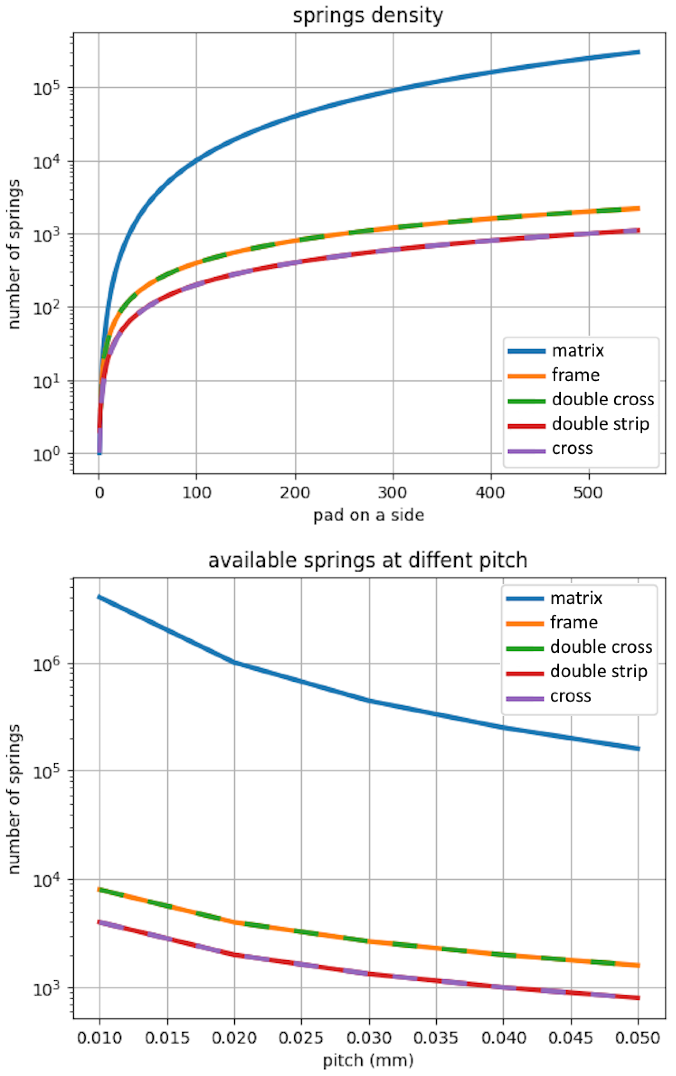
The design of the pad layout is of great importance [26] in the creation of a wafer probe station. The pads can come in different configurations, each with specific characteristics that make it more or less recommended based on various needs. Before delving into analyzing the other layouts, Figure 2 shows two graphs showing the five main layouts used on the die to expose the internal signals. The first graph shows the relationship between how many pads can be placed on one side of a die and how many springs will have to be used for the test. However, in the second graph, an inverse relationship occurs: given the number of springs, the pitch is obtained, understood as the distance between two adjacent pads of the pads on the dies. Based on the analysis illustrated in Figure 2, the five pad layouts examined can be grouped into three distinct behavioral categories. The first group, called Conventional Layouts, is composed of the configurations cross and double strip, which exhibit similar performance trends; in the second group, called Enhanced Layouts, the layouts double cross and frame yield a different yet internally consistent response; and in the third group, the layout matrix stands alone with a uniquely distinct behavior. Although the geometric differences among pad configurations might appear subtle, the resulting performance curves reveal that even these minor variations have a meaningful impact on the testing process, thus justifying this data-driven classification.
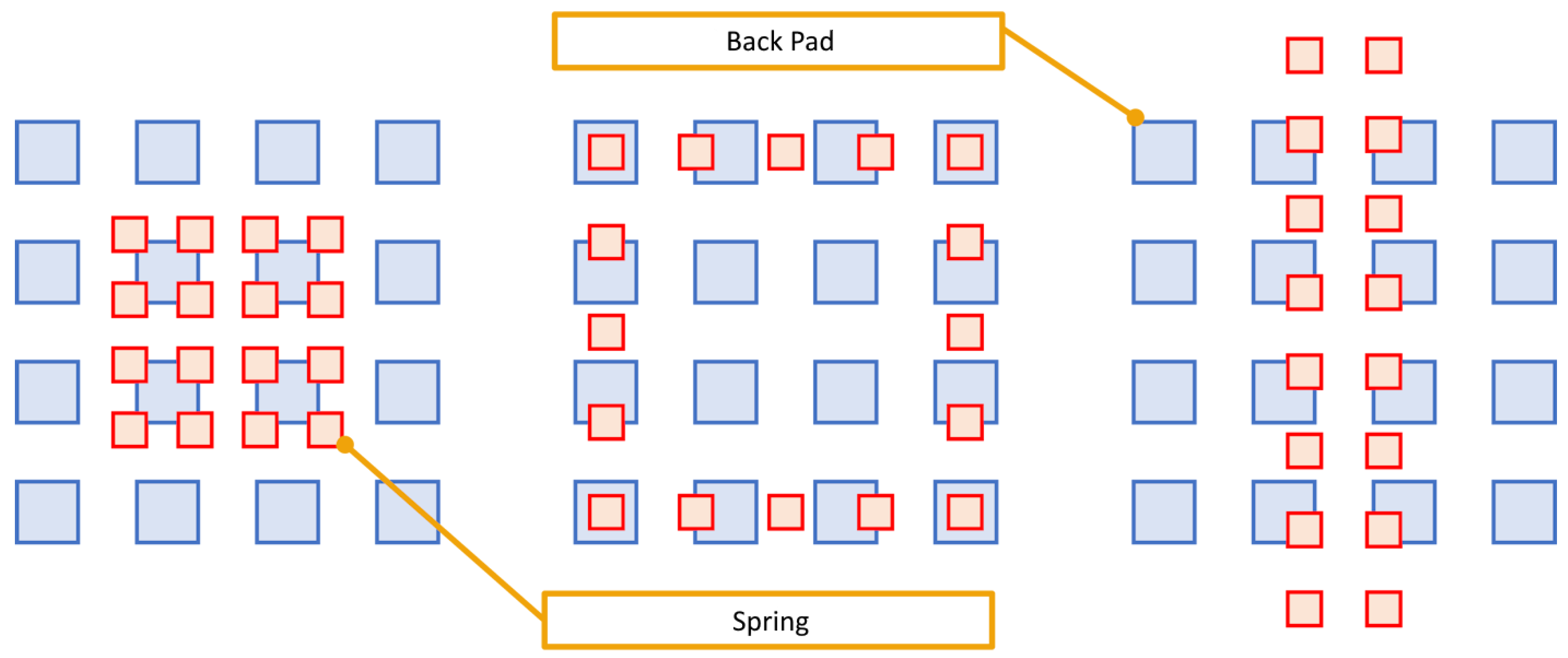
The first class (Conventional Layouts) composed of cross and double strip, represented in Figure 3 as the first and second pictures, also corresponds to the more traditional layouts. These configurations were used at the dawn of wafer testing because they are straightforward to create, check their alignment, and unravel the signals, because they have a limited number of pads from which they expose the test signals. Despite their simplicity, the small number of pads significantly reduces the speed at which tests can be performed.
As chips have evolved and become more complex, for testing chips while maintaining a sufficiently short test time, inserting more pads on the dies has been necessary. The increase in the number of pads was also linked to a decrease in pitch, so more pads could be inserted inside a die whose dimensions remained unchanged.
The use of increasingly developed technologies for alignment techniques has allowed smaller and smaller pitches to become possible [27], allowing for a higher density of pads. This has also led to the creation of more complex layouts, such as those belonging to the second class (Enhanced Layouts), double cross and frame, as seen in Figure 3 as the third and fourth pictures. These layouts enable higher test speeds due to the increased number of available pads. However, the precise alignment of the probe head is crucial to ensuring accurate contact and avoid signal integrity issues. To date, this class represents the de facto standard of the industry.
However, the third class shown in the fifth picture in Figure 3 is represented only by matrix. It is a design subject to intense debate. Its development was driven by the industry’s demand for an increased number of pads, with the aim of enhancing the testing efficiency at the wafer level and to accommodate the growing complexity in semiconductor manufacturing. This layout uses the entire die surface to expose the internal signals, but introduces a considerable problem. On a technical level, it is challenging to ensure the correct alignment of the innermost springs [28]. Even verifying that electrical contact has occurred between the spring and the pad is problematic; if it is not possible to verify the contact, a false negative can be generated, and the chip will be defective even if it is not.
Although one of the motivations behind the introduction of BGA and more complex pad layouts is to accelerate wafer-level testing, the main function of pads remains to provide functional access to the internal signals of the chip. In practical designs, it is uncommon for dedicated test pads to be added solely for wafer testing; rather, existing functional pads are often reused as test I/Os through time multiplexing. Moreover, while the wafer probe station serves as a critical platform for aligning and connecting the wafer via the probe card, it is the ATE that actually drives the stimulus signals and records the responses from the DUT. This distinction underscores that improvements in pad layout are implemented not only to achieve faster testing but also to satisfy the inherent need for robust functional accessibility.
Contrary to what one might think, increasing the number of pads on the die is not a definitive solution for wafer-level testing. Although more pads can reduce test time, their placement must be carefully managed. With ’pads over active’ technology, the reduction in usable surface area is no longer a limitation, but increasing the number of pads still presents challenges. A higher pad density makes precise probe alignment more difficult, and as the pitch between pads decreases, this can introduce significant technological hurdles in manufacturing and testing.

2.3. The Multi-Touch Approach

Until now, we have outlined multiple layouts of springs, disregarding how the springs are connected to the wafer probe station [29]. As introduced previously, the signals on the dies are exposed through the pads. Pads have been brought closer together and have increased in number as wafer test technology has progressed. However, their proximity has introduced considerable difficulties [30]. If, on the one hand, this allows a greater quantity of signals to be exposed, on the other hand, it is complex for the ATE system to access them. To solve this problem, an operation as delicate as necessary occurs inside the probe card: unraveling the signals to increase their pitch. The wafer probe station can contact and test the chips more efficiently with a larger pitch.
For all layouts, the back side of the probe card features a full matrix layout with enough contact points to accommodate all the springs. The choice was made to arrange the pack pads as a matrix, as this layout is the best for the physical space occupied. To date, the arrangement of the pack pads can vary depending on how the probe card is designed, but the matrix arrangement remains the most efficient.
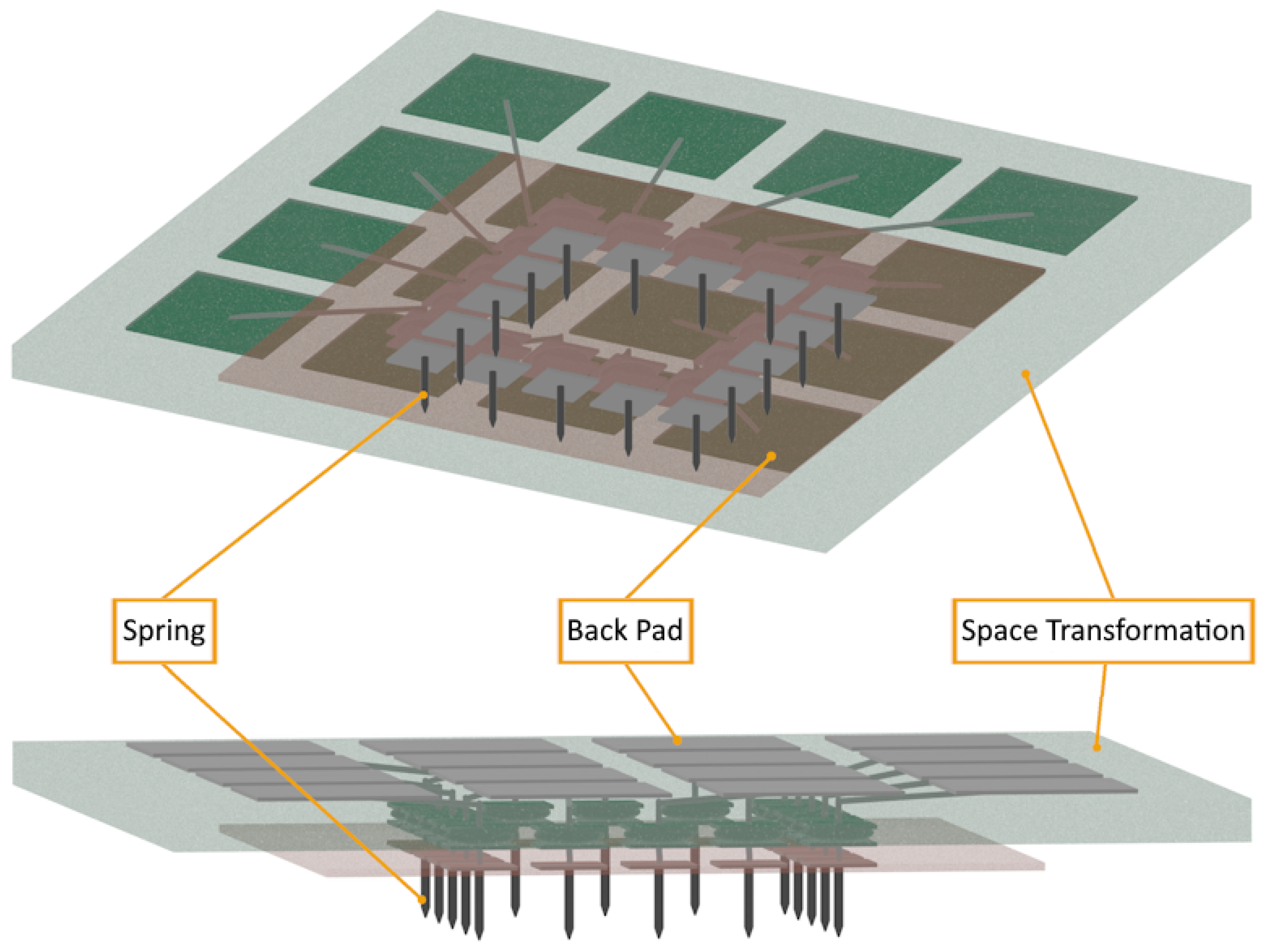
Figure 4 depicts a traditional probe head that belongs to the vertical probe card domains, which are the main focus of this paper. In the figure, you can distinguish the components described previously (Section 2.1). In particular, you can see how the springs cover a smaller area than the area used by the probe card; this is due precisely to the space transformation whose task is to unravel the signals and make them available again on the back pads of the probe card. As mentioned above, such equipment allows only one die to be tested simultaneously. For each wafer die, it is necessary to realign the probe head with the following die before the test can be performed.
Given the increasing complexity of devices and the growing demand for production, the need for faster testing methods has become paramount. This has led to discussions about the multi-touch approach, which involves a single probe head equipped with a carefully arranged set of springs. This configuration allows multiple dies to be tested simultaneously through a single contact action with the wafer, optimizing efficiency.
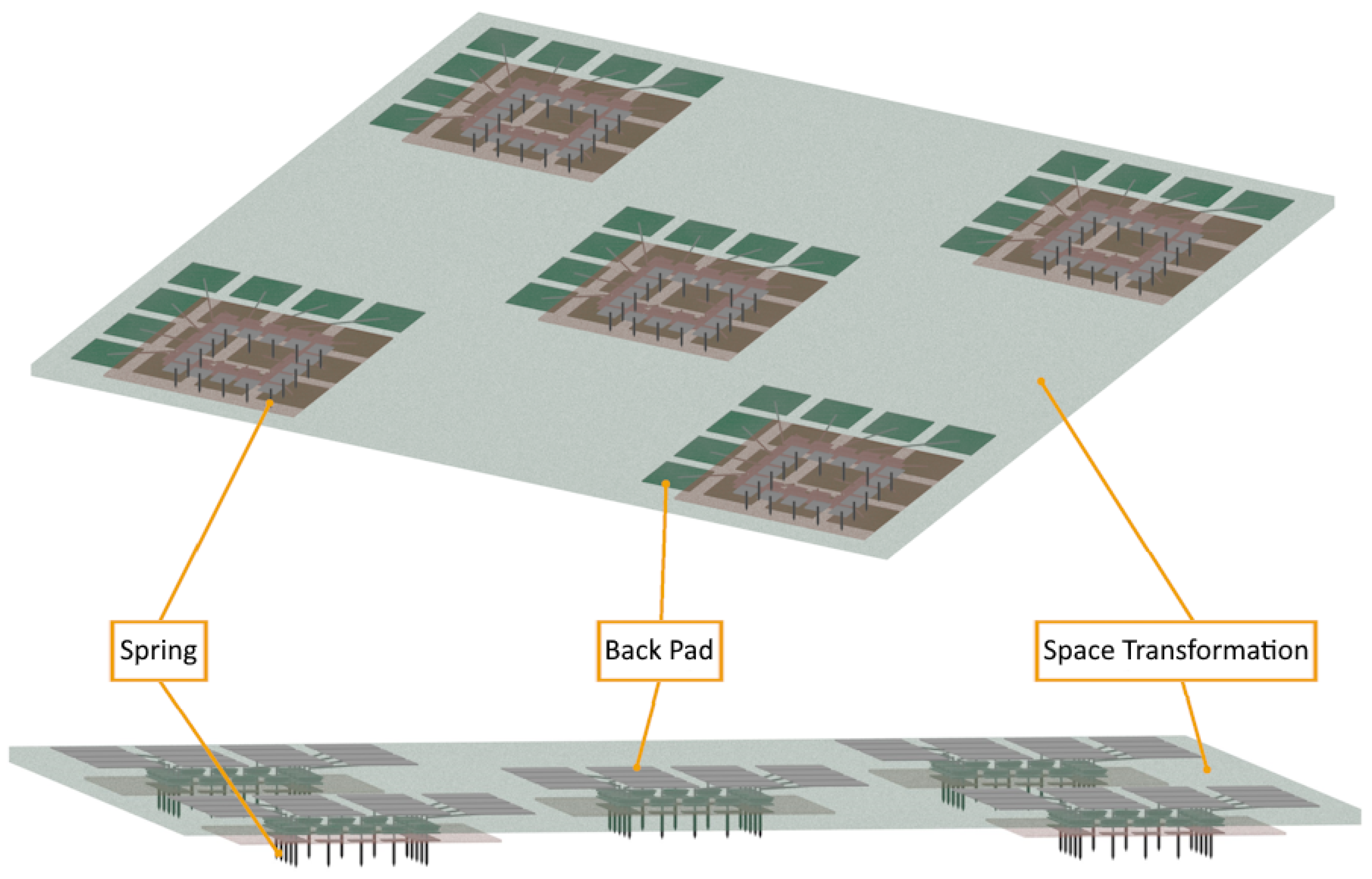
Figure 5 shows an example of a multi-touch head probe. Notice how five different sections have been created within a single probe head; each of these allows, through a single touch, contact to be made with a different die on the wafer, significantly reducing the time needed to test the entire wafer. How the dies come into contact with the wafer is of great importance in the case of multi-touch because the feasibility of this approach depends on this. The conversion rate between the springs and the back pads is one of the fundamental values to control for, as if this rate grows too much, the spatial occupation of the back pads could grow to the point of making it impossible to use a multi-type approach touch.
The shift toward multi-touch probe heads for wafer testing introduces several critical technical challenges that must be meticulously managed to ensure robust test performance and high production efficiency. One of the primary concerns is the increased number of probe card pins required per DUT. As testing multiple devices simultaneously demands a denser array of contacts, the probe card design must be optimized for efficient signal routing while preserving signal integrity across all channels.
Equally important is the physical footprint of the probe card. Enlarging the area to accommodate multiple test sites can impose mechanical constraints and complicate the alignment process. Maintaining a flat, well-aligned contact surface is paramount to ensure the repeatability and accuracy of tests. Any expansion in the probe card’s application area must, therefore, be balanced with design strategies that mitigate potential issues related to stability and durability.
In addition to the physical layout, the signal bandwidth in a multi-site testing environment becomes a crucial aspect to consider. The challenges associated with transmitting high-frequency signals through dense and often lengthy interconnects can lead to issues such as signal degradation and crosstalk. Optimizing the layout and routing of the probe card is essential to maintaining the desired frequency response and minimize interference, ensuring that the performance of each test channel is not compromised.
Furthermore, achieving high parallel test efficiency is vital. The potential throughput gains from testing multiple DUTs at once are significant; however, this benefit can only be fully realized if the system is capable of precise synchronization and effective thermal management. The coordinated control of the contact mechanisms, along with an intelligent test sequencing protocol, plays a crucial role in capitalizing on the advantages offered by the multi-touch approach.
In summary, while the multi-touch method promises substantial reductions in testing time and significant improvements in productivity, its successful implementation hinges on overcoming these intricate technical challenges. Future research should focus on developing innovative design solutions that enhance scalability, mitigate interference issues, and optimize both the mechanical and electrical aspects of multi-touch test setups, thereby ensuring high fidelity and reliable operation in demanding production environments.

3. Results

This section will outline our approach to developing an application for modeling the costs associated with creating and constructing a probe head. We will begin by discussing considerations related to the area occupied by each probe head. In addition, we will explore the feasibility of implementing a full-touch approach to test dies on the wafer. This full-touch method could accelerate the wafer sorting process [31] by introducing a significant speed-up. Next, we will introduce the concept of a horizon, which consists of a set of parameters to enable the full-touch approach. Subsequently, we will perform a detailed cost analysis for a specific configuration, considering the area occupation discussed earlier and the wafer-level testing process. Our parameter selection aims to closely resemble real-world scenarios, ensuring meaningful results. The choice of using arbitrary parameters was made not to depend on the production data of a specific product. The data used were obtained on the basis of the most advanced products on the market today. In this way, the results presented in Section 4 can be used to preview the marked today and, if necessary, make modifications according to one’s needs if one wants to study a specific product in more detail.
Given a target probe head technology, we want to estimate the cost of the wafer sorting step. To do that, we have considered the complexity of manufacturing the probe head, the cost of running the testing procedure, and the possibility of simultaneously performing multiple touches of the dies on the wafer while exploiting various probes. We produce a model that can help guide the selection of the best testing setup to minimize the cost.

3.1. Computation of Area Occupation

The first purpose of our system is to assess the probe head’s spatial occupancy. The distance between two springs, the desired space on the back side of the spatial transformation device to rapidly test the chip, and the arrangement of the springs in the probe head are the main determinants of this occupation [32].
Starting with the distance between springs, commonly called front pitch, the exact distance between the center of two adjacent pads inside a die is widely called pitch. In cases where it decreases below the ∼50 μm threshold, this distance represents a technological limit to test the chip [33].
As mentioned, the signals taken from the springs are subjected to disentanglement through the space transformation and reported on the back pads. Here, the back pitch is defined as the distance plus the diameter between two back pads in the upper part of the probe head. The pads in this area are the points from which the wafer probe station can inject and extract the signals.
To show the relationship between the front pitch and the back pitch, we have defined fb_ratio with the following formula:
f b _ r a t i o = f r o n t _ p i t c h b a c k _ p i t c h
The ratio represents the transformation rate that occurs within the space transformation. The above formula considers two critical aspects of the arrangement of the back and front pads. With regard to the back pads, it was decided to use only the matrix arrangement, as this minimizes the space occupied by the probe head. Given that this measurement is of considerable importance in determining the final surface of the probe card, it was decided to use the most efficient layout possible to carry out studies on the feasibility of the multi-touch approach. As far as the design of the pads [34] on the dies is concerned, this cannot be selected a priori, as this strongly depends on the construction and implementation choices [35], which, in some cases, must be addressed [36].
Since the layouts on the dies can be of different types, conducting a more in-depth analysis of each of these layouts is necessary. That is a crucial step because it allows us to understand how many probe heads can fit on the size of the wafer. Fortunately, as seen in Section 2.2, it is not necessary to perform analyses on all layouts but only on the three classes most widespread at a commercial level today. Figure 6 visualizes how, even with a fixed number of springs, different layouts can widely impact the area occupation of the device’s front side. In the image, the back pads represent functional pads which double as test I/Os.
Let us define the variables we are going to use to calculate the number of springs that a certain design can handle, given the area of the die to test:
1.
n_springs: The number of springs that can be distributed on the desired die.
2.
pitch: The distance between two test points (given in mm) and, by extension, the distance needed between two springs.
3.
chip_side: The size of the die (given in mm). For simplicity’s sake, we assume the die to be squared, but the same calculations can be extended to a die of any shape.
4.
fb_ratio: The ratio between the pitch and the distance between two pads on the opposite side of the space transformation device.
As we can see, the members of each class will behave very similarly, and the first and second classes will have an analogous trend. Only the third class will significantly change the behavior of our analysis.
Figure 3 pictures one and two show the layout of the springs of a double-strip and a cross probe head. The following equations describe the number of springs in contact with a given die if the probe head follows the layout of a simple cross and double strip.
n _ s p r i n g s c r s = c h i p _ s i d e p i t c h 2 1
n _ s p r i n g s d s t = c h i p _ s i d e p i t c h 2
The advantage of these layouts is that they are the simplest to monitor: a few vision devices are needed to ensure that the springs are correctly aligned and not damaged during testing. Having free space on the probe head also allows for the widening of the gap between the two spring rows, making it possible to place the contact points on the chip in more suitable positions.
With a fixed fb_ratio, we can approximate the maximum number of springs on the front side before the backside starts requiring less area than the chip itself. This critical threshold, which we refer to as horizon, is derived by equating the function that represents the area of the front side with that of the back side and then solving the resulting equation. Through the algebraic manipulation of this equality, the following analytical expression is obtained:
h o r i z o n c r s = h o r i z o n d s t = f b _ r a t i o 2 f b _ r a t i o + 1 + f b _ r a t i o f b _ r a t i o 2 2 f b _ r a t i o + 2
This formula results from the resolution of the equation that balances the cost (or area) contributions from both sides of the device. Essentially, it serves to pinpoint the critical point at which further additions to the front side no longer result in an effective use of the chip’s area, thereby marking the optimal trade-off between the two regions.
Moving to denser configurations, Figure 3 pictures three and four show the layout of the double-cross and frame probe heads. The following equation describes the number of springs in contact with a given die if the probe head follows the double-cross or the frame layout:
n _ s p r i n g s d c r = n _ s p r i n g s f r m = ( c h i p _ s i d e p i t c h 1 ) 4
Although the layouts differ from the previous ones, the number of springs that they can host does not change drastically. The two proposed layouts can only accommodate double the number of springs in the earlier designs. Once again, the addition of more springs does not come without costs [37], and to fully monitor these configurations, we would need multiple vision devices. The double-cross layout allows one such device to be hosted in each corner to inspect the probe head’s correct functioning thoroughly. In contrast, the frame configuration hosts a single free region in the center of the probe head. This would allow for the installation of more area-demanding control chips but simultaneously has to contend with the space required for the vision devices to be installed.
Once again, we can also approximate the horizon for this kind of layout:
h o r i z o n d c r = h o r i z o n f r m = 2 f b _ r a t i o 2 f b _ r a t i o + 1 + 2 f b _ r a t i o f b _ r a t i o 2 f b _ r a t i o
Lastly, Figure 3 picture five shows the layout of a full matrix probe head. Such a probe head is extraordinarily dense and allows for unparalleled bandwidth during testing.
n _ s p r i n g s m t x = ( c h i p _ s i d e / p i t c h ) 2
As the above equation highlights, the number of springs in this configuration scales entirely differently from before. While the other layouts had linear scaling, a full matrix has springs that are quadratically proportional to the length of the side of the single die. This change is significant because it makes it impossible to find a horizon point.

3.2. Formulation of Probe Head Cost Analysis

The approach we propose proceeds with the calculation of the cost relating to the creation of a probe head. This cost is quite complex but depends on two main factors.
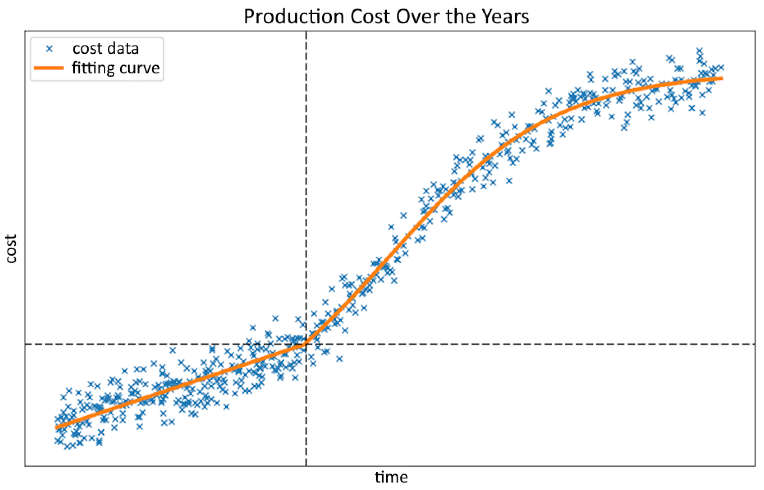
The first factor that influences the cost of a probe head is the pitch between two springs, which is directly impacted by the technology used for the printing machines. A lower pitch would require a significantly newer machine [38], so the cost of a given device would increase significantly. The cost associated with this factor was obtained in such a way as to consider that each technology tends to decrease in price over the years with a more or less abrupt but essentially constant trend. At the same time, the use of cutting-edge technologies today costs significantly more than when they are adopted at a commercial level. This led us to obtain a function for estimating the cost due to the use of different types of pitch. The approach distinguishes between the economic trajectories of mature and emerging technologies, based on both economic phenomena and market dynamics.
For products based on older technologies, a linear function is chosen to model the evolution of the cost over time. The underlying assumption is that production processes are well established; economies of scale have been fully exploited, and production methods have reached a level of maturity where cost variations occur at a relatively constant rate. In this scenario, depreciation or cost reduction can be uniformly predicted over extended periods and modeled effectively with a simple linear function, where the slope corresponds to the average constant rate of cost decrease brought about by incremental improvements and optimizations.
In contrast, for future technologies or those at an early stage of diffusion, a sigmoidal (S-shaped) curve is used to capture the cost dynamics. This model inherently reflects three distinct phases: an initial phase where the cost remains high and almost invariant due to significant research, development expenses, and challenges in scaling up production; a subsequent stage characterized by a rapid decline in costs as production processes are refined, economies of scale are realized, and efficient manufacturing techniques are adopted; and finally, a mature phase where cost reductions stabilize and further improvements yield only marginal gains. This typical pattern, slow initial progress, rapid transition, and eventual saturation is naturally described by an S-shaped curve.
The selection of these models is not arbitrary but is based on empirical analysis of data from various products. Data for mature technologies align well with a linear trend, probably because the annual depreciation or innovation rate translates into a uniform impact on overall cost. In contrast, emerging technologies exhibit cost variations that cannot be adequately described by a simple linear model; instead, the sigmoidal model captures the transition from high initial costs to a rapidly declining cost phase, followed by stabilization as the technology matures.
This dual-model approach has significant implications for both economic evaluation and market strategy. Although the linear model offers a predictable and constant cost estimate for mature products, the sigmoidal model provides valuable insights into key milestones in cost reduction during the innovation phase. Such insights can help determine the optimal timing and strategy for investments in new technologies, ensuring that financial commitments are synchronized with the potential for cost savings once the initial development stage has been surpassed. In Figure 7, it is possible to observe a representation of this curve, while the equations used for the calculation are as follows:
y = m x + c + K { < x < 0 } y = K x = 0 y = e x K 1 + e x K { 0 < x < + }
The second factor that enormously influences the cost of a probe head is the number of springs that have to be printed; this represents a significant factor since most probe heads are produced through a printing process, and increasing the number of springs to be used would directly influence the time required to complete the product itself along with increasing the general complexity of the probe head [39]. It should also be remembered that a more significant number of springs corresponds to a more outstanding spatial occupation of the probe card, reducing the number of probe heads deployed on a single wafer probe station. Therefore, as the number of springs increases, the cost of the printing equipment needed will grow linearly with the number of springs that the designated probe head possesses. However, at the same time, as the number of springs increases, a cost component is influenced by the number of probe heads that can be deployed. Each probe head has its own production cost, which is not insignificant but allows for a drastic reduction in the time required to carry out the test operations. Therefore, using a multi-touch approach introduces the need to identify a minimum point relating to how many probe heads one can use. Since increasing the number of springs in our design could incur an enormous cost, we must motivate this choice. As demonstrated by Mottaqiallah et al. [8], increasing the number of springs on our device would also increase the bandwidth for the testing phase. Since operating a testing machine is a considerable cost, reducing the time spent in this phase would increase the throughput of chips and significantly reduce the operation costs.
To determine the cost of a probe head, it is also necessary to consider the production chain, which is essential to creating everything a device requires. Since the modeling of this process is familiar, having been covered in several articles (see [3,22,23]), this value is assumed as a constant variable and named within our formulas as reference_head_cost. Briefly summarizing what this parameter represents, it considers the costs of materials, transport, assembly, ordinary and extraordinary maintenance, and many other parameters concerning the production chain.
h e a d _ c o s t = r e f e r e n c e _ h e a d _ c o s t r e f e r e n c e _ p i t c h e x p e c t e d _ p i t c h
With fixed cost for each probe head, we could focus on the number of probe heads that simultaneously touch the wafer, proportionally reducing the duration of the whole procedure. Having selected a layout and pitch for our springs and an fb_ratio, we can compute the upper limit of probe heads that we can fit on a single wafer.
Following the discussion, we must determine the number of chips that a wafer can host. Then, we need to define some information regarding the characteristics we require for our probe head, particularly the number of touches it can perform before maintenance and the pads’ pitch on the probe head’s back side.
Once we have performed this, we conduct a simulation to compute the number of steps that the procedure will have to perform to ensure contact with all the chips on the wafer. Then, for any number of probe heads lower than the upper limit, we repeat this calculation to understand whether or not adding more probe heads is valid or if we are adding redundant devices that only increase the overall cost.
As a last step, we define a reasonable number of touches that a given probe head can perform before being damaged due to the stress of the procedure [40]. If we can perform a full touch, the number of touches a probe head can perform is equivalent to the number of wafers that the testing equipment can produce before requiring maintenance. Therefore, reducing the number of probe heads increases the time to test a wafer and reduces the number of wafers tested between two consecutive machine maintenance cycles. As we have already discussed, to perform a full touch of our device, we need as many probe heads as there are chips to test. We must refer to the calculations in Section 3.1 to do so. The front–back pitch ratio and layouts greatly influence the area that such a device occupies. In particular, achieving a full touch with an entire matrix layout is possible only when fb_ratio = 1. That is, no spatial transformation is applied. The inability of a full matrix to achieve a full touch is highly detrimental, and although it can offer an enormous bandwidth for testing, requiring multiple touches on the same wafer adds both moving time and reduced lifetime for the probe head itself.
The following section will use this information to approximate the test cost per die.

3.3. Evaluating Cost per Die

To obtain the cost of testing a single die, it is necessary to initially abstract it to obtain the overall cost of the entire testing procedure. The total cost can be divided into two factors that contribute to its value, as seen in the following formula:
t o t a l _ c o s t = h e a d s _ c o s t + l i f e c y c l e _ t e s t _ c o s t
The term heads_cost represents the overall cost of the probe heads used. All expenses related to the design, transport, materials, and construction of a probe head are included in this value. This value was obtained by multiplying the cost of the single probe head, seen in Section 3.2, by the number of probe heads chosen. The number of probe heads chosen was calculated in such a way as to minimize this cost.
The second term, lifecycle_test_cost, represents the cost associated with the test. This takes into account aspects such as the hourly cost of using the wafer probe station, the overall time to perform the test operations, the maximum number of touches that a spring can perform before it needs to be replaced, and the cost of performing ordinary maintenance in a particular way to clean the springs [41]. We, therefore, introduce cost_of _testing as a parameter to calculate the cost associated with the test. As can be seen in the formula below, for its calculation, the number of touches necessary to test an internal wafer is used [42], as well as the time required to execute a specific test and finally a cost that includes what was introduced previously.
c o s t _ o f _ t e s t i n g = n u m b e r _ o f _ t o u c h e s t i m e _ f o r _ t e s t i n g m a c h i n e _ c o s t
However, the above formula lacks some of the characteristics of lifecycle_test_cost; for this reason, cost_ for_moving was introduced. This term quantifies the time required for the probe head to realign itself on one or more dies, a critical factor in non-multi-touch approaches, where for wafers of considerable size, the probe head must be realigned for each individual die.
Furthermore, the cost of testing should include factors such as the overdrive value during probe card contact and the ensuing cleaning cycle, which are necessary to ensure a reliable electrical connection and maintain probe performance. In our model, the parameter time_ for_moving incorporates not only the pure mechanical repositioning time but also the additional time needed to fine-tune the overdrive. Simultaneously, the multiplier machine_cost is adjusted to include the cost burden associated with the cleaning cycle after each contact and also the associated cost to operate the machine.
c o s t _ f o r _ m o v i n g = t i m e _ f o r _ m o v i n g ( n u m b e r _ o f _ t o u c h e s 1 ) m a c h i n e _ c o s t
We can now obtain the formula representing the lifecycle_test_cost with these last two formulas. This formula is the sum of the previous two, in which the number of touches is considered to test all the dies on a wafer and the maximum number of touches before a spring must be replaced.
p r o c e d u r e _ c o s t = c o s t _ o f _ t e s t i n g + c o s t _ f o r _ m o v i n g
l i f e c y c l e _ t e s t _ c o s t = p r o c e d u r e _ c o s t m a x _ t o u c h e s n u m b e r _ o f _ t o u c h e s
Therefore, the total cost can be obtained by the sum of lifecycle_test_cost and heads_cost. It is possible to estimate the cost of a single die by using the overall cost and dividing the value obtained by the number of dies to be tested on the wafer. The calculation of the chip cost is as follows:
c h i p _ c o s t = l i f e c y c l e _ t e s t _ c o s t + h e a d s _ c o s t c h i p _ a m o u n t
In the following section, we will discuss an experimental evaluation of the formulas just described over the lifetime of the probing device, trying to highlight potential configurations that would provide an optimal relation between the cost of the testing and that of the device itself.

4. Discussion

This section presents the case study and will be divided into three operational parts. Initially, the simulation of the area computation will be treated. Subsequently, the graphs relating to the cost of a single die will be presented. Finally, a tool suite that is used and usable for wafer test cost modeling will be given.
At the beginning of the case study, Jupyter Notebooks were used to carry out the first tests and checks on the functioning of our calculations. Subsequently, after evaluating and ascertaining the platform’s functioning, it was decided to migrate the environment and provide it with a dedicated graphical interface to make it easier to use. The cost results and graphs reported later were calculated with the help of these tools. The tool used to obtain the results presented in this section considers the concept of multi-site, a probe head capable of testing multiple dies simultaneously with a single touch. When modeling the tool, we assumed that each die on the back side was created as a matrix instead of merging all the pads available on the back side into a single matrix. This choice will be subject to changes in subsequent versions of the tool.
Within the tool, we used arbitrary values, decided by us so that the order of magnitude used is by the standards of the products on the market today, but at the same time, not directly attributable to any specific product. This choice allowed us to have a tool that could be used for particular products if necessary. Furthermore, the results reported here, having been calculated with data representing the current products, are generic and can be used as a first source of comparison to highlight the current situation on the market regarding wafer testing.
The case study presented later was modeled by using various parameters. In particular, the values were 20 mm for the die side, 12 inches for the wafer diameter, a ratio of 10, and a maximum of 1,000,000 touches for a single probe head.

4.1. Simulation of Area Computation

In this section, we will develop the methods explained in Section 3, calculating experimentally the front and back areas of each spring configuration, and show how the respective curves intersect, highlighting where the space required to host all the springs is larger than the area to host the back pads.
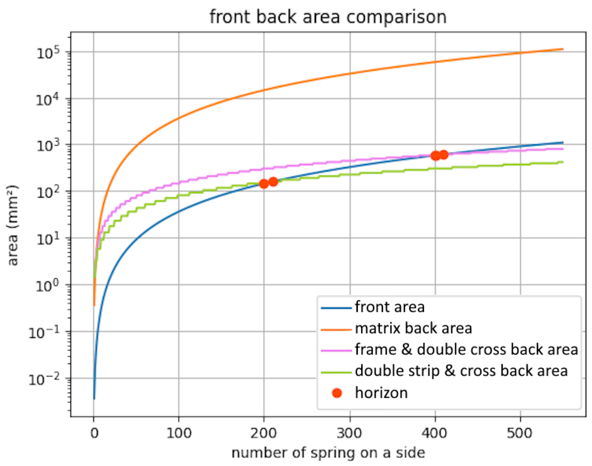
Considering the double-strip and simple-cross configurations, in Figure 8, we can see a blue curve that follows the increase in the area of the front side of the device depending on the number of springs. The green curve shows a stair-like behavior since we approximated the layout of the back pads as a full matrix that increases in size only when there are not enough pads present to connect to each of the springs. As shown in the formula in the previous section, the back side of the device takes advantage of a more efficient layout and quickly reaches the point where the front area is larger than the back. It is important to note that in this simulated example, more than one horizon point exists due to the stair-like trend of the orange curve.
Figure 8 shows also the exact behavior for the double-cross and frame layouts. Also, in this case, the pink curve presents a stair-like behavior due to the entire matrix arrangement of the back pads. Although the horizon is shifted to the right of the graph, the curve follows the same trend as the previous one. As has already been discussed in Section 2.2, the behavior of this second class remains similar to the performance of the first class, despite a relative improvement possible due to the better technologies adopted, such as pitch reduction and the use of more advanced layouts that allow multiple pads to be placed on one die.
As already noted through the formulas, contrary to the previous examples, the full matrix layout makes it impossible for the space transformation device to fit entirely in the same area of the springs. As a result, we cannot avoid multiple testing steps to make contact with every chip on the wafer, given the area occupied by the device. The matrix curve in Figure 8, which is colored orange, does not show the step-like behavior highlighted above, since the back size increases like the front area, given that the layout is the same on both sides. The layout is not suitable for performing a full touch because there is no horizon point.
Assuming that we vary the front area, observing how the different classes react in the space necessary to accommodate the back pads required to execute the tests by the wafer probe station in the back area is possible. The three classes in the image (green, pink, and orange lines) are distinguishable. In particular, note that with the same number of pads on a die, the necessary back area increases as the class you intend to use increases.

4.2. Experimental Evaluation of Test Cost per Die

In this subsection, we discuss the practical application of the calculations and formulas derived in Section 3.2 and Section 3.3. The insights gained during this phase enable for a comprehensive evaluation of test costs at the wafer level. Using our advanced tools, we can effectively minimize these costs by selecting optimal parameters to design a highly suitable probe head.
Furthermore, the configuration constraints are explicitly considered in our calculation model. We analyze several layout configurations, including an N-site diagonal, a 1 × N linear arrangement, and a checkerboard pattern, and then select the most cost-effective design. This approach demonstrates that our model is generally applicable and well suited to various configurations, rather than being limited solely to specific cases.
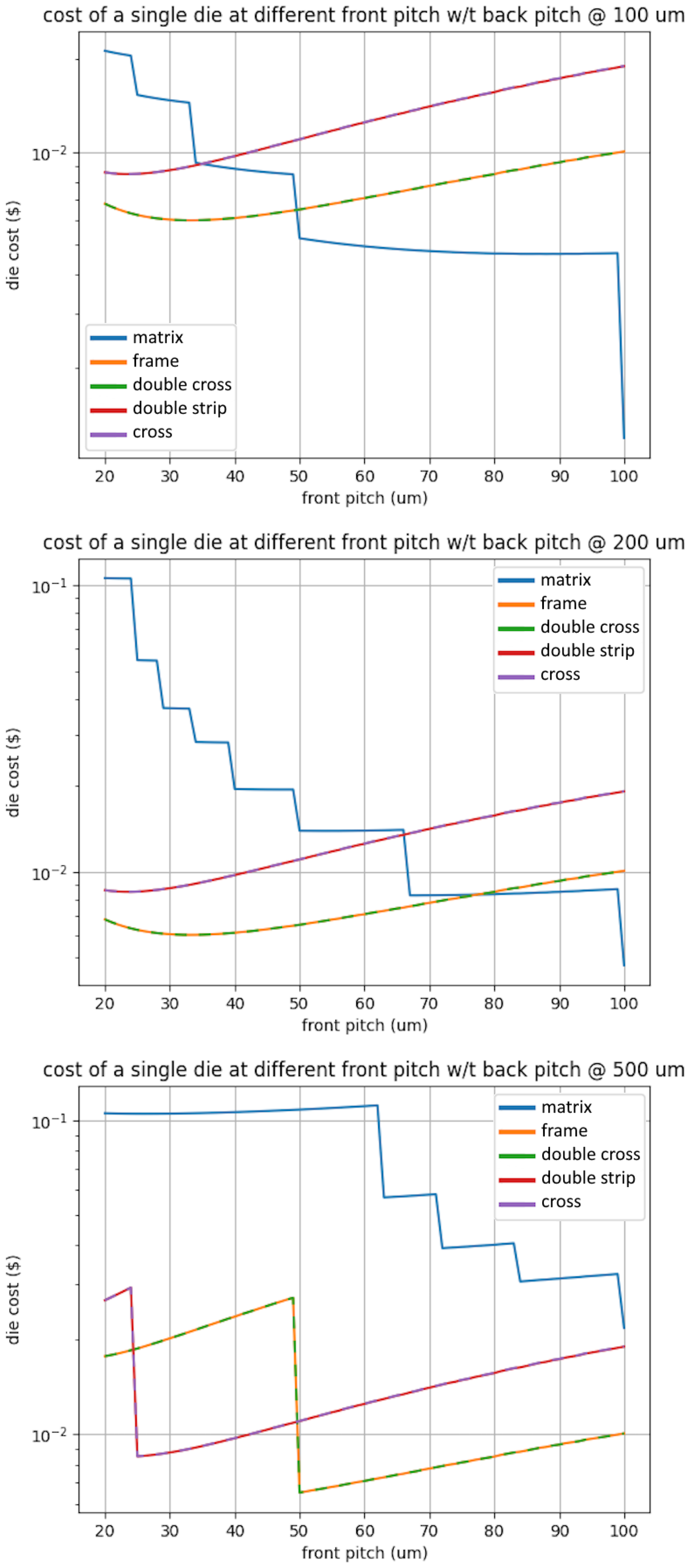
In Figure 9, we show the evolution of the test cost for a single die, first calculating the overall cost and then spreading the cost of the probe heads on each chip to test during the lifetime of the probe head.
The graphs obtained allow us to trace the cost trend of the single die, represented on the Y-axis, while the X-axis is dedicated to the front pitch. The front pitch is graphed within a specific interval, which depends on what technology is available for the creation of the pads and, consequently, of the springs, which will have to provide electrical contact with the die. Each graph also has a third variable, which remains constant in the graph, but through the tool, it is possible to set a series of values to which this parameter can be set to obtain different graphs, one for each value. The back pitch represents the constant parameter in the graphs. In addition, in this case, it is a value that substantially impacts the final cost. Still, compared with the front pitch, it presents fewer technological restrictions concerning creation, while the higher this value is, the greater the problems related to the feasibility of a multi-touch approach are, as the space occupation can be limiting and does not allow for the use of additional probe heads alongside the main one. This leads to a full touch, which becomes more demanding as the back pitch increases.
Following the last equation presented, the plot can be read as follows: The further we are on the left side of the plot, the smaller the pitch. As a result, we obtain a higher bandwidth during our tests, and the overall test cost is reduced. At the same time, the cost of the probe head increases because the technology to produce such a device is more innovative, and the number of springs to print increases. Furthermore, having more and more springs also increases the size of the spatial transforming layer and requires multiple touches to test all the chips. In contrast, the further we are on the right side of the plot, the more significant the front pitch. This provides the benefit of a more inexpensive probe head and a smaller front–back ratio, allowing more heads to fit on the wafer. The most significant downside is the increase in testing time for the single chip. Still, we must remember that the wafer’s overall testing time is reduced thanks to the possibility of hosting multiple heads.
Figure 9 represents three separate instances; in particular, it concerns the cost of testing a die with a front pitch that varies from 20 μm to 100 μm. The back pitch varies in the three graphs and is worth 100 μm, 200 μm, and 500 μm.
In the first and second of the three graphs, it can be observed how the first and second classes have almost similar trends apart from a slight inflection around 25 μm and 35 μm for the first and second class, respectively; it appears slightly inclined and tends to increase as the front pitch increases. The behavior changes when the back pitch increases and reaches 500 μm. The curves are subject to a sharp drop around 25 μm and 50 μm, respectively. At these specific points, the combination of factors that allow you to perform a multi-touch approach includes a particular ratio between the front and back pitch that guarantees the lowest cost to test a die at the wafer level. In case it is not possible to use technology for the creation of pads and springs with such front pitch value, it is always possible to compare these graphs to find a sub-optimal solution, this solution. However, the one with the lowest cost is not always competitive compared with an approach without studying the cost. Lastly, the third class, as already mentioned, is composed solely of the matrix layout. Today, it is of considerable interest to the industry, as it is an approach that guarantees an enormous bandwidth in a small space.
Still, difficulties are inherent in the approach, as this layout does not allow the traditional methods commonly used today to verify the correct electrical contact and alignment of the probe head on the die. For these reasons, the narrow pitch matrix approach tends to be incredibly expensive in all three graphs. It should also be remembered that the matrix approach can outperform other approaches and obtain an extremely high number of pads at the same pitch. For these reasons, the comparison should be made between the various classes, comparing low pitch values for the first two, while the third class can operate efficiently at higher pitches. It should also be taken into consideration that the simple use of a matrix approach allows you to save a lot of money, as it is not necessary to use advanced techniques for the creation of pads at reduced pitches, to the detriment of possible alignment or mechanical contact problems, which can be alleviated at the expense of a non-negligible financial investment. It is, therefore, interesting to observe when the matrix approach, which has a stepped behavior due to the use of a matrix for arranging the back pads, is more economical than classes one and two. This happens very quickly; in the first graph, the third class has a cost per day equal to the first class when this reaches 35 μm; by increasing the back pitch, the value reaches about 65 μm, while in the last graph, equality is reached shortly after 100 μm.
In the first of the three images, we can see that the full matrix layout manages to reach a full touch after the 100 μm front pitch, which, as already stated, is pointless, since at that point, we are completely avoiding the spatial transformation device. As the pitch after the spatial transformer increases to achieve the full touch, it is increasingly more challenging, and each time the device needs to perform one more touch, we see a steep increase in the cost per die, since it will get damaged before testing as many wafers as before. By increasing the back pitch even more, we see the same pattern applied to the more straightforward layouts, and the smooth plots start showing some dents.
Although our model assumes an ideal scenario for N-site testing, real-world factors significantly affect the achievable speed-up. In particular, wafers are inherently circular, whereas probe cards are typically designed in a rectangular format. This mismatch implies that dies located at the wafer edges cannot be fully exploited by the probe card, thus reducing the effective number of dies tested per touch. In other words, while the theoretical model anticipates a cost reduction by a factor of N, edge losses and the non-uniform distribution of dies lead to an effective testing factor lower than N. A potential way to account for this effect in future models is to introduce a geometric correction factor, η, with 0 < η < 1, which adjusts the nominal boost of the N-site to the speed.
Another critical factor affecting test cost reduction is the abort-on-fail mechanism. In single-site testing, this strategy enables significant time savings by terminating tests as soon as a failure is detected, thereby saving unnecessary test cycles. However, in an N-site testing scenario, the probability that all N dies fail simultaneously is considerably lower. As a result, even when most dies exhibit failure, the test must be completed for at least one functioning die. This diminishes the potential reduction in test time and cost that would be expected based solely on the factor of N speed-up. To quantify this, one could introduce a probabilistic model where if the probability of failure per die is ρ, then the likelihood of all N dies failing is ρN. When ρ is moderate or low, especially for N greater than 1, the abort mechanism loses efficiency, and the overall cost reduction is less than the idealized factor N.
The current cost model, while robust in capturing many essential aspects of probe head design and testing, does not fully incorporate the aforementioned geometrical and procedural limitations. Incorporating a geometrical correction factor and a more detailed probabilistic treatment of the abort-on-fail mechanism would undoubtedly lead to a more accurate prediction of the actual cost reduction achievable with multi-site testing. Future research will, therefore, focus on refining these aspects, possibly through experimental validation and the integration of real-world data, to better quantify the effective speed-up and cost savings.

4.3. Graphical User Interface for Cost Modeling

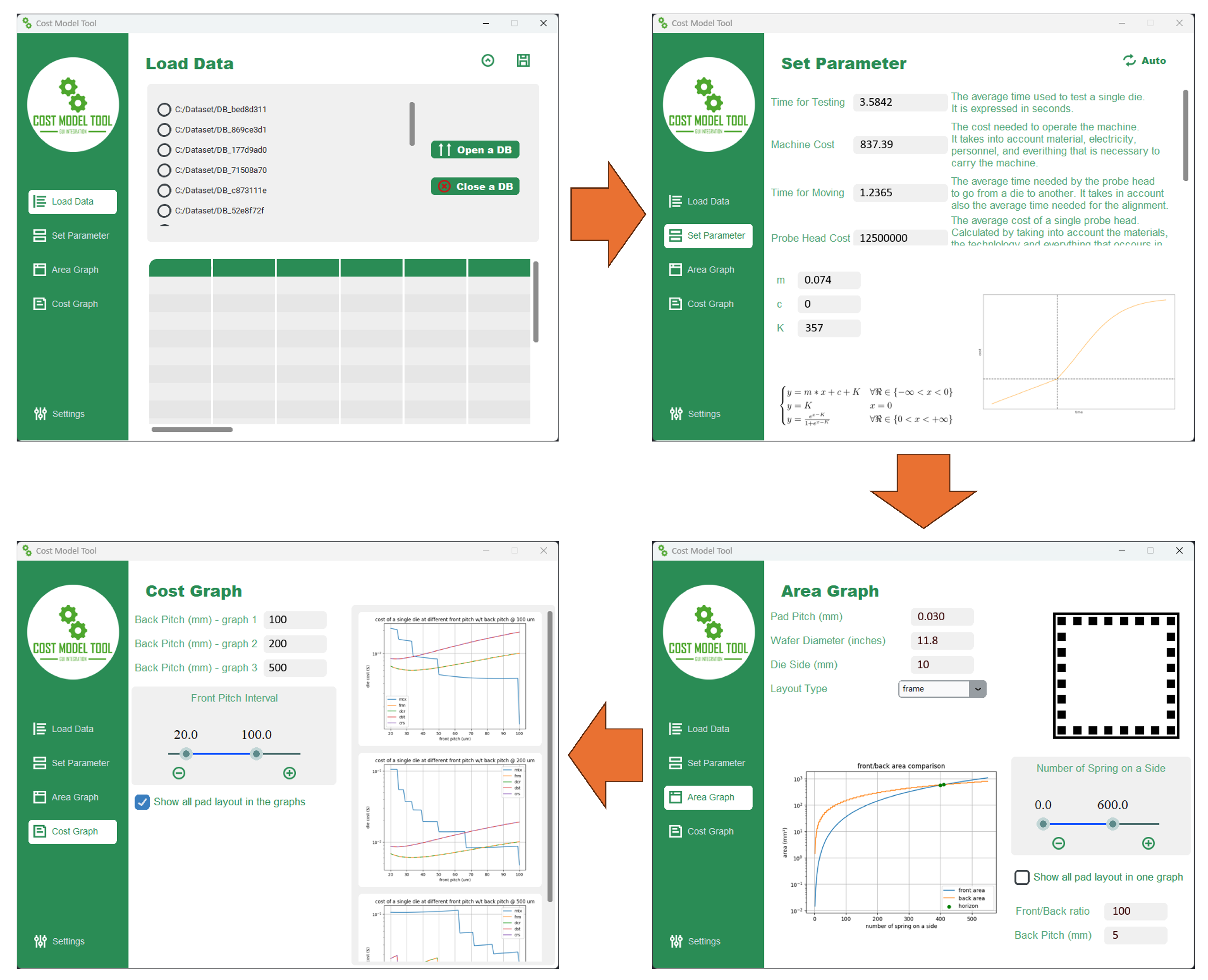
In this section, we present the graphical user interface developed to support the design of a probe head optimized for cost. The tool, which is based on the calculations and methodologies described in the previous sections, also benefits from the practical experience gained during the prototyping phases using the Jupyter Notebook environment. The GUI does not claim to introduce new research innovations; rather, it facilitates the transition from theoretical analysis to practical implementation, allowing for rapid experimentation and the validation of results.
The structure of the interface follows a sequential workflow that guides the user through the essential stages, with the possibility to intervene at each step to refine and verify design choices.
Initially, the data import module allows for the loading of production databases formatted according to predefined standards. This step is crucial because it ensures that the parameter calculations are based on reliable empirical data. The system automatically collects the necessary information by consolidating data from various sources and provides a concise real-time overview of the imported datasets.
The next stage focuses on the parameter configuration. Here, the interface offers an automatic calculation algorithm that, by analyzing the imported data, determines preliminary values for the parameters required for modeling. However, to allow for greater flexibility, in cases where the researcher already has precise information, the system also enables manual parameter adjustments. This dual mode of operation, automatic and manual, ensures that the model can be tailored to the specific requirements of different operating contexts, achieving an optimal balance between robustness and customization.
The third module is dedicated to defining the layout of the pad. In this phase, the user chooses among several predefined configurations (such as cross, double strip, matrix, etc.) and is provided with a real-time graphical representation of the layout on the die. Although visual feedback is kept concise, it is essential to immediately understanding the implications of the chosen option on space occupancy. This allows the user to evaluate and, if necessary, adjust the geometric setup to optimize the use of the available area.
Finally, the last section focuses on cost modeling. After consolidating the data flow and defining the spatial arrangement, the tool requires the entry of additional project specifications, such as the front and back pitch values, to generate graphs that depict cost trends as a function of the design choices. These visual outputs facilitate the comparison of different solutions and guide the user toward a configuration that minimizes the overall cost of the probe head. If the results obtained do not meet the established criteria, the iterative process enables the user to return to previous steps to modify the parameters and progressively refine the model.
In summary, the proposed graphical user interface serves a dual function: on the one hand, it simplifies the operational aspects of the design process by providing an intuitive and structured workflow; on the other, it ensures that every stage of the calculations and analyses is closely linked to real data and project requirements. Figure 10 offers a comprehensive view of the system, highlighting how the process moves from data import, through parameter configuration and layout definition, to the final cost evaluation. This integrated approach underscores the importance of combining automated processes with decisions informed by practical experience, thereby ensuring a reliable and versatile solution for the design of the probe head.

5. Conclusions

In this article, we explore the world of multi-probe wafer testing by examining various pad arrangements within chips on wafers. Our study provided valuable information on the technological constraints currently limiting the development of probe heads capable of testing chips with pad pitches smaller than approximately ∼50 μm. The investigation covered several pad configurations, including matrix, cross, double cross, frame, and double strip, which we subsequently classified into three distinct categories based on their performance characteristics. For instance, while the matrix configuration maximizes the number of springs, thereby potentially increasing testing throughput, it may become inefficient when there is a significant disparity between the front and back pitch. Furthermore, we developed a specialized simulation tool to compute these results, which stands out for its adaptability, as input parameters can be dynamically adjusted to reflect a variety of realistic manufacturing scenarios.
Although our simulation-based analysis offers a robust and informative framework, it is important to acknowledge the inherent limitations of relying solely on computational evaluations. Simulated environments, while invaluable for preliminary analysis, inevitably simplify complex interactions and may not fully capture the variability and unforeseen challenges present in real-world applications. For example, factors such as material inconsistencies, environmental variations, and unmodeled process noise can influence the performance of probe heads in ways that simulations might overlook. Recognizing these potential gaps, we see an essential need to complement simulated evaluations with experimental validations. Future research will focus on implementing experimental studies designed to verify our computational models and refine them further. Such studies would not only confirm the accuracy of our simulation data, but also provide deeper insights into probe behavior under genuine operating conditions.
While the multi-site approach theoretically promises a reduction in test time and cost, practical limitations, stemming from the circular geometry of wafers versus the rectangular nature of probe cards and the reduced efficacy of abort-on-fail strategies, lead to a more modest improvement. Future work will be devoted to refining the cost model by incorporating these limitations to provide a more accurate and comprehensive evaluation.
In conclusion, the article presents a novel framework aimed at expanding the conventional single-site testing approach by integrating a comprehensive analysis that includes both theoretical modeling and practical design considerations. By addressing the spatial constraints and technical challenges associated with pad arrangement on dies, our method deepens the understanding of current limitations and opens up new avenues for optimizing wafer-level testing. The iterative design process, supported by our simulation tool, allows researchers and practitioners to continuously refine probe head configurations and balance cost efficiency with performance. Ultimately, while simulations have provided a strong foundation for our exploration, we eagerly anticipate that forthcoming experimental validations will bolster the practical relevance of our work and lay the groundwork for its broader industrial application.

Author Contributions

Data curation, T.F.; Formal analysis, T.F.; Investigation, P.B. and T.F.; Methodology, P.B. and T.F.; Project administration, P.B.; Software, T.F.; Validation, P.B.; Visualization, T.F.; Writing—original draft preparation, T.F.; Writing—review and editing, P.B. and T.F. All authors have read and agreed to the published version of the manuscript.

Funding

This research study received no external funding.

Data Availability Statement

The data utilized in this article originate from authentic case studies, ensuring a high degree of realism and relevance to real-world scenarios. However, please note that these datasets, apart for the data already shown in the paper, are not accessible to the public audience due to confidentiality agreements and privacy considerations.

Acknowledgments

This article represents a substantial extension of the previous work “Exploring trade-offs in multi-site wafer testing”, published in the 25th IEEE Latin American Test Symposium (LATS), The conference reference is [43].

Conflicts of Interest

The authors declare no conflicts of interest.

Abbreviations

The following abbreviations are used in this manuscript:
ATEAutomatic Test Equipment
BGABall Grid Array
CMOSComplementary Metal–Oxide Semiconductor
DBDatabase
DIBsDevice Interface Boards
DPWDies Per Wafer
GUIGraphical User Interface
PCBPrinted Circuit Board

References

  1. Jiang, Y.; Chen, Y.; Hu, F.; Han, D.; Fang, J.; Li, G.; Ouyang, K. Solution to Optimize Warpage performance for 2.5D Fanout Packaging. In Proceedings of the 2023 24th International Conference on Electronic Packaging Technology (ICEPT), Shihezi, China, 8–11 August 2023; pp. 1–4. [Google Scholar] [CrossRef]
  2. Ren, X.; Xue, K.; Jiang, F.; Wang, Q.; Ping, Y.; Pang, C.; Liu, H.; Xu, C.; Yu, D.; Shangguan, D. Design, simulation, and process development for 2.5D TSV interposer for high performance processer packaging. In Proceedings of the 2013 3rd IEEE CPMT Symposium Japan, Kyoto, Japan, 11–13 November 2013; pp. 1–4. [Google Scholar] [CrossRef]
  3. Agrawal, M.; Chakrabarty, K. Test-Cost Modeling and Optimal Test-Flow Selection of 3-D-Stacked ICs. IEEE Trans. Comput. Aided Des. Integr. Circuits Syst. 2015, 34, 1523–1536. [Google Scholar] [CrossRef]
  4. Taouil, M.; Hamdioui, S.; Marinissen, E.J. Quality versus cost analysis for 3D Stacked ICs. In Proceedings of the 2014 IEEE 32nd VLSI Test Symposium (VTS), Napa, CA, USA, 13–17 April 2014; pp. 1–6. [Google Scholar] [CrossRef]
  5. Stow, D.; Akgun, I.; Barnes, R.; Gu, P.; Xie, Y. Cost and Thermal Analysis of High-Performance 2.5D and 3D Integrated Circuit Design Space. In Proceedings of the 2016 IEEE Computer Society Annual Symposium on VLSI (ISVLSI), Pittsburgh, PA, USA, 11–13 July 2016; pp. 637–642. [Google Scholar] [CrossRef]
  6. Fukushima, T.; Sakuyama, S.; Takahashi, M.; Hashimoto, H.; Bea, J.; Marcello, T.; Kino, H.; Tanaka, T.; Koyanagi, M.; Mariappan, M. Integration of Damage-less Probe Cards Using Nano-TSV Technology for Microbumped Wafer Testing. In Proceedings of the 2021 IEEE International 3D Systems Integration Conference (3DIC), Raleigh, NC, USA, 26–29 October 2021; pp. 1–4. [Google Scholar] [CrossRef]
  7. Hauck, T.; Schmadlak, I.; Argento, C.; Muller, W.H. Damage risk assessment of under-pad structures in vertical wafer probe technology. In Proceedings of the 2009 European Microelectronics and Packaging Conference, Rimini, Italy, 15–18 June 2009; pp. 1–5. [Google Scholar]
  8. Taouil, M.; Hamdioui, S.; Marinissen, E.J.; Bhawmik, S. Using 3D-COSTAR for 2.5D test cost optimization. In Proceedings of the 2013 IEEE International 3D Systems Integration Conference (3DIC), San Francisco, CA, USA, 2–4 October 2013; pp. 1–8. [Google Scholar] [CrossRef]
  9. Sakamaki, R.; Horibe, M. Realization of Accurate On-Wafer Measurement Using Precision Probing Technique at Millimeter-Wave Frequency. IEEE Trans. Instrum. Meas. 2018, 67, 1940–1945. [Google Scholar] [CrossRef]
  10. Dragoi, V.; Kurz, F.; Wagenleitner, T.; Flötgen, C.; Mittendorfer, G. Wafer bonding for CMOS integration and packaging. In Proceedings of the 2012 13th International Conference on Electronic Packaging Technology & High Density Packaging, Guilin, China, 13–16 August 2012; pp. 166–170. [Google Scholar] [CrossRef]
  11. Maeda, Y.; Miura, T.; Matsuo, S.; Fukuda, H. Accurate Fiber Alignment using Silicon Photodiode on Grating Coupler for Wafer-Level Testing. In Proceedings of the 2019 24th OptoElectronics and Communications Conference (OECC) and 2019 International Conference on Photonics in Switching and Computing (PSC), Fukuoka, Japan, 7–11 July 2019; pp. 1–3. [Google Scholar] [CrossRef]
  12. Dragoi, V.; Mittendorfer, G.; Flötgen, C.; Dussault, D.; Wagenleitner, T. CMOS-compatible aligned fusion wafer bonding. In Proceedings of the CAS 2011 Proceedings (2011 International Semiconductor Conference), Sinaia, Romania, 17–19 October 2011; Volume 1, pp. 141–144. [Google Scholar] [CrossRef]
  13. Kim, J. Active Si interposer for 3D IC integrations. In Proceedings of the 2015 International 3D Systems Integration Conference (3DIC), Sendai, Japan, 31 August–2 September 2015; pp. TS11.1.1–TS11.1.3. [Google Scholar] [CrossRef]
  14. Yazdani, F. A novel low cost, high performance and reliable silicon interposer. In Proceedings of the 2015 IEEE Custom Integrated Circuits Conference (CICC), San Jose, CA, USA, 28–30 September 2015; pp. 1–6. [Google Scholar] [CrossRef]
  15. Zhou, D.X.; Pan, F.; Liu, J.H.; Xing, R.M.; Sun, R.F. Key Technologies of High-end SOC Probe Card. In Proceedings of the 2022 23rd International Conference on Electronic Packaging Technology (ICEPT), Dalian, China, 10–13 August 2022; pp. 1–4. [Google Scholar] [CrossRef]
  16. Zoschke, K.; Güttler, M.; Böttcher, L.; Grübl, A.; Husmann, D.; Schemmel, J.; Meier, K.; Ehrmann, O. Full wafer redistribution and wafer embedding as key technologies for a multi-scale neuromorphic hardware cluster. In Proceedings of the 2017 IEEE 19th Electronics Packaging Technology Conference (EPTC), Singapore, 6–9 December 2017; pp. 1–8. [Google Scholar] [CrossRef]
  17. Zheng, H.; Wang, Y.; Luo, X.; Xu, L.; Liu, S. Effect of die shape on die tilt in die attach process. In Proceedings of the 2013 14th International Conference on Electronic Packaging Technology, Dalian, China, 11–14 August 2013; pp. 651–655. [Google Scholar] [CrossRef]
  18. de Vries, D. Investigation of gross die per wafer formulas. IEEE Trans. Semicond. Manuf. 2005, 18, 136–139. [Google Scholar] [CrossRef]
  19. Torunbalci, M.M.; Alper, S.E.; Akin, T. Die size reduction by optimizing the dimensions of the vertical feedthrough pitch and sealing area in the advanced MEMS (aMEMS) process. In Proceedings of the 2015 IEEE International Symposium on Inertial Sensors and Systems (ISISS) Proceedings, Hapuna Beach, HI, USA, 23–26 March 2015; pp. 1–4. [Google Scholar] [CrossRef]
  20. Hermann, G. Construction of a High Precision Tactile Measuring Probe. In Proceedings of the 2008 IEEE International Conference on Computational Cybernetics, Stara Lesna, Slovakia, 27–29 November 2008; pp. 219–222. [Google Scholar] [CrossRef]
  21. Zong, F.; Zhou, N.; Niu, J.; Sun, Z. Study on bond pad damage issue in bare Cu wire bonding on SMOS8MV wafer technology. In Proceedings of the 2015 16th International Conference on Electronic Packaging Technology (ICEPT), Changsha, China, 11–14 August 2015; pp. 108–113. [Google Scholar] [CrossRef]
  22. Wang, K.L.; Lin, B.Y.; Wu, C.W.; Lee, M.; Chen, H.; Lin, H.C.; Peng, C.N.; Wang, M.J. Test Cost Reduction Methodology for InFO Wafer-Level Chip-Scale Package. IEEE Des. Test 2017, 34, 50–58. [Google Scholar] [CrossRef]
  23. Velenis, D.; Stucchi, M.; Marinissen, E.J.; Swinnen, B.; Beyne, E. Impact of 3D design choices on manufacturing cost. In Proceedings of the 2009 IEEE International Conference on 3D System Integration, San Francisco, CA, USA, 28–30 September 2009; pp. 1–5. [Google Scholar] [CrossRef]
  24. Chen, Y.; Niu, D.; Xie, Y.; Chakrabarty, K. Cost-effective integration of three-dimensional (3D) ICs emphasizing testing cost analysis. In Proceedings of the 2010 IEEE/ACM International Conference on Computer-Aided Design (ICCAD), San Jose, CA, USA, 7–11 November 2010; pp. 471–476. [Google Scholar] [CrossRef]
  25. Ferhani, F.F.; Saxena, N.R.; McCluskey, E.J.; Nigh, P. How Many Test Patterns are Useless? In Proceedings of the 26th IEEE VLSI Test Symposium (vts 2008), San Diego, CA, USA, 27 April–1 May 2008; pp. 23–28. [Google Scholar] [CrossRef]
  26. Lin, C.; Su, T. Rule Check of pad Placement in IC Layout With Yolo V3. In Proceedings of the 2022 China Semiconductor Technology International Conference (CSTIC), Shanghai, China, 20–21 June 2022; pp. 1–3. [Google Scholar] [CrossRef]
  27. Podpod; Velenis, D.; Phommahaxay, A.; Bex, P.; Fodor, F.; Marinissen, E.; Rebibis, K.; Miller, A.; Beyer, G.; Beyne, E. High Density and High Bandwidth Chip-to-Chip Connections with 20 μm Pitch Flip-Chip on Fan-Out Wafer Level Package. In Proceedings of the 2018 International Wafer Level Packaging Conference (IWLPC), San Jose, CA, USA, 23–25 October 2018; pp. 1–5. [Google Scholar] [CrossRef]
  28. Sakamaki, R.; Horibe, M. Uncertainty Analysis Method Including Influence of Probe Alignment on On-Wafer Calibration Process. IEEE Trans. Instrum. Meas. 2019, 68, 1748–1755. [Google Scholar] [CrossRef]
  29. Liu, D.; Shih, M. An Experimental and Numerical Investigation Into Multilayer Probe Card Layout Design. IEEE Trans. Electron. Packag. Manuf. 2006, 29, 163–171. [Google Scholar] [CrossRef]
  30. Liu, D.S.; Chang, C.M.; Tu, C.Y.; Liu, A.H.; Huang, C.F.; Lee, Y.C. Optimization of Multilayer Probe Card Using Strain Energy-Based Analytical Model and Multiobjective Programming Algorithm. IEEE Trans. Compon. Packag. Manuf. Technol. 2011, 1, 1292–1302. [Google Scholar] [CrossRef]
  31. Faruqi, A.; Goss, R.; Adhikari, D.; Kowtsch, T. Test Wafer Management and Automated Wafer Sorting. In Proceedings of the 2008 IEEE/SEMI Advanced Semiconductor Manufacturing Conference, Cambridge, MA, USA, 5–7 May 2008; pp. 322–326. [Google Scholar] [CrossRef]
  32. Kim, B.H.; Kim, J.B.; Kim, J.H. A Highly Manufacturable Large Area Array MEMS Probe Card Using Electroplating and Flipchip Bonding. IEEE Trans. Ind. Electron. 2009, 56, 1079–1085. [Google Scholar] [CrossRef]
  33. Brost, B.; Treibergs, V. Next generation of WLCSP contacting technologies for 250 micron pitch and below. In Proceedings of the 2018 China Semiconductor Technology International Conference (CSTIC), Shanghai, China, 11–12 March 2018; pp. 1–4. [Google Scholar] [CrossRef]
  34. Mak, W.K.; Lin, Y.C.; Chu, C.; Wang, T.C. Pad Assignment for Die-Stacking System-in-Package Design. IEEE Trans. Comput. Aided Des. Integr. Circuits Syst. 2012, 31, 1711–1722. [Google Scholar] [CrossRef]
  35. Müller, D.; Schäfer, J.; Massler, H.; Ohlrogge, M.; Zwick, T.; Kallfass, I. Impact of Ground Via Placement in On-Wafer Contact Pad Design up to 325 GHz. IEEE Trans. Components Packag. Manuf. Technol. 2018, 8, 1440–1450. [Google Scholar] [CrossRef]
  36. Williams, B.; Davis, R.; Cowell, E.W.; Yerger, J.; Greenwood, B.; Ruud, T. Source Pad Design Tradeoffs for a Power TrenchFET. IEEE Trans. Semicond. Manuf. 2022, 35, 439–445. [Google Scholar] [CrossRef]
  37. Tiernan, K.; Sinha, S.; Pang, L.; Williams, R.; Delling, K. How many probes is enough? A low cost method for probe card depopulation with low risk. In Proceedings of the 2015 IEEE International Test Conference (ITC), Anaheim, CA, USA, 6–8 October 2015; pp. 1–5. [Google Scholar] [CrossRef]
  38. Ferguson, A.; Cullimore, M.; Geremia, R.; Tuohy, S.; Pelletier, E.; Braz, N.; Harris, G.; Kearsley, A.; Knowles, M.; Gaukroger, M.; et al. Recent Breakthroughs in Tight Pitch Laser Microdrilling for Mems Guide Plates. In Proceedings of the 2019 International Wafer Level Packaging Conference (IWLPC), San Jose, CA, USA, 22–24 October 2019; pp. 1–4. [Google Scholar] [CrossRef]
  39. Iwai, H.; Nakayama, A.; Itoga, N.; Omata, K. Cantilever type probe card for at-speed memory test on wafer. In Proceedings of the 23rd IEEE VLSI Test Symposium (VTS’05), Palm Springs, CA, USA, 1–5 May 2005; pp. 85–89. [Google Scholar] [CrossRef]
  40. Patil, B.; Kinger, S.; Pathak, V.K. Probe station placement algorithm for probe set reduction in network fault localization. In Proceedings of the 2013 International Conference on Information Systems and Computer Networks, Mathura, India, 9–10 March 2013; pp. 164–169. [Google Scholar] [CrossRef]
  41. Sinhabahu, N.; Li, K.S.M.; Li, J.D.; Wang, J.; Wang, S.J. Yield-Enhanced Probe Head Cleaning with AI-Driven Image and Signal Integrity Pattern Recognition for Wafer Test. In Proceedings of the 2022 IEEE International Test Conference (ITC), Anaheim, CA, USA, 23–30 September 2022; pp. 554–558. [Google Scholar] [CrossRef]
  42. Gontara, S.; Boufaied, A.; Korbaa, O. A Unified approach for Selecting Probes and Probing Stations for Fault Detection and Localization in Computer Networks. In Proceedings of the 2019 IEEE International Conference on Systems, Man and Cybernetics (SMC), Bari, Italy, 6–9 October 2019; pp. 2071–2076. [Google Scholar] [CrossRef]
  43. Bernardi, P.; Cardone, L.; Foscale, T. Exploring trade-offs in multi-site wafer testing. In Proceedings of the 2024 IEEE 25th Latin American Test Symposium (LATS), Maceio, Brazil, 9–12 April 2024; pp. 1–4. [Google Scholar] [CrossRef]
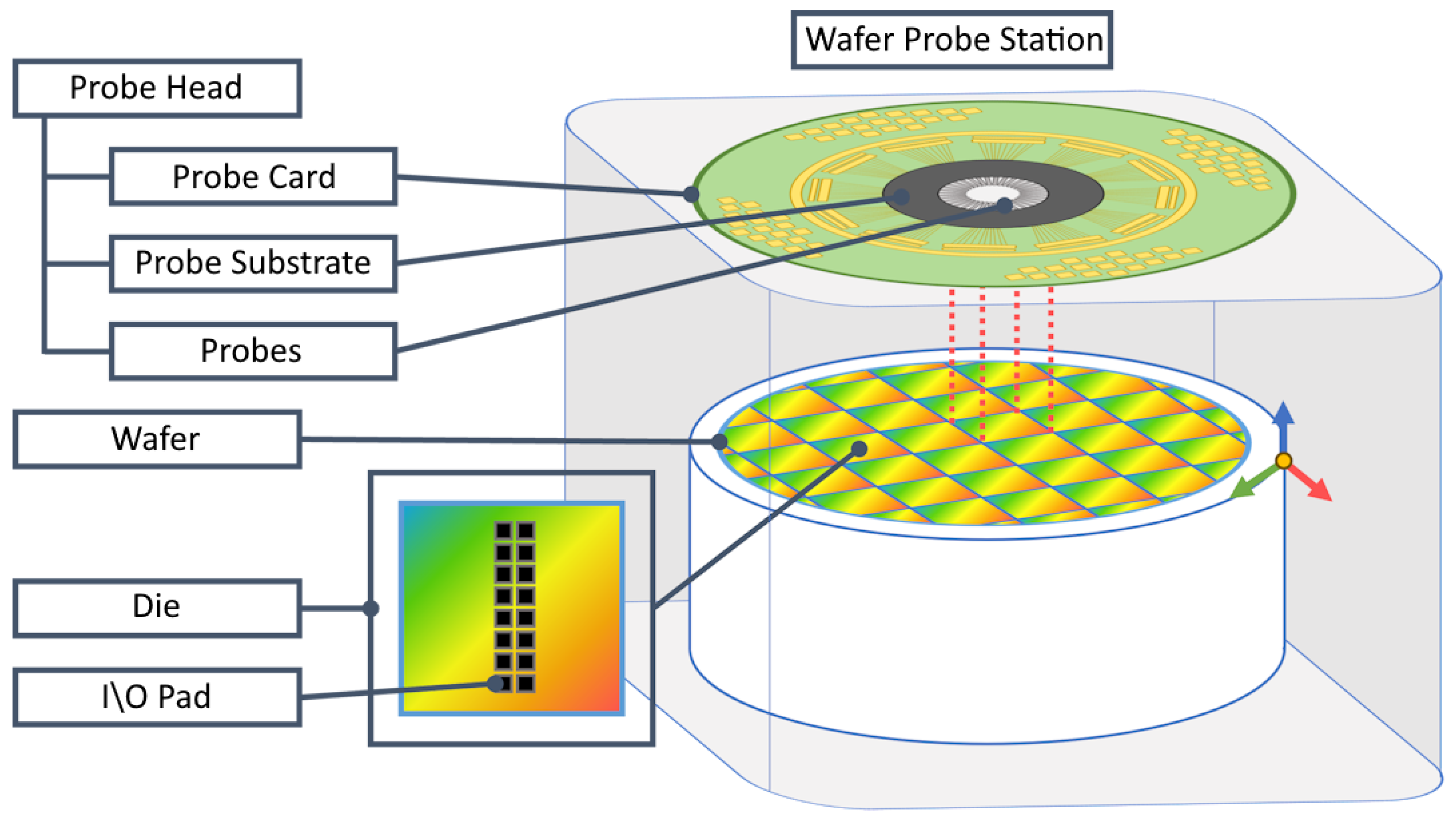
Figure 1. Wafer probe station element composition, with representation of silicon wafer and dies.
Electronics 14 02450 g001
Figure 2. Spring density and available springs at different pitches.
Electronics 14 02450 g002
Figure 3. Pad layout inside a die. From left to right: double strip, cross, double cross, frame, and matrix.
Electronics 14 02450 g003
Figure 4. Three-dimensional representation of a probe head that can make contact with one die per touch.
Electronics 14 02450 g004
Figure 5. Three-dimensional representation of a multi-touch probe head, i.e., one which can make contact with multiple dies with a single touch. It must be noted that the space required to implement this probe head is more than nine times the area required in the probe head showed in Figure 4.
Electronics 14 02450 g005
Figure 6. Layouts of back pads vs. springs.
Electronics 14 02450 g006
Figure 7. Curve representing the cost of a product over time.
Electronics 14 02450 g007
Figure 8. Comparison of the use of different pad layouts in the computation of the front and back area.
Electronics 14 02450 g008
Figure 9. Cost per die at different back pitches.
Electronics 14 02450 g009
Figure 10. Visualization of the components of the graphical user interface, and the flow to follow for using the tool.
Electronics 14 02450 g010
Table 1. Number of dies produced from wafers of different diameters.
Die Side
Length
(mm)
Die AreaDies in 6′′
Wafer
Dies in 8′′
Wafer
Dies in 12′′
Wafer
Dies in 18′′
Wafer
 1 mm  1 mm217,36631,25970,008157,928
 2 mm  4 mm2 4274 772417,366 39,278
 3 mm  9 mm2 1869 3392 7658 17,366
 4 mm 16 mm2 1035 1886 4274  9717
 5 mm 25 mm2  651 1192 2713  6187
 6 mm 36 mm2  445  818 1869  4274
 7 mm 49 mm2  322  594 1362  3123
 8 mm 64 mm2  242  449 1035  2379
 9 mm 81 mm2  188  350  811  1869
10 mm100 mm2  150  280  651  1506
Disclaimer/Publisher’s Note: The statements, opinions and data contained in all publications are solely those of the individual author(s) and contributor(s) and not of MDPI and/or the editor(s). MDPI and/or the editor(s) disclaim responsibility for any injury to people or property resulting from any ideas, methods, instructions or products referred to in the content.