1. Introduction
The output voltage ripple is a critical parameter in the design and performance of DC–DC converters, as it directly influences the required value of the output capacitance connected in parallel with the load. Existing analytical expressions for estimating the ripple, normalized to the average output voltage, have primarily been developed under the assumption of continuous conduction mode (CCM) operation [
1,
2,
3,
4]. However, for boost and buck–boost converters, these expressions require refinement even in CCM when the duty cycle of the transistor’s PWM control signals approaches the boundary between CCM and discontinuous conduction mode (DCM).
In switched-mode DC power supplies where output voltage and load current vary over wide ranges during operation, converters inevitably operate in both CCM and DCM regimes [
5,
6,
7,
8,
9,
10,
11]. Notably, power supplies based on buck–boost topologies—both isolated and non-isolated—are frequently designed to operate in DCM, particularly when controlled via peak current mode without slope compensation, due to the reduced dependence of output voltage on input voltage in this mode [
12,
13,
14,
15,
16,
17]. To optimize performance under such conditions, accurate analytical relations are required for predicting output voltage ripple in DCM.
The output voltage ripple of ideal buck, boost, and buck–boost converters has been examined in references [
18,
19,
20]. In these studies, the derivation of ripple calculation formulas was based on the utilization of equivalent circuit models and an analysis of energy transfer mechanisms.
The various operating modes, which correspond to distinct ripple calculation relationships, have been classified according to the inductance values of the converters. These modes are characterized through graphical representations, thereby complicating the practical application of the methodologies.
In this study, a novel approach is employed to derive the normalized relationships between output voltage ripple and average output voltage for buck, boost, and buck–boost converters. These relationships are obtained by analyzing the waveform of the output capacitor current.
This paper derives such expressions for buck, boost, and buck–boost converters. Additionally, for boost and buck–boost topologies, improved formulas are presented for ripple estimation in CCM operation near the boundary with DCM.
In the proposed approach, the delineation of the applicability domains for the various relationships is performed using an adimensional parameter, as introduced in [
1]. For all converter types, the critical boundary values separating these domains depend solely on the duty cycle of the PWM control signals. This simplification facilitates the calculations and enables a more comprehensive analysis of the impact of the converter component values on the magnitude of the normalized output voltage ripple.
The proposed relationships have been validated through both simulation and experimental testing, demonstrating strong agreement between theoretical predictions and measured results.
2. Peak-To-Peak Voltage Ripple at the Buck Converter Output
Figure 1 illustrates the schematic of a buck converter constructed using a transistor and a diode.
The condition for the operation of the converter in CCM is [
1,
3].
In (1), K represents the dimensionless quantity that defines the conduction mode, L is the converter inductance, f is the switching frequency, R is the load resistance, and D is the duty cycle of the transistor control MID pulses.
When operating in CCM, the relationship for calculating the ripple normalized to the average value of the output voltage of the ideal buck converter is [
1,
3]
In (2), represents the peak-to-peak ripple of the output voltage, is the average value of this voltage, and C is the parallel capacitance of the load resistance.
In the ideal converter, the transistor and diode are considered ideal switches with zero on-resistance, infinite off-resistance, and zero switching times. The other circuit components are considered lossless. The condition for the operation of the buck converter in DCM is [
1,
3]
Figure 2 presents the inductor current
and capacitor current
waveforms corresponding to the ideal buck converter operating in DCM. The waveform
is plotted based on the equation
In this figure, the flyback duty cycle (of the diode) is denoted by , represents the load current assumed as constant (), and is the average value of the inductor current ().
Since the average value of the current through the capacitor is equal to zero, the following relation can be written as
In (5),
represents the peak-to-peak ripple of the inductor current, and
is the switching period. The following relations [
1,
3,
21] are valid for the DCM operating of the buck converter:
where
M is the conversion ratio of the DCM buck converter given by [
1,
21,
22,
23]
From (6) and (7), the following equation results:
The electrical charge
stored in the capacitor for the duration
is given by
Inserting the expression
from (5) into (9), we obtain
In (10),
is replaced with the expression from (8), and the following expression is obtained for the calculation of the peak-to-peak ripple relative to the average value of the output voltage for the DCM operating buck converter:
The following relations are valid at the border between DCM and CCM operating modes:
For a first verification of (11), the relations in (12) are introduced into (11), and the expression (2) is correctly obtained. Over the entire range of variation of the duty cycle
, the peak-to-peak ripple normalized to the average value of the output voltage of the ideal buck converter is expressed by
The procedure for deriving the normalized peak-to-peak ripple of the buck converter’s output voltage, given the input voltage , output voltage , load resistance R, inductance L, and output capacitance C, is outlined as follows:
(a) Assuming the converter operates in CCM, the voltage conversion ratio
M, duty cycle
D, and the dimensionless parameter
K are calculated using the following relations:
Using these computed values, the applicable inequality—either (1) or (3)—is checked to determine whether the converter operates in CCM or in DCM.
(b) If CCM is confirmed, the peak-to-peak ripple of the output voltage is obtained from Equation (2).
(c) If DCM conditions are met, the following steps are performed:
-The duty cycle is calculated with the following relationship derived from (7):
-The ripple of the output voltage is then calculated using (11).
To calculate the normalized peak-to-peak output voltage ripple of the buck converter, given the known parameters input voltage , duty cycle D, load resistance R, inductance L, and output capacitance C, the dimensionless quantity K is computed, and (13) is employed.
The converter output voltage is determined from the value of the conversion ratio M, which in CCM is calculated with (14) and in DCM with (7).
3. Peak-To-Peak Voltage Ripple at the Boost Converter Output
Figure 3 shows the schematic of a boost converter implemented using a transistor and a diode. For an ideal converter operating in continuous conduction mode (CCM), assuming that the output capacitor discharges exclusively during the transistor’s conduction interval (on time), the peak-to-peak voltage ripple, normalized to the average output voltage, is expressed as [
21]
In practice, this relationship is correct only if the following inequality is verified:
Under the condition
the converter will still work in CCM, but the waveforms of the currents through the inductor and through the capacitor are those from
Figure 4. The capacitor will also discharge towards the end of the duration
corresponding to the off interval when the transistor is blocked; therefore, (16) can no longer be used.
The duration
for the capacitor to charge (
) is given by
In the above equation, and represent the average value and the peak-to-peak ripple of the current through the inductor, respectively. denotes the load current, which is assumed to be constant, and is the slope of the current during off time.
The
capacitor current waveform in
Figure 4 is obtained under the condition
For the boost converter working in CCM, the following relations [
1,
3,
21] are valid:
By introducing (21) into (20) and taking into account that the converter operates in CCM, the condition in (18) is obtained.
By introducing (21) in (22), the following expression of the peak-to-peak ripple normalized to the average value of the output voltage of the boost converter is obtained when the inequalities (18) are respected:
The following relation exists for
:
By introducing (24) into (23), the expression for the peak-to-peak ripple normal to the average value of the output voltage from (16) is correctly obtained.
The ratio of
, which is the peak-to-peak ripple of the output voltage deduced from (23), and
, which is the peak-to-peak ripple of the output voltage deduced from Equation (16), is
The maximum of this ratio is obtained for
and corresponds to the boundary between CCM and DCM, and is given as follows:
This ratio evaluates the difference between the normalized ripples given by (16) and (23). From (26), the
Table 1 is obtained.
The result is that if the transition from CCM to MCD is carried out with a duty cycle , then the errors that occur if (23) is not used instead of (16) can become important.
The condition for the operation of the boost converter in DCM is given by [
1,
3,
22]
The waveforms of the currents through the inductor and the capacitor are shown in
Figure 5.
The waveform of the current through the capacitor is plotted based on the following relation:
The duration
for the capacitor to charge (
) is given by
For the boost converter working in DCM, the following relations [
1,
2,
3] are valid:
Equations (30) and (31) lead to the following expression for the peak-to-peak ripple normalized to the average value of the output voltage of the boost converter operating in DCM:
The following relations are valid at the border between the CCM and DCM:
By introducing the relations of K and R from (33) into both (23) and (32), we obtain exactly the same expressions.
Over the entire range of variation of the duty cycle
, the peak-to-peak ripple normalized to the average value of the boost converter output voltage is calculated with the following relation:
The derivation of the normalized peak-to-peak ripple of the boost converter’s output voltage, given the input voltage , output voltage , load resistance R, inductance L, and output capacitance C, is conducted according to the following procedure:
(a) Assuming the converter operates in CCM, the voltage conversion ratio
M, duty cycle
D, and the dimensionless parameter
K are calculated using the following relations:
and the determination of whether the converter operates in CCM or DCM is made by evaluating inequality (27).
(b) If the operation mode occurs in CCM and inequality (17) is satisfied, the normalized peak-to-peak ripple of the output voltage is computed using (16).
(c) If the operation mode is CCM and inequality (18) is verified, the normalized peak-to-peak ripple of the output voltage is calculated with (23).
(d) If the operation mode occurs in DCM, the following additional two steps are necessary:
-The duty cycle is calculated using the following relationship derived from (31):
-The normalized peak-to-peak ripple of the output voltage is calculated using (32).
To calculate the normalized peak-to-peak output voltage ripple of the boost converter, given the known parameters input voltage , duty cycle D, load resistance R, inductance L, and output capacitance C, the dimensionless quantity K is computed, and (34) is employed.
The converter output voltage is determined from the value of the conversion ratio M, which in CCM is 1/(1 − D), and in DCM is given by (31).
4. Peak-To-Peak Voltage Ripple at the Buck–Boost Converter Output
The schematic of the buck–boost converter with a transistor and a diode is shown in
Figure 6. In continuous conduction mode (CCM) operation, the peak-to-peak ripple normalized to the average output voltage is determined using Equation (14), which is similar to the boost converter. For the buck–boost converter, this relationship is valid only if the condition specified in inequality (15) is met. If the inequality is reversed and the converter continues to operate in CCM, the
current waveform follows the pattern shown in
Figure 4. In this case, capacitor discharge also occurs during the off time, rendering Equation (14) invalid.
When operating in CCM, the following relations [
1,
3,
21] apply for the buck–boost converter:
Taking into account (20) and (37) and the operating condition in MCC, for the buck–boost converter, the
waveform from
Figure 4 will be obtained if
Under this condition, the following expression of the peak-to-peak ripple normalized to the average value of the output voltage is obtained from (22) and (37):
If in (39) we consider the particular case
then Equation (16) is correctly obtained.
We denote the peak-to-peak ripple of the output voltage deduced from (39) as
and the peak-to-peak ripple of the output voltage deduced from (16) as
. Their ratio is given by
The maximum of the above ratio is obtained for
and corresponds to the boundary between CCM and DCM, and is given as follows:
The same expression was obtained for the boost converter, so
Table 1 is valid in this case, too. Therefore, if the transition from CCM to DCM is made at a duty cycle
, the errors that occur if (39) is not used instead of (16) can become important.
The condition for the operation of the buck–boost converter in DCM is given by [
2,
23] the following:
When operating in DCM, the waveforms of the currents through the inductor and through the capacitor are shown in
Figure 5, and the following relations [
1,
2,
3] can be written:
The following expression for the peak-to-peak ripple normalized to the average value of the output voltage is obtained from (30) and (44):
For , the expressions in (39) and (45) coincide correctly.
The exact relationship for determining the peak-to-peak ripple normalized to the average value of the output voltage of the ideal buck–boost converter over the entire range of variation of the duty cycle
is the following:
It can be observed that when the buck–boost converter operates in DCM, the peak-to-peak ripple normalized to the average output voltage is independent of the duty cycle and depends solely on the load resistance.
The calculation of the normalized peak-to-peak ripple of the buck–boost converter’s output voltage, given the input voltage , output voltage , load resistance R, inductance L, and output capacitance C, is conducted according to the following procedure:
(a) Assuming the converter operates in CCM, the voltage conversion ratio
M, duty cycle
D, and the dimensionless parameter
K are calculated using the following relations:
The determination of whether the converter operates in CCM or DCM is made by evaluating inequality (43).
(b) If the operation mode occurs in CCM and inequality (38) is not satisfied, the normalized peak-to-peak ripple of the output voltage is computed using (16).
(c) If the operation mode is CCM and inequality (38) is verified, the normalized peak-to-peak ripple of the output voltage is calculated with (39).
(d) If the operation mode occurs in DCM, the normalized peak-to-peak ripple of the output voltage is calculated with (45).
To calculate the normalized peak-to-peak output voltage ripple of the buck–boost converter, given the known parameters input voltage , duty cycle D, load resistance R, inductance L, and output capacitance C, the dimensionless quantity K is first calculated, and then (46) is applied.
The converter output voltage is determined from the value of the conversion ratio M, which in CCM is D/(1 − D), and in DCM is given by (44).
5. Simulation and Experimental Verification of the Novel Expressions for the Peak-to-Peak Ripple Normalized to the Average Value of the Output Voltage
Switching power supplies are usually stabilized. In the simulated and experimentally verified converters, a constant output voltage was chosen. For this, the input voltage was modified accordingly for each converter depending on the duty cycle D. All tested converters have a switching frequency of 100 KHz.
The buck converter parameters were chosen so that at , it would work on the border between CCM and DCM. The other values used for the duty cycle are 0.5, 0.4, and 0.3. The load resistance is (the power dissipated on the load resistance is 100 w), and the load parallel capacitor is .
The characteristic values of the tested buck converter are shown in
Table 2.
Simulations were conducted utilizing the OrCAD Cadence Release 9.2 software, with circuit elements sourced from the PSPICE component libraries.
Table 3 lists the components used as the basis for both the simulation and practical implementation of the three converters: buck, boost, and buck–boost.
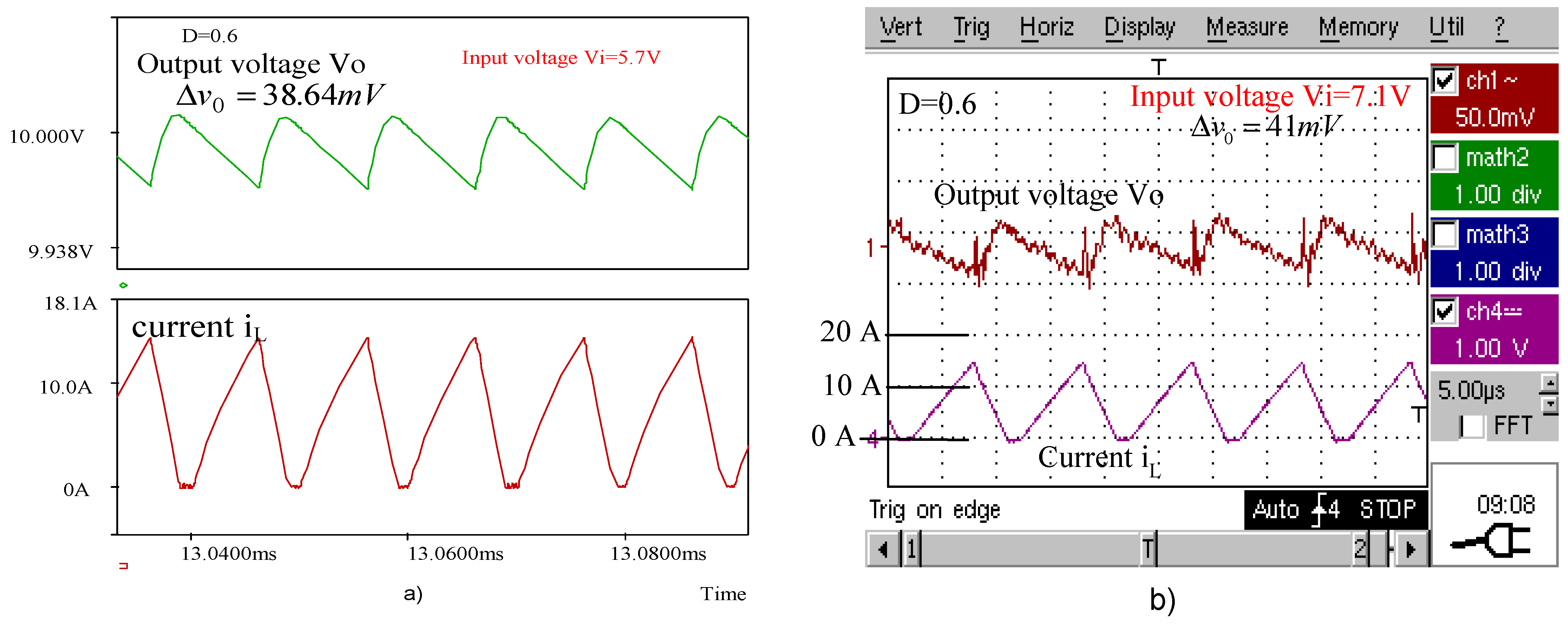
Figure 7a,b present the waveforms of the output voltage
and inductor current
obtained for the buck converter by simulation and by experimental tests, respectively, when operating with a duty cycle
. The same waveforms are given in
Figure 8a,b for
, in
Figure 9a,b for
, and in
Figure 10a,b for
.
The peak-to-peak voltage ripples of the buck converter output are presented in
Table 4. The experimental values are compared with those calculated using the novel expressions and with the simulated ones.
The boost and buck–boost converters that were simulated and experimentally tested had the same characteristic values as the buck converter except that their load resistance was
, corresponding to a power of 20 W, as presented in
Table 5.
Figure 11a,b present the waveforms of the output voltage
and inductor current
obtained for the boost converter by simulation and by experimental tests, respectively, when operating with a duty cycle
. The same waveforms are given in
Figure 12a,b for
, in
Figure 13a,b for
, and in
Figure 14a,b for
.
Table 6 compares the peak-to-peak voltage ripples of the boost converter experimentally obtained with those computed using the novel expressions and with the simulated ones.
Figure 15a,b present the waveforms of the output voltage
and inductor current
obtained for the buck–boost converter by simulation and by experimental tests, respectively, when operating with a duty cycle
. The same waveforms are given in
Figure 16a,b for
, in
Figure 17a,b for
, and in
Figure 18a,b for
.
The peak-to-peak voltage ripples of the buck–boost converter output are presented in
Table 7. The experimental values are compared with those calculated using the novel expressions and with the simulated ones.
6. Conclusions
This paper examines the voltage ripple at the output of DC converters, including the ripple observed during operation in DCM, for which new calculation formulas were derived. For the boost and buck–boost converters, improved formulas are provided to enhance ripple estimation, especially during CCM operation at duty cycles near the transition point between CCM and DCM. This study demonstrates that these new formulas diverge from commonly used ones when the boundary duty cycles are less than or equal to 0.5.
In sources where converters operate in DCM mode, the output voltage depends not only on the duty cycle but also on the load resistance. Consequently, if the sources are regulated and the load resistance varies significantly, the converters will function across a wide range of duty cycles. Therefore, the derived formulas were validated for duty cycle values ranging from 0.3 to 0.6.
The ripple values obtained through calculations and simulations are closely aligned. As anticipated, the values measured in experimental tests are higher, since the derived formulas are based on ideal converter models. Nevertheless, these formulas are still effective for prototype design, with the final output capacitance values being determined through experimental validation.
These novel expressions also provide valuable insights for the design process. First, when a buck converter operates in DCM as opposed to CCM, the inductance value has a minimal impact on the peak-to-peak ripple normalized to the average output voltage. Second, in the case of the buck–boost converter (and consequently the flyback converter), this normalized ripple is independent of the duty cycle.
The derived equations demonstrate that, across all operating modes and for all converters, the normalized ripple relative to the average output voltage is inversely proportional to the value of the output capacitance. These relationships can be employed either to calculate the normalized ripple, given the known component values of the converter, or to determine the required output capacitance to achieve a specified normalized ripple.
Additionally, these relations enable a straightforward assessment of how variations in specific component values—potentially within a broad range—affect the normalized ripple, thereby facilitating optimization efforts.


