Abstract
Compact, broadband, multi-channel RF chips with low loss and high integration are required for high-performance phased-array systems. Presented in this paper is a four-channel, multifunction RF chip operating in the 5–18 GHz frequency range that integrates broadband phase shifting, amplitude control, power amplification, and switching functions. The chip is designed to have flip-chip bonding and stacked gold bumps to enable the compact 3D integration of the GaAs pHEMT and Si-CMOS. To ensure high-density interconnects with minimal parasitic effects, a fan-in redistribution process is implemented. The RF front-end part of this chip, fabricated through a 0.15 µm GaAs pHEMT process, integrates 6-bit digital phase shifters, 6-bit digital attenuators, low-noise amplifiers (LNAs), power amplifiers (PAs), and single-pole double-throw (SPDT) switches. To enhance multi-channel isolation and reduce crosstalk between RF chips and digital circuits, high isolation techniques, including a ground-coupled shield layer in the fan-in process and on-chip shield cavities, are utilized, which achieve isolation levels greater than 41 dB between adjacent RF channels. The measurement results demonstrate a reception gain of 0 dB with ±0.6 dB flatness, an NF below 11 dB, and transmit gain of more than 10 dB, with a VSWR of below 1.6 over the entire 5–18 GHz frequency band. The 6-bit phase shifter achieves a root mean square (RMS) phase error below 2.5° with an amplitude variation of less than 0.8 dB, while the 6-bit attenuator exhibits an RMS attenuation error of below 0.5 dB and a phase variation of less than 7°. The RF and digital chips are heterogeneously integrated using flip-chip and fan-in technology, resulting in a compact chip size of 6.2 × 6.2 × 0.33 mm3. These results validate that this is a compact, high-performance solution for advanced phased-array radar applications.
1. Introduction
The growing demand for broadband, highly integrated, and compact phased-array transceiver chips has driven significant advancements in Monolithic Microwave-Integrated Circuit (MMIC) technology. Phased-array radar operates by electronically steering the beam through precise control of the phase and amplitude of the signal at each antenna element. This technology enables rapid beam scanning and is widely used in advanced applications such as aerospace, detection systems, and next-generation wireless communication systems. In high-performance phased-array radar systems, element spacing plays a critical role in determining system resolution and beamforming accuracy. To achieve optimal performance, particularly at higher frequencies, the spacing between antenna elements is typically required to be less than half the wavelength. This stringent requirement imposes severe constraints on the size of transmit/receive (T/R) modules, necessitating the development of highly integrated, multifunctional RF chips that both optimize electrical performance and have a compact form, as is demonstrated in [1,2].
To address these constraints, RF multifunctional chips have been evolving toward a higher integration density, aiming to achieve precise amplitude and phase control, low noise, and high output power, thereby enabling accurate beamforming in phased-array systems [3]. However, achieving a broadband operation such as 5–18 GHz across multiple transceiver channels within a compact, highly integrated platform remains a significant technical challenge [4]. This frequency range is particularly critical, as it encompasses several key radar and communication bands, enabling a single system to support multifunctional capabilities. Moreover, wideband operation enhances system performance by improving resolution, target discrimination, and spectral efficiency. Further, considerable efforts have been devoted to the development of multifunctional transceiver chips for phased-array systems. Early implementations primarily focused on integrating phase and amplitude control functions to enable basic beamforming capabilities [5,6]. Subsequent advances incorporated low-noise amplifiers and power amplifiers into the same module, thereby enhancing the chip’s reception sensitivity and ability to transmit power [4]. To further increase their spatial resolution and array scalability, several works have explored multi-channel integration, typically of up to two or four RF channels [7,8].
Recently, phased-array transceiver architectures have relied on III-V compound semiconductors, such as GaAs [4,9], GaN [10], and InP [11], due to their superior power handling, low loss, and high-frequency performance. Despite these advantages, such implementations often suffer from large form factors and limited integration capabilities, as additional packaging and interconnects are required to interface them with digital control circuits [12]. In contrast, SiGe BiCMOS- and CMOS [13,14]-based RF solutions have gained traction in recent years, offering lower costs, a higher integration density, and compatibility with digital beamforming architectures. Despite these advantages, CMOS-based RF implementations remain inferior in terms of their noise figure (NF), working frequency, and power handling when compared to their III-V counterparts [15,16]. Table 1 summarizes the key performance parameters of several commonly used semiconductor technologies for RF transceivers, including their frequency range, integration scale, and noise characteristics [16].

Table 1.
Comparison of semiconductor technologies for phased-array transceiver applications.
To overcome these challenges, 3D heterogeneous integration [17,18,19,20] has emerged as a promising solution for achieving compact, high-performance RF front-end designs. By vertically stacking and integrating high-performance GaAs RF circuits with Si-CMOS-based control circuits, this approach enables the realization of miniaturized, multifunctional T/R modules. Beyond front-end integration, heterogeneous integration extends to the back-end and packaging layers. Advanced packaging technologies, such as wafer-level packaging (WLP) and system-in-package (SiP) configurations, facilitate the embedding of passive components—such as resistors, capacitors, and inductors—directly into the packaging substrate. This integration reduces parasitic effects, enhances signal integrity, and contributes to the miniaturization of RF systems. For instance, low-temperature co-fired ceramics (LTCC) technology allows for the incorporation of passive elements within a ceramic substrate, offering improved RF performance and compactness [21]. In the proposed design of the phased-array transceivers, heterogeneous 3D integration effectively combines the high-frequency performance of GaAs with the high-density integration and cost-effectiveness of Si-CMOS, thereby surpassing the limitations of conventional single-process integrated circuits. Further, recent advances in magnetic film engineering and passive component integration—such as Permalloy rings and CoZrTaB thin films—have significantly improved the inductance and quality factors of on-chip RF components [22,23,24]. These techniques support the ongoing movement toward compact, high-frequency multifunctional transceiver designs.
This paper presents a heterogeneously integrated 5–18 GHz four-channel RF multifunction chip, which combines a high-performance GaAs front-end RF with a Si-CMOS digital control circuit. The RF and digital chips are heterogeneously integrated using flip-chip and fan-in technology, resulting in a highly compact chip size of 6.2 × 6.2 × 0.33 mm3. The RF chip, fabricated using a 0.15 μm GaAs pHEMT process, enables four-channel transmission and reception with its 6-bit digital phase shifters, 6-bit digital attenuators, low-noise amplifiers (LNAs), power amplifiers (PAs), single-pole double-throw (SPDT) switches, and power division functions. High-isolation techniques, including a ground-connected shielding layer in the fan-in process and on-chip shielding cavities, are employed to enhance multi-channel isolation and reduce crosstalk, achieving an isolation level exceeding 41 dB between adjacent RF channels. The measurement results show that the maximum amplitude and phase RMS errors are, respectively, less than 0.5 dB and 3.3°. And the multifunction chip achieves a reception gain of 0 dB with ±0.6 dB flatness, an NF of below 11 dB, and transmit gain of more than 10 dB, with a VSWR of below 1.6 over the entire 5–18 GHz frequency band.
The remainder of this paper is structured as follows: Section 2 describes the chip’s architecture and the integration approach used. Section 3 details the RF circuit’s analysis and design, including its amplifiers, phase shifters, and attenuators. Section 4 introduces the high-isolation techniques used to minimize interference. Section 5 presents the measured performance results. A conclusion is given in Section 6.
2. Multifunction Chip Architecture
The proposed multifunctional RF chip employs 3D heterogeneous integration to achieve a compact, high-performance solution for phased-array applications. As shown in Figure 1, the proposed design consists of two primary components. The RF chip is fabricated using a 0.15 μm GaAs pHEMT process; this chip enables a high-performance microwave amplitude and phase control across four channels. The digital chip is implemented using a Si-CMOS process; this chip provides multi-channel serial-to-parallel conversion, power management, electrostatic discharge (ESD) protection, and power-on reset functions. The fan-in process redistributes the I/O contact points of the CMOS chip, allowing seamless integration with the GaAs chip.
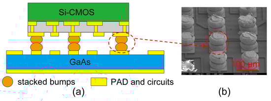
Figure 1.
(a) A block diagram of the designed multifunction chip; it contains an RF circuit realized by the GaAs process and a digital circuit realized by Si-CMOS. Flip chips with stacked gold bumps are utilized for 3D heterogeneous integration. (b) A picture of the stacked bumps which provide mechanical and electrical connections between the RF chip and the digital chip.
The integration of the GaAs RF chip and the Si-CMOS digital chip is realized through 3D heterogeneous stacking. The Si-CMOS chip is flipped and precisely aligned with the GaAs RF chip using a high-precision flip-chip bonder. A stack of gold bumps is utilized for both electrical and mechanical interconnections. Hot pressing and ultrasonic welding are used to create low-resistance electrical interconnects, minimizing contact resistance and interfacial defects. By integrating the GaAs front-end RF and Si-CMOS digital control logic into a single monolithic system, this heterogeneous 3D architecture optimizes the system’s performance, reduces its footprint, and improves its scalability.
As illustrated in Figure 2, the RF circuit is structured with four independent transmission (TX) and reception (RX) channels, each containing a digitally controlled phase shifter, digitally controlled attenuator, low-noise amplifier, power amplifier, and SPDT switches.
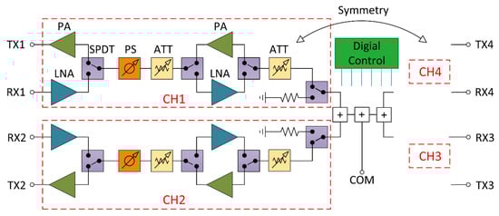
Figure 2.
The four channels of transmission (TX) and reception (RX). The sub-circuits in a single channel contain a power divider, digitally controlled phase shifter (PS), digitally controlled attenuator (ATT), low-noise amplifier (LNA), power amplifier (PA), and single-pole double-throw (SPDT) switch. The circuit topology of channels 3 and 4 is symmetrical to the circuit topology of channels 1 and 2. The digital control part in the Si-CMOS chip enables serial-to-parallel conversion, power-on reset, power-off circuit protection, negative voltage outputs, and other functions.
3. Circuit Design
3.1. Broadband LNA Design for RX Channel
To meet constraints on power efficiency and chip area, a broadband LNA with a cascode structure is adopted in the RX channel, as shown in Figure 3. The LNA employs a common-source (CS) input stage () followed by a common-gate (CG) stage (), providing a favorable trade-off between gain, bandwidth, noise performance, and stability. This structure enables sufficient output swing and low power consumption across the 5–18 GHz frequency band.
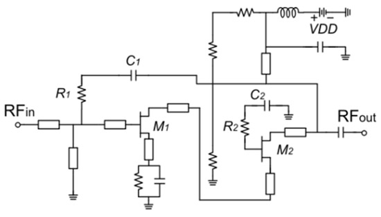
Figure 3.
Schematic diagram of LNA circuit in the reception channel.
The input transistor adopts a CS configuration to achieve high transconductance and a low noise figure. The RC negative feedback circuit, consisting of and , is connected between the source of and the gate of , which enhances input matching, flattens the gain response, and broadens the bandwidth. The CG stage () provides wideband operation and suppresses the Miller effect. A series resistor and a bypass capacitor are added at the gate of M₂ to damp high-frequency oscillations, improving amplifier stability at the expense of a slight reduction in gain.
The voltage gain of the CS–CG cascode amplifier can be approximated as
where is the transconductance of and is the output resistance of . Compared to standalone CS or CG amplifiers, the cascode topology with feedback achieves a superior bandwidth, reverse isolation, and a gain in flatness while maintaining an acceptable noise figure. This design provides a compact, power-efficient solution for wideband phased-array receivers.
3.2. Broadband PA Design for TX Channel
The topology of the power amplifier (PA) for the TX channel is shown in Figure 4. To meet power efficiency requirements, the proposed design adopts a two-stage current-reuse structure, which enhances gain and power efficiency while minimizing overall power consumption. In the first stage, is provided a self-biased circuit for the required gate bias voltage, ensuring its stable operation across varying process and temperature conditions. During the second stage, is powered through a positive power supply voltage divider, which sets the gate and drain voltages for optimal performance. The source voltage of is used to bias the drain of , enabling efficient current reuse and reducing circuit power consumption. In the circuit design phase, appropriate loss and negative feedback are introduced to maintain sufficient amplifier gain and while ensuring absolute stability over the 5–18 GHz frequency range.
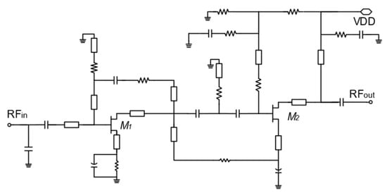
Figure 4.
Schematic diagram of PA circuit in the transmitter channel.
3.3. Design of High-Precision Broadband Phase Shifter
The 6-bit digitally controlled phase shifter consists of six phase shift units positioned at 5.625°, 11.25°, 22.5°, 45°, 90°, and 180°, enabling a full phase shift range of 0 to 354.375° with a step of 5.625°. As shown in Figure 5, the 45°, 90°, and 180 ° phase shift units use a switch-selected all-pass network, which provides higher phase shift accuracy, improved impedance matching, and mutual compensation in terms of transmission loss and additional amplitude-modulation slope. The 5.625°, 11.25°, and 22.5° phase shift units also employ an all-pass network topology to ensure broadband performance and phase stability.
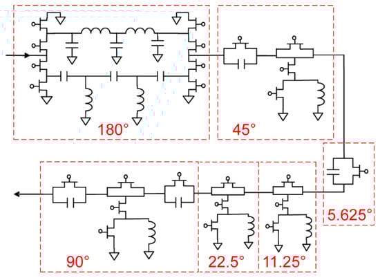
Figure 5.
The schematic of the cascaded 6-bit digital phase shifter.
To enhance stability and minimize mismatch effects, the smaller phase shift units (5.625°, 11.25°, and 22.5°), which are more sensitive to impedance mismatches, are positioned in the middle of the cascaded phase shifter network. Meanwhile, the larger phase shift units (45°, 90°, and 180°), which exhibit a stronger mismatch tolerance, are placed at both ends of the cascaded structure.
The measured results for all 64 states of the phase shift are shown in Figure 6, which shows that the phase shift in the four channels covers 0 to 354.375° with a step of 5.625°. Phase shift accuracy is a critical parameter in the phased array, as it directly impacts beamforming precision. The measured root mean square (RMS) phase errors of the four channels are shown in Figure 7, which shows that the RMS phase error is lower than 2.5° over the frequency from 5 GHz to 16.5 GHz and lower than 3° at 16.5–18 GHz. Figure 8 shows the measured results of the amplitude variations caused by phase shifting, which shows that the corresponding amplitude variations are within ±0.8 dB at the frequency band of 5–16 GHz, and within ±1.5 dB from 16 to 18 GHz. The performance of the phase shifter degrades at 16–18 GHz. The increased RMS phase error and amplitude variation here are mainly due to the limited bandwidth of the phase shifter and the impedance mismatch caused by the subsequent circuits, which becomes more significant near the high-frequency end of the bandwidth.
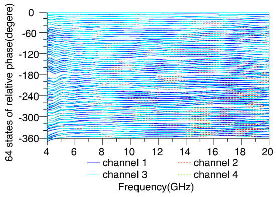
Figure 6.
Measured results of 64 states of phase shifting.
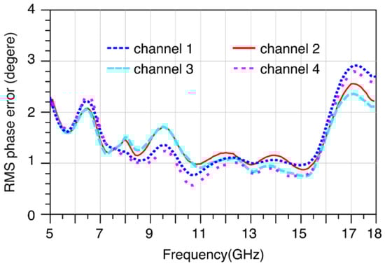
Figure 7.
RMS phase error of a four-channel phase shifter over 5–18 GHz. The plot shows the root mean square (RMS) amplitude error versus frequency for each of the four channels.
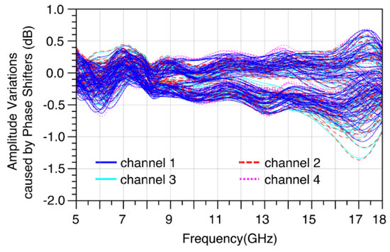
Figure 8.
The amplitude variations caused by 64 states of phase shifting.
These results validate the high precision, broadband performance, and phase stability of the proposed digitally controlled phase shifter, making it well suited for a multifunction chip in a phased-array system.
3.4. Design of High-Precision Broadband Attenuator
The 6-bit digital controlled attenuator utilizes six attenuation units of 0.5 dB, 1 dB, 2 dB, 4 dB, 8 dB, and 16 dB, enabling an attenuation range of 0 to 31.5 dB with a step size of 0.5 dB. As shown in Figure 9, different attenuator architectures are utilized in the proposed design, including switched-T, switched-Π, and switched-path networks.
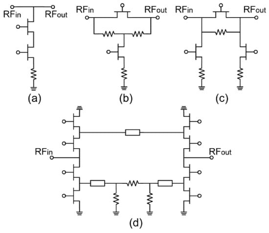
Figure 9.
Different attenuator architectures used in the proposed design. (a) Simplified switched-T structure for 0.5 dB and 1 dB attenuation. (b) Switched-T structure for 2 dB attenuation. (c) Switched-Π structure for 4 dB and 8 dB attenuation. (d) Switched-path structure for 16 dB attenuation.
The 0.5 dB and 1 dB attenuators are particularly sensitive to small series resistance variations in the switched-T structure but have a smaller impact on the input and output voltage standing wave ratios (VSWRs). To mitigate resistance-related losses, a simplified switched-T attenuation cell, as shown in Figure 9a, is employed for these small attenuation levels.
The 2 dB attenuator uses the switched-T network shown in Figure 9b. The 4 dB and 8 dB attenuators use the switched-Π network shown in Figure 9c. In the switched-Π network, attenuation is achieved by controlling series and parallel switches. When the series switch is ON and the parallel switch is OFF, the circuit enters an attenuation state. When the series switch is OFF and the parallel switch is ON, the circuit enters a reference state, minimizing insertion loss.
The 16 dB attenuator employs the switched-path network shown in Figure 9d. In this configuration, SPDT switches are utilized for the selection of either the reference patch or attenuation path. The reference path consists of a microstrip delay line, and the attenuation path is a Π-type attenuation impedance network. The microstrip delay line compensates for parasitic phase shift in the attenuation path, ensuring minimal additional phase shift between the two paths.
The measured attenuation characteristics across all 64 states are shown in Figure 10, which shows that the attenuation of the four channels covers 0 to 31.5 dB with a step of 0.5 dB. To evaluate the attenuation accuracy, the RMS attenuation error is calculated from the measurement results, as shown in Figure 11. This shows that the RMS attenuation error remains below 0.5 dB across the 5–18 GHz frequency range, demonstrating high precision. The phase variation caused by the attenuation states is presented in Figure 12, which shows that the phase variations are within ±8° across the entire 5–18 GHz band.
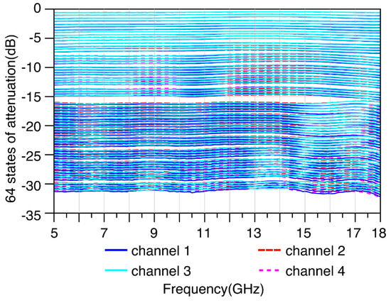
Figure 10.
Measured results for the 64 states of attenuation.
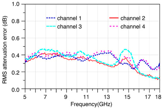
Figure 11.
RMS attenuation error of a four-channel phase shifter over 5–18 GHz.
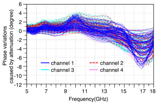
Figure 12.
Additional phase variation caused by the 64 attenuation states.
4. High-Isolation Design
High-performance phased-array systems require compact, broadband, and multi-channel RF chips. The increasing demand for such devices has driven significant advancements in the integration of RF multifunctional chips. As a result, chip dimensions continue to shrink, making high isolation between different channels and isolation between adjacent functional circuits increasingly important.
To achieve seamless integration, a flip-chip bonding and fan-in process is employed to connect the GaAs-based RF chip with the Si-CMOS digital control chip, as shown in Figure 1b. A flow diagram of the heterogeneous 3D integration process, including fan-in redistribution, gold bumping, and flip-chip bonding is provided in Figure 13. Stacked gold bumps with a diameter of 55 μm are vertically planted on the chip pads, ensuring both mechanical support and reliable electrical interconnection. The vertical distance between the GaAs and Si-CMOS chips is approximately 50 μm, which necessitates the careful use of interference mitigation strategies to minimize unwanted coupling between the digital and RF circuits.
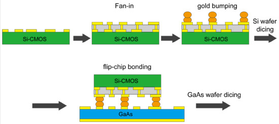
Figure 13.
A process flow diagram of the heterogeneous 3D integration process.
4.1. Challenges in Achieving High Isolation Between RF and Digital Chips
The flip-chip bonding process of the Si-CMOS chip is employed in heterogeneous 3D integration to enable its high electrical performance by providing a shorter interconnect path between the digital control chip and the RF multifunctional chip. However, heterogeneous 3D integration creates a complex electromagnetic environment, where multiple signals—microwave signals, digital control signals, and power supply noise—coexist. When Si-CMOS chips are flipped and mounted on the GaAs chips, it will inevitably alter the electromagnetic field environment of the active GaAs devices, thereby affecting the parasitic parameters of the active devices and signal transmission.
The original microstrip line transmission mode on the GaAs surface will change to a non-uniform suspended stripline mode. At this time, the impedance of the original matching point will change, resulting in circuit mismatch and a generally larger transmission loss. Further, in the proposed design, an additional metal shielding layer connected to the ground is introduced during the fan-in process. This shielding layer isolates the digital signal on the Si-CMOS chip from the RF signal on the GaAs chip while satisfying the pressure point interconnection between the Si chip and the GaAs chip, thereby achieving a design with good electromagnetic compatibility.
4.2. Design for High Isolation Between RF and Digital Chips
The proposed four-channel RF chip has a compact footprint of 6.2 × 6.2 mm2 (0.2 × 0.2 λ2 at 10 GHz). Due to its high integration density, the mutual coupling effects between different channels and between various functional circuits are significant. These coupling effects will interfere with the RF signal’s integrity and the DC voltage’s stability. The integrated design of the Si and GaAs chips is required to suppress crosstalk and preserve RF performance.
In the proposed design, shielding cavities are introduced to improve the isolation between different channels and between various functional circuits. Figure 14a shows a diagram of the traditional four-channel multifunction chip, while Figure 14b presents the proposed four-channel multifunction chip, which incorporates shielding cavities. Figure 14c depicts an individual channel, where sub-circuits are denoted by orange boxes and shielding cavities are outlined with red dashed lines. These shielding cavities are constructed using stacked bumps interconnected by microstrip lines and ground layers within the RF and digital chips, effectively reducing electromagnetic coupling.
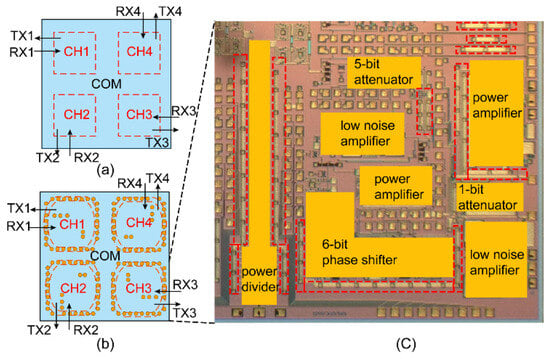
Figure 14.
The shielding cavity constructed in the proposed design to improve isolation. (a) A diagram of the traditional four-channel multifunction chip. (b) A diagram of the proposed four-channel multifunction chip with shielding cavities. (c) A picture of a single channel in the RF chip. The red dashed lines depict the shielding cavities formed by stacked bumps, which are connected by microstrip lines and the ground layer in the RF and digital chips.
To characterize the isolation enhancement of the shielding cavities, the effect of two parallel microstrip lines with a gap of 235 μm was calculated using electromagnetic simulation software. The simulated coupling coefficient, with and without the shielding cavities, is shown in Figure 15a, where the blue dashed line represents the case without shielding cavities and the red solid line represents the case with shielding cavities. It can be seen that the isolation has been improved by about 16 dB. Further, the measured coupling coefficient between two adjacent RF channels on the multifunction chip is shown in Figure 15b, which demonstrates that the isolation exceeds 41 dB, confirming the effectiveness of the proposed shielding cavity design in mitigating inter-channel interference.
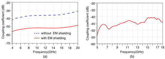
Figure 15.
(a) The simulation results of the coupling coefficient between channels with and without shielding. (b) The measured results of the coupling coefficient between two adjacent RF channels.
The improvement in isolation not only improves channel-to-channel isolation but also effectively separates functional sub-circuits within individual channels, thereby enhancing overall chip performance. This technical route solves the electromagnetic interference problem between adjacent channels and adjacent sub-circuits, ensures the integrity of RF signals within each sub-circuit, and effectively weakens the mutual coupling between sub-circuits and channels. From a fabrication perspective, the implementation of shielding cavities poses several challenges. These include the need for high bump uniformity, precise alignment between the RF and digital dies during the flip-chip bonding process, and careful impedance control to minimize any undesired signal reflections. Nonetheless, the proposed structure enables effective electromagnetic isolation within a compact heterogeneous 3D integration framework, without increasing the overall footprint of the chip.
5. Measurement Results
The designed four-channel multifunction chip was fabricated through a 0.15 μm GaAs pHEMT process. A picture of the heterogeneous integrated chip is shown in Figure 16, with the RF chip being 6.2 × 6.2 mm2. The profile height of the heterogeneous integrated chip is 0.33 mm. The measured results of 64 states of phase shifting are given in Figure 6, Figure 7 and Figure 8. And the measured results of 64 states of attenuation are given in Figure 10, Figure 11 and Figure 12. In summary, the RMS error of the phase shift is less than 3°, and the parasitic amplitude variation in the phase shifter is less than 0.8 dB. The RMS error of the attenuation is less than 0.5 dB, and the corresponding phase variations are within ±8°. The measurement results for the transmission and reception channels are shown in Figure 17, Figure 18 and Figure 19. All measurement results are consistent with the design’s goals.
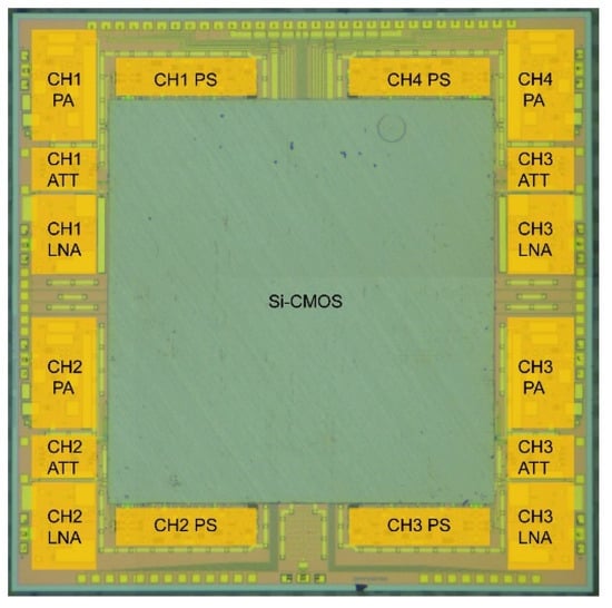
Figure 16.
A photograph of the four-channel multifunctional RF chip heterogeneously integrated with a Si-CMOS chip.
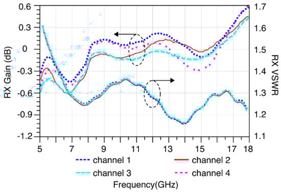
Figure 17.
The measured small-signal gain and VSWR of the reception channel.
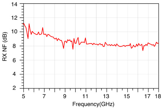
Figure 18.
The measured NF of the reception channel.
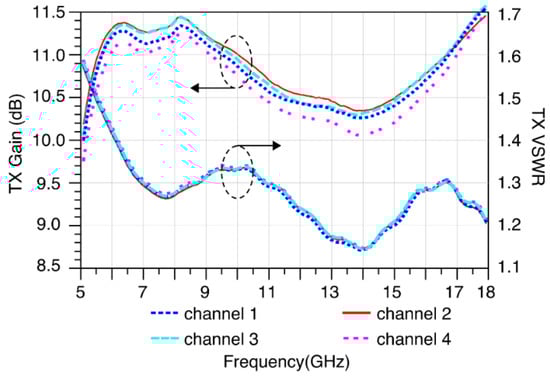
Figure 19.
The measured small-signal gain and VSWR of the transmission channel.
Figure 17 depicts the measured small-signal gain and VSWR of the four reception channels. It can be observed that the typical value of the receiving gains is greater than 0 dB with a good gain flatness of ±0.6 dB. The VSWR of the reception channels are lower than 1.6. Figure 18 depicts the measured noise figure (NF) of one reception channel, which shows that the NF is lower than 11 dB in the working frequency band. The reception channel exhibits a NF below 11 dB, which is relatively high for sensitive applications such as radar or communication systems, where a lower NF is often desired. It is important to clarify that in practical phased-array radar and communication systems, the proposed multifunctional RF chip would not typically be deployed as the first stage of the front-end receiver. Instead, it is preceded by an external LNA and limiter, which provide front-end protection and establish the dominant contribution to the overall system’s noise figure. Hence, the noise contribution of the multifunctional chip is significantly suppressed across the whole receiving chain according to the formula used for the cascaded noise figure.
Figure 19 depicts the measured small-signal gains and VSWR of the transmission channels. It can be seen that in their transmitting state, the typical value of the transmission gain is greater than 10 dB, with a VSWR lower than 1.6. Figure 20 depicts the measured output power of the transmission channel under different ambient temperatures. The proposed chip demonstrates a 1 dB compression point (P1dB) exceeding 19 dBm at 25 °C, with the output power remaining above 20 dBm at –55 °C and above 18 dBm at 85 °C. These results confirm that the transmitter maintains a stable performance and linearity across a wide temperature range, demonstrating a robustness suitable for various environmental conditions.
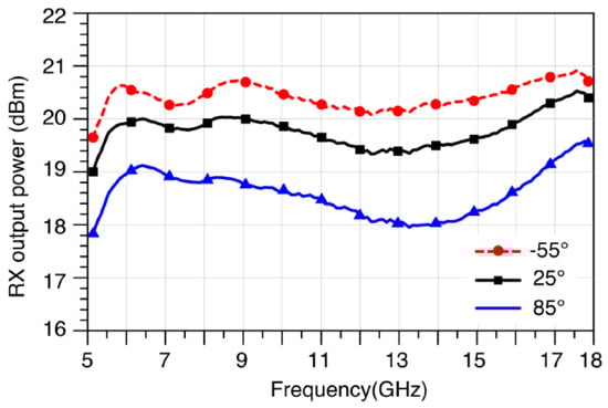
Figure 20.
The measured output power of the transmission channel at different environmental temperatures.
To further demonstrate the advantages of the proposed design, Table 2 presents its comparison with representative state-of-the-art multifunctional transceiver chips. Key parameters such as process technology, operating frequency range, the resolution of the phase shifter and attenuator, RMS phase and amplitude errors, the number of integrated channels, digital chip integration capability, and chip area are evaluated. As shown, some existing works either focus on narrowband implementations, offer fewer channels, or lack digital control integration. In contrast, the proposed chip achieves four-channel operation across a wide frequency band (5–18 GHz), with 6-bit resolution in both its phase and amplitude control, and achieves competitive accuracy (RMS phase error <3°, RMS attenuation error <0.5 dB) while incorporating a Si-CMOS digital control chip into its system through heterogeneous 3D integration. This integration significantly enhances the system’s compactness and scalability.
Table 2.
Performance comparison of relevant multifunction chips.
6. Conclusions
This paper presents a 5–18 GHz four-channel multifunctional RF chip based on the heterogeneous 3D integration of GaAs and Si-CMOS technologies. The proposed chip can handle broadband phase shifting, amplitude control, power amplification, and switching functions within a compact footprint of 6.2 × 6.2 × 0.33 mm3, making it well suited to advanced phased-array radar systems.
To address the challenges with high integration, this work employs flip-chip bonding and stacked gold bumps, enabling a compact 3D integration of the RF and digital chips. A fan-in redistribution process is implemented to ensure high-density interconnections with minimal parasitic effects. To further improve multi-channel isolation, a shielding layer is added in the fan-in redistribution process, reducing the interference between the RF and digital circuits. At the same time, on-chip shielding cavities significantly improve the isolation between adjacent channels and adjacent sub-circuits.
The measured results of the chip’s performance are consistent with the design targets. Within a working frequency band of 5–18 GHz, the receiving gains are greater than 0 dB with a good gain flatness of ±0.6 dB and a NF lower than 11 dB. The VSWR of the reception channels is lower than 1.6. The small-signal gains of the transmission channels are greater than 10 dB with a VSWR lower than 1.6. The 64-state phase shift root mean square (RMS) error is less than 3°, and the additional amplitude variation in the phase shifter is less than 0.8 dB; the 64-state attenuation RMS error is less than 0.5 dB, and the parasitic amplitude modulation RMS is less than 7°. The isolation between the RF channels is above 41 dB. These results validate the feasibility and effectiveness of the proposed heterogeneous 3D integration approach to creating compact, high-performance phased-array transceivers.
Author Contributions
Methodology, B.D.; Validation, B.D.; Investigation, B.D.; Writing—original draft, B.D.; Writing—review & editing, Z.W.; Supervision, Z.W.; Project administration, F.Y. All authors have read and agreed to the published version of the manuscript.
Funding
This research received no external funding.
Data Availability Statement
The original contributions presented in this study are included in the article. Further inquiries can be directed to the corresponding author.
Conflicts of Interest
The authors declare no conflict of interest.
References
- Kim, H.T.; Park, B.S.; Song, S.S.; Moon, T.S.; Kim, S.H.; Kim, J.M.; Chang, J.-Y.; Ho, Y.C. A 28-GHz CMOS Direct Conversion Transceiver with Packaged 2 × 4 Antenna Array for 5G Cellular System. IEEE J. Solid-State Circuits 2018, 53, 1245–1259. [Google Scholar] [CrossRef]
- Zhou, P.; Chen, J.; Yan, P.; Yu, J.; Hu, J.; Dong, H.; Wang, L.; Hou, D.; Gao, H.; Hong, W. A −28.5-dB EVM 64-QAM 45-GHz Transceiver for IEEE 802.11aj. IEEE J. Solid-state Circuits 2021, 56, 3077–3093. [Google Scholar] [CrossRef]
- Ramella, C.; Longhi, P.E.; Pace, L.; Nasri, A.; Ciccognani, W.; Pirola, M.; Limiti, E. Ultralow-Power Digital Control and Signal Conditioning in GaAs MMIC Core Chip for X-Band AESA Systems. IEEE Trans. Microw. Theory Tech. 2022, 70, 367–379. [Google Scholar] [CrossRef]
- Jeong, J.-C.; Yom, I.-B.; Kim, J.-D.; Lee, W.-Y.; Lee, C.-H. A 6–18-GHz GaAs Multifunction Chip with 8-bit True Time Delay and 7-bit Amplitude Control. IEEE Trans. Microw. Theory Tech. 2018, 66, 2220–2230. [Google Scholar] [CrossRef]
- Liang, Q.; Wang, K.; Wang, X.; Yan, Y.; Liang, X. An S–K Band 6-Bit Digital Step Attenuator with Ultra Low Insertion Loss and RMS Amplitude Error in 0.25 μm GaAs p-HEMT Technology. Appl. Sci. 2024, 14, 3887. [Google Scholar] [CrossRef]
- Zhang, L.; Zhao, C.; Zhang, X.; Wu, Y.; Kang, K. A CMOS K-Band 6-bit Attenuator with Low Phase Imbalance for Phased Array Application. IEEE Access 2017, 5, 19657–19661. [Google Scholar] [CrossRef]
- Zhou, S.; Zhou, S.; Zhang, J.; Wu, J.; Yang, H.; Wang, Z. A 7.5–9 GHz GaAs Two-Channel Multi-Function Chip. Electronics 2019, 8, 395. [Google Scholar] [CrossRef]
- Lu, X.; Zhou, S.; Wei, B.; Zhou, L. Three-Dimensional SIP Design of the Four-Channel RF Transceiver Based on Silicon and ALN for X-Band Radar Applications. IEEE Trans. Components, Packag. Manuf. Technol. 2023, 13, 1030–1044. [Google Scholar] [CrossRef]
- Yuan, Y.; Zeng, J.; Zhang, D.; Li, J.; He, D.; Tan, C.; Yu, Z. An X-Band High-Accuracy GaAs Multifunction Chip with Amplitude and Phase Control. IEEE Access 2023, 11, 3872–3880. [Google Scholar] [CrossRef]
- Chiu, H.-C.; Chen, C.-M.; Chang, L.-C.; Kao, H.-L. A 5-Bit X-Band GaN HEMT-Based Phase Shifter. Electronics 2021, 10, 658. [Google Scholar] [CrossRef]
- Kim, S.-K.; Maurer, R.; Simsek, A.; Urteaga, M.; Rodwell, M.J.W. An Ultra-Low-Power Dual-Polarization Transceiver Front-End for 94-GHz Phased Arrays in 130-nm InP HBT. IEEE J. Solid-state Circuits 2017, 52, 2267–2276. [Google Scholar] [CrossRef]
- Gu, X.; Liu, D.; Sadhu, B. Packaging and Antenna Integration for Silicon-Based Millimeter-Wave Phased Arrays: 5G and Beyond. IEEE J. Microwaves 2021, 1, 123–134. [Google Scholar] [CrossRef]
- Carosi, D.; Bettidi, A.; Nanni, A.; Marescialli, L.; Cetronio, A. A Mixed-Signal X-Band SiGe Multi-Function Control MMIC for Phased Array Radar Applications. In Proceedings of the 2009 European Microwave Conference (EuMC), Rome, Italy, 29 September 2009–1 October 2009; pp. 240–243. [Google Scholar]
- Jeong, J.; Yom, I. X-band high power SiGe BiCMOS multi-function chip for active phased array radars. Electron. Lett. 2011, 47, 618–619. [Google Scholar] [CrossRef]
- Razavi, B.; Behzad, R. RF Microelectronics; Prentice Hall: New York, NY, USA, 2012. [Google Scholar]
- Du Preez, J.; Sinha, S.; Sengupta, K. SiGe and CMOS Technology for State-of-the-Art Millimeter-Wave Transceivers. IEEE Access 2023, 11, 55596–55617. [Google Scholar] [CrossRef]
- Roozeboom, F.; Kemmeren, A.; Verhoeven, J.; Heuvel, F.V.D.; Klootwijk, J.; Kretschman, H.; Frič, T.; van Grunsven, E.; Bardy, S.; Bunel, C.; et al. Passive and heterogeneous integration towards a Si-based System-in-Package concept. Thin Solid Films 2006, 504, 391–396. [Google Scholar] [CrossRef]
- Xiang, C.; Jin, W.; Huang, D.; Tran, M.A.; Guo, J.; Wan, Y.; Xie, W.; Kurczveil, G.; Netherton, A.M.; Liang, D.; et al. High-Performance Silicon Photonics Using Heterogeneous Integration. IEEE J. Sel. Top. Quantum Electron. 2022, 28, 15. [Google Scholar] [CrossRef]
- Hagelauer, A.; Wojnowski, M.; Pressel, K.; Weigel, R.; Kissinger, D. Integrated Systems-in-Package. IEEE Microw. Mag. 2018, 19, 48–56. [Google Scholar] [CrossRef]
- Yang, X.; Huang, Y.-S.; Zhou, L.; Zhao, Z.; Ni, D.-X.; Zhang, C.-R.; Mao, J.-F.; Han, J.-A.; Cheng, X.; Deng, X.-J. Low-Loss Heterogeneous Integrations with High Output Power Radar Applications at W-Band. IEEE J. Solid-State Circuits 2022, 57, 1563–1577. [Google Scholar] [CrossRef]
- Heyen, J.; von Kerssenbrock, T.; Chernyakov, A.; Heide, P.; Jacob, A. Novel LTCC/BGA modules for highly integrated millimeter-wave transceivers. IEEE Trans. Microw. Theory Tech. 2003, 51, 2589–2596. [Google Scholar] [CrossRef]
- Xu, W.; Sinha, S.; Dastagir, T.; Wu, H.; Bakkaloglu, B.; Gardner, D.S.; Cao, Y.; Yu, H. Performance Enhancement of On-Chip Inductors with Permalloy Magnetic Rings. IEEE Electron Device Lett. 2011, 32, 69–71. [Google Scholar] [CrossRef]
- Wu, H.; Gardner, D.S.; Xu, W.; Yu, H. Integrated RF On-Chip Inductors with Patterned Co-Zr-Ta-B Films. IEEE Trans. Magn. 2012, 48, 4123–4126. [Google Scholar] [CrossRef]
- Wu, Y.; Yeng, I.-C.; Yu, H. The improvement of CoZrTaB thin films on different substrates for flexible device applications. AIP Adv. 2021, 11, 025139. [Google Scholar] [CrossRef]
- Sim, S.; Jeon, L.; Kim, J.G. A Compact X-Band Bi-Directional Phased-Array T/R Chipset in 0.13 μm CMOS Technology. IEEE Trans. Microw. Theory Tech. 2013, 61, 562–569. [Google Scholar] [CrossRef]
- He, D.; Yu, Z.; Chen, J.; Du, K.; Zhu, Z.; Cheng, P.; Tan, C. A 10-20 GHz 6-Bit High-Accuracy Digital Step Attenuator with Low Insertion Loss in 0.15 μm GaAs p-HEMT Technology. Micromachines 2024, 15, 84. [Google Scholar] [CrossRef]
Disclaimer/Publisher’s Note: The statements, opinions and data contained in all publications are solely those of the individual author(s) and contributor(s) and not of MDPI and/or the editor(s). MDPI and/or the editor(s) disclaim responsibility for any injury to people or property resulting from any ideas, methods, instructions or products referred to in the content. |
© 2025 by the authors. Licensee MDPI, Basel, Switzerland. This article is an open access article distributed under the terms and conditions of the Creative Commons Attribution (CC BY) license (https://creativecommons.org/licenses/by/4.0/).