Abstract
In this article, we present a triple-band Doherty power amplifier (DPA) with a Schiffman phase shifter, which achieved a 90-degree phase shift to facilitate broad frequency range operations. As the cornerstone of the triple-band DPA, the Schiffman phase shifter enabled simultaneous triple-band operations. Furthermore, the entire triple-band Doherty amplifier was designed and fabricated using GaN on SiC HEMT devices, confirming its practical applicability and robust performance. It achieved an output power of 34 dBm at the low-band (LB) frequency of 0.8 GHz, accompanied by a peak drain efficiency (DE) of 53%. Similarly, at the mid-band (MB) frequency of 1.6 GHz, the amplifier maintained an output power of 32 dBm with an identical peak DE of 45%. At the high-band (HB) frequency of 2.2 GHz, the DPA continued to deliver an output power of 33 dBm, again with a peak DE of 50%.
1. Introduction
The accelerated evolution of wireless communication systems has culminated in the standardization of fourth- and fifth-generation (4G and 5G) technologies. These advancements necessitate the development of power amplifiers capable of efficient operation across an extensive range of frequency bands to accommodate the diverse requirements of modern communication protocols. This paper delves into the design and implementation of a sophisticated triple-band Doherty power amplifier (DPA), which leverages the capabilities of a Schiffman phase shifter. This phase shifter is critical in achieving a precise 90-degree phase shift, ensuring optimal performance over a broad frequency spectrum and enhancing the DPA’s efficiency.
Modern mobile systems use multiple band-specific amplifiers, which increase costs and occupy space. A single multi-band amplifier could lower expenses and conserve space, improving the overall device efficiency and compactness. The advantages of this investigation include using a single amplifier instead of multiple ones for different bands, reducing power consumption and costs. Hence, it will serve as a strong foundation for future wideband research.
Previous research and development efforts have primarily focused on optimizing DPAs for dual-band operations [1,2,3,4,5], addressing the immediate needs of specific communication standards. However, the increasing complexity and evolving demands of contemporary wireless systems have driven the shift towards tri-band [6] and broad-band configurations [7,8,9,10]. These configurations aim to provide more versatile and efficient amplifier solutions that are capable of meeting stringent performance requirements across multiple frequency bands.
To address this issue, this paper presents a triple-band Doherty power amplifier (DPA) topology. This proposed design employs a Schiffman phase shifter to achieve precise phase alignment across three frequency bands. By integrating this advanced phase shifter, the proposed DPA topology effectively supports multiple bands, thereby reducing the need for separate power amplifiers for each band. This solution not only minimizes the physical footprint and costs associated with multiple amplifiers but also enhances the efficiency and performance of mobile communication systems.
2. An Analysis of the Proposed Doherty Power Amplifier
2.1. Conventional Doherty Power Amplifier
Figure 1 shows the conventional DPA, consisting of a carrier amplifier (class AB) for efficient low-power amplification and a peaking amplifier for handling peak power levels. The carrier amplifier balances linearity and efficiency by conducting for more than half but for less than the full input cycle. The peaking amplifier operates in class C mode, activating during high power demands to improve efficiency. Though less linear, it provides additional power during signal peaks, maintaining the overall amplifier efficiency.
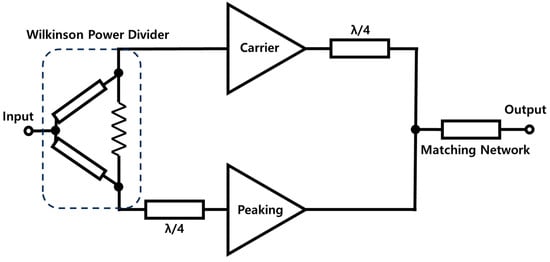
Figure 1.
Conventional Doherty power amplifier.
Additionally, a Wilkinson power divider is employed as the input power splitter, ensuring an even distribution of the input signal between the carrier and peaking amplifiers. This ensures that the signal is evenly distributed, maintaining the phase and amplitude balance required for optimal performance. The outputs of the carrier and peaking amplifiers are combined in a way that optimizes efficiency. This network ensures that the contributions of both amplifiers are effectively merged to produce the desired output power, thereby optimizing the DPA’s performance by effectively managing power across varying operational conditions.
2.2. Schiffman Phase Shifter
The 90-degree Schiffman phase shifter is a specific type of microwave phase shifter designed to provide a constant phase shift of 90 degrees over a broad frequency range. It was first introduced by B.M. Schiffman in 1958 [11] and is particularly valued for its compact size, simplicity, and versatile performance [12,13]. This Schiffman phase shifter consists of a parallel coupled-line section with a connected end as the main line and a uniform transmission line as the reference line. The coupled-line section is characterized by even-mode impedance () and odd-mode impedance (). The uniform transmission line is expressed as 3λ/4. In the context of coupled lines, the even capacitance is configured between the ground and the coupled lines, while the odd capacitance is positioned between the coupled lines and can be calculated using the following method:
A phase shift () in a Schiffman phase shifter is achieved as the phase difference between a uniform transmission line and a coupled section. Kθ denotes the transmission phase of uniform transmission lines [14].
The Schiffman phase shifter was extensively analyzed using various configurations of parallel-connected coupled lines to explore their combined utilization.
Figure 2 illustrates the calculations employed in the proposed triple-band Doherty power amplifier (DPA). When = and K = 3, the calculations can be derived from Equations (2) and (3). Our goal was to achieve triple-band coverage encompassing the major frequency bands used in LTE, NR 5G, WCDMA, and GSM cellular communications. We focused on a center frequency of 1.8 GHz within the 1710–1980 MHz range of the mid-band frequencies. This choice allowed us to reach both low and high bands with the help of a Schiffman phase shifter. To achieve this, we used = 200 Ω, = 50 Ω, and a center frequency of 1.8 GHz with a quarter-wavelength (λ/4) coupled line. This approach helped us meet our goal effectively.
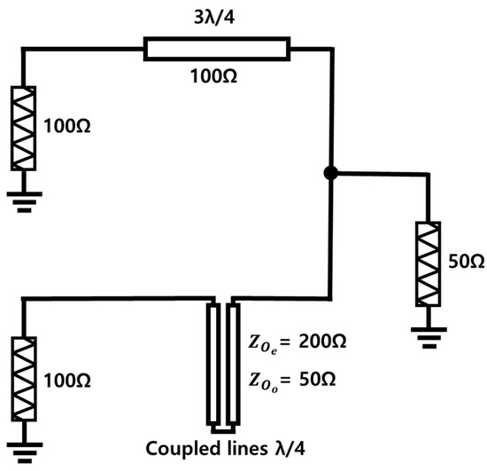
Figure 2.
Schiffman phase shifter.
Figure 3 presents the phase difference responses of the Schiffman phase shifter across a frequency range of 0 to 3 GHz for three different configurations. The substrate was FR-4 with a 2.4 mm height and εr of 4.2. Each configuration was characterized by unique even-mode and odd-mode impedances, with the corresponding geometrical parameters listed in the table. The red, green, and blue curves represent phase difference 1, 2, and 3, respectively. Each trace exhibited three distinct frequency points where a 90° phase shift was achieved. Phase difference 1 (red curve): with = 200 Ω and = 50 Ω, the 90° phase difference occurred at approximately 1 GHz, 1.8 GHz, and 2.6 GHz. Green curve: for = 400 Ω and = 25 Ω, 90° crossings were observed at around 0.8 GHz, 1.8 GHz, and 3 GHz, showing a steeper and more frequency-sensitive behavior. Blue curve: with = 250 Ω and = 40 Ω, a 90° phase shift was achieved at approximately 0.9 GHz, 1.8 GHz, and 2.8 GHz. Among the three configurations, Trace 1 (red) demonstrated the most suitable performance for our design goals, as it effectively covered the low band (LB), mid band (MB), and high band (HB) frequency ranges. Additionally, its impedance and geometry values were well within the practical limits of standard PCB fabrication processes (minimum trace width and spacing of 150 μm), making it a more reliable and manufacturable solution.
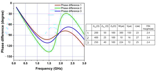
Figure 3.
Phase responses of the Schiffman phase shifter.
The adopted Schiffman phase shifter enabled a 90-degree phase shift across the three frequency bands, supporting the triple-band Doherty power amplifier operation. While these frequencies align with common communication standards, the phase shifter’s design inherently linked the bands through its electrical length and impedance characteristics. However, this relationship was not rigid, and the methodology can be adapted to different frequency spacings by adjusting coupled-line parameters.
The geometry of a single microstrip is shown in Figure 4a. Here, the conductor, with a width of W1, was printed on a grounded dielectric substrate. The thickness of the substrate is H, and its relative permittivity is εr. L represents the length of the line, and T denotes the thickness of the microstrip line. The geometry of the coupled microstrip line is illustrated in Figure 4b. Two conductors, each with a width, W2, were printed parallel to the substrate, with spacing, S, between them. For the regular PCB fabrication process, we followed the recommended rules that state the minimum values for W2 and S should be 150 µm. We used an FR-4 substrate with a dielectric constant of 4.2, a height of 2.4 mm, and line dimensions of W2 = 300 µm and S = 150 µm to realize the conditions of = 200 Ω and = 50 Ω at 1.8 GHz.
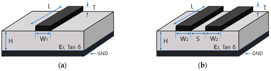
Figure 4.
Microstrip lines. (a) Geometry of a single microstrip line. (b) Geometry of coupled microstrip lines.
2.3. Proposed Doherty Power Amplifier
Based on the above explanation, the triple-band Doherty topology introduced in this paper incorporates a carrier amplifier and a peaking amplifier, utilizing a 3λ/4 line and a 90-degree coupled line configuration, as depicted in Figure 5.
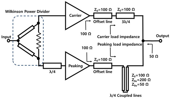
Figure 5.
Proposed Doherty power amplifier.
A Wilkinson power divider, a carrier amplifier, and a peaking amplifier were designed to have broadband characteristics that cover all three operating frequencies. Offset lines were introduced in the output path to provide an open circuit condition for the peaking amplifier and compensation for the phase difference between the two paths [15]. The outputs of the carrier and the peaking amplifiers were matched at 100 Ω. The characteristic impedance of the uniform transmission line was 100 Ω. The characteristic impedance of the coupled lines was 100 Ω with of 200 Ω and of 50 Ω. Both transmission lines, each with a characteristic impedance of 100 Ω, enabled a parallel connection of the carrier and peaking amplifiers in the high-power region. This parallel combination effectively transformed the two 100 Ω impedances at the amplifier outputs into a 50 Ω load.
Figure 6 illustrates the simulated variation in the magnitude of load impedances as a function of normalized currents for both the carrier and peaking paths in the proposed Doherty power amplifier [16]. At low normalized current levels (below 0.5), the carrier amplifier dominated the operation, and the peaking amplifier remained inactive, resulting in a constant carrier load impedance of about 200 Ω (twice of the matching impedance 100 Ω). As the normalized current increased beyond this threshold, the peaking amplifier became active, causing a rapid drop in the peaking load impedance due to load modulation. This behavior was essential to the Doherty architecture, enabling efficiency enhancement at back-off power levels. Figure 6 shows the representative load modulation at 0.8 GHz, 1.8 GHz, and 2.9 GHz, where the load modulation seemed assured among near frequencies.
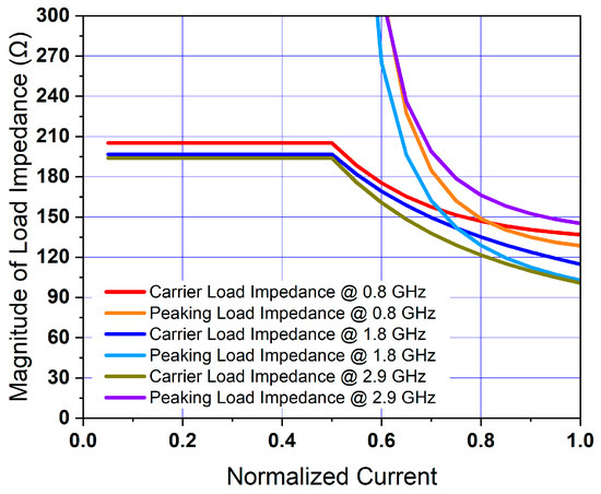
Figure 6.
Load modulation of the proposed Doherty amplifier.
The 90-degree Schiffman phase shifter played a critical role in enhancing the efficiency and broad frequency range operation of the triple-band Doherty power amplifier. The phase shifter facilitated a precise 90-degree phase shift across three distinct frequency bands, enabling optimal phase alignment for each band. This precise phase shifting was essential for combining the outputs of the carrier and peaking amplifiers in a manner that maximized efficiency at different frequencies, ensuring the DPA operated efficiently across all three bands. The performance goals included an output power of 32 dBm with 50% efficiency at saturation and an efficiency of 35% at a 6-dB back-off.
3. Design Procedure
To rigorously verify the proposed theory, all circuits were fabricated on an FR-4 substrate with a dielectric constant of 4.2, a height of 2.4 mm, and a loss tangent of 0.01. The target frequency range extended from 0.6 GHz to 3 GHz, encompassing the uplink bands for 3G, LTE, and 5G cellular communication systems.
The proposed DPA was designed as a multi-band PA using 6 W GaN on SiC HEMT devices (Qorvo TGF2965-SM, Greensboro, NC, USA) [17]. A schematic of the entire DPA design is illustrated in Figure 7. The topologies for the carrier and peaking amplifiers were identical, except for their bias conditions. The carrier amplifier was biased in class AB mode, while the peaking amplifier operated in class C mode.
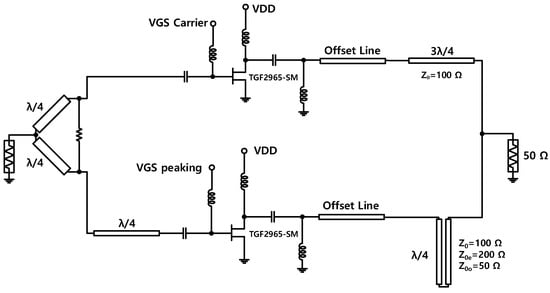
Figure 7.
Schematic of the designed Doherty power amplifier.
The post-layout electromagnetic (EM) simulation results of the power amplifier (PA) are shown in Figure 8. We applied 20 V for the drain, because the minimum valid drain voltage of the transistor model was 20 V. The simulated drain efficiency and gain versus output power within the frequency ranges of LB 0.8 GHz, MB 1.6 GHz, and HB 2.2 GHz are depicted. The proposed DPA achieved drain efficiencies at a saturation of 45% for LB, 50% for MB, and 50% for HB. We achieved gains of around 10 dB for each band. The gate bias voltage for the carrier amplifier was set to −2.5 V to obtain a quiescent current of 40 mA, while the gate bias voltage for the peaking amplifier was set to −3.7 V with no current consumption. The simulation results indicate that the saturated output power () reached 37 dBm, 36 dBm, and 37 dBm for the low band, mid band, and high band, respectively.
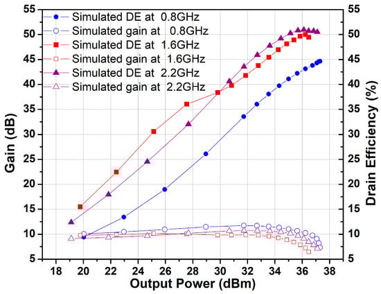
Figure 8.
Simulated drain efficiency (DE) and gain versus output power within the LB, MB, and HB frequency ranges under a 20 V drain bias.
4. Measurement Results
The fabricated image of the proposed DPA, shown in Figure 9, had an area of 79 × 95 mm2. This topology was simulated with a 20 V supply voltage due to the valid model range. However, during the measurement process, we applied a 12 V supply voltage to achieve proper output power for mobile applications and to avoid overheating. When operating at the low-band frequency of 0.8 GHz, the carrier amplifier’s gate bias was −2.8 V, and the peaking amplifier’s gate bias was −3.9 V. At the mid-band frequency of 1.6 GHz, the carrier amplifier maintained a gate bias of −2.65 V, while the peaking amplifier operated at a gate bias of −3.7 V. Similarly, at the high-band frequency of 2.2 GHz, the carrier amplifier’s gate bias remained at −2.5 V, with the peaking amplifier’s gate set at −3.7 V. At 0.8 GHz, the amplifier drew 410 mA at a 12 V drain bias supply voltage, resulting in a power consumption of 4.92 W. At 1.6 GHz, it consumed 3.17 W with a current draw of 264 mA, and at 2.2 GHz, it drew 327 mA, leading to a power consumption of 3.92 W.
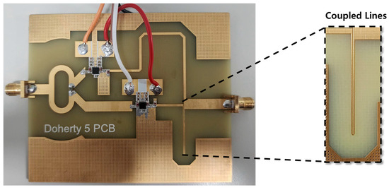
Figure 9.
Fabricated Doherty power amplifier.
A signal generator was used to generate the required input signal, and a driver amplifier was placed between the signal generator and the fabricated DPA to amplify the input power. A spectrum analyzer and a power meter were utilized to monitor the output signal, with an attenuator inserted before it, as shown in Figure 10.
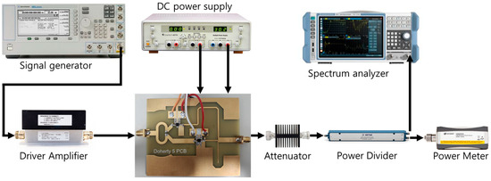
Figure 10.
Measurement setup of the Doherty power amplifier.
The measured S-parameters of the fabricated DPA are shown in Figure 11. A supply voltage of 12 V was applied. As a result of the Schiffman phase shifter, we achieved a triple-band operation with a gain of over 10 dB. The S(1,1) result indicates the input reflection coefficient, consistently remaining around −10 dB within the desired bands.
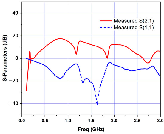
Figure 11.
Measured S-parameters of the proposed Doherty power amplifier.
Figure 12 presents the power sweep results at 0.8 GHz, 1.6 GHz, and 2.2 GHz for both the Doherty mode and the class AB mode with a supply voltage of 12 V. Figure 12a shows low band performance compared to the class AB mode. The drain efficiency was over 50%, providing an output power of 34 dBm. At a 6-dB output back-off, the drain efficiency reached 43%. At the mid-band 1.6 GHz frequency, the drain efficiency exceeded 47%, resulting in an output power of 32 dBm. In the 6-dB output back-off region, the drain efficiency was 35%, as depicted in Figure 12b. Also, at the high band 2.2 GHz, illustrated in Figure 12c, a 50% drain efficiency was achieved with a 33 dBm output power. Even in the 6-dB output back-off region, a drain efficiency close to 40% was still maintained. The three bands exhibited a nearly 10 dB gain alongside the explained drain efficiency trends. The measured frequencies differed from the simulated ones in Figure 6 due to parasitic effects from the PCB layout, which altered the impedance and load modulation trajectory. Structural variations in the coupled-line sections (width, spacing, length) also affected the EM behavior. Additionally, the transistor gain characteristics and fabrication tolerances in the Schiffman phase shifter contributed to the observed frequency shift.
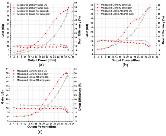
Figure 12.
Measured Doherty amplifier drain efficiency and measured class AB amplifier drain efficiency versus output power within the desired frequency ranges. (a) Low band, 0.8 GHz; (b) mid band, 1.6 GHz; (c) high band, 2.2 GHz.
The simulated saturation output power was expected to reach 37 dBm, while the measured results were lower at 32–34 dBm. Notably, the simulation used a 20 V supply, because the transistor model is valid for voltages above 20 V. However, the prototype was tested at 12 V to suit mobile applications and reduce heating, inherently lowering the output power. Since it was intended for mobile use, it was operated with a 12 V power supply.
When comparing the results of the proposed Doherty power amplifier with those of the class AB mode PA, it was confirmed that the triple-band Doherty amplifier operated effectively. In summary, this topology serves as the optimal foundation for cellular applications, enabling the utilization of multiple bands with a single power amplifier. It leverages the Doherty architecture and consistently delivers efficiency boosting performance across various frequency bands. Moreover, a 12 V supply voltage can be utilized in cellular applications using a dynamic boost DC-DC converter, similar to how recent mobile amplifiers utilize a dynamic buck converter for envelope tracking.
Table 1 presents a comparison with previously published two- and three-band DPAs. The results demonstrate that the designed DPA achieved sufficient performance while operating at a low DC bias voltage. Our objective was to develop a triple-band DPA for mobile applications. Based on the proposed results, this concept serves as a promising starting point for communication researchers aiming to develop wideband solutions. The proposed DPA demonstrates triple-band operation with efficient amplification using a compact design enabled by a Schiffman phase shifter and optimized biasing, achieving up to a 50% drain efficiency at a lower 12 V bias compared to the 28 V in prior works, making it suitable for mobile applications.

Table 1.
Comparison with published multi-band DPAs.
According to our investigation, to ensure transparency and technical rigor, we incorporated detailed information about the transistor, Qorvo TGF2965-SM GaN on SiC HEMT, along with its validated model specifications. Although the model is officially supported for operation at 32 V, our target application required operation at 12 V. To address this, the amplifier was designed using the model at 20 V, where its gain was at least 10 dB, and subsequently tested at 12 V. Although some discrepancies between simulations and measurements were observed, the measurement results were sufficient to demonstrate the triple-band operation of the DPA with a Schiffman phase shifter.
5. Conclusions
This article introduces a novel concept for the mobile communication sector: a triple-band Doherty power amplifier topology designed to operate across multiple bands within a single unit. It was centered at a frequency of 1.8 GHz and utilizes a Schiffman phase shifter to achieve performance across three distinct frequency bands. This triple-band Doherty power amplifier aims to enhance power efficiency across low-band, mid-band, and high-band cellular uplink frequencies. The adopted Schiffman phase shifter played a significant role in the configuration of this triple-band DPA, with simulation results demonstrating good performance and efficiency. The market for mobile communications, covering multiple frequency bands, is expanding. Within this context, triple-band or multi-band Doherty amplifiers can support PA operations across three or more frequency bands while maintaining good efficiency at back-off power levels. This approach can simultaneously reduce costs and sizes while ensuring energy-efficient operations.
Author Contributions
Conceptualization, J.K. and D.-H.L.; investigation, I.H.H.M. and D.-H.L.; formal analysis, I.H.H.M.; writing—original draft preparation, I.H.H.M.; writing—review and editing, D.-H.L.; supervision, G.J. and D.-H.L.; funding acquisition, D.-H.L. All authors have read and agreed to the published version of the manuscript.
Funding
This research was funded by the Campus Research Fund through Hanbat National University in 2021.
Data Availability Statement
The original contributions presented in this study are included in the article. Further inquiries can be directed to the corresponding author.
Conflicts of Interest
The authors declare no conflicts of interest.
References
- Grebennikov, A.; Wong, J. A Dual-Band Parallel Doherty Power Amplifier for Wireless Applications. IEEE Trans. Microw. Theory Tech. 2012, 60, 3214–3222. [Google Scholar] [CrossRef]
- Saad, P.; Andersson, K.; Fager, C.; Colantonio, P.; Piazzon, L.; Giannini, F. Design of a Concurrent Dual-Band 1.8–2.4-GHz GaN-HEMT Doherty Power Amplifier. IEEE Trans. Microw. Theory Tech. 2012, 60, 1840–1849. [Google Scholar] [CrossRef]
- Wen, H.; Feng, W.; Zhu, H.; Che, W.; Xue, Q. Design of Dual-band High Efficiency and Linearity Doherty Power Amplifier. In Proceedings of the 2022 International Conference on Microwave and Millimeter Wave Technology (ICMMT), Harbin, China, 12–15 August 2022. [Google Scholar]
- Bathich, K.; Gruner, D.; Boeck, G. Analysis and Design of Dual-Band GaN HEMT Based Doherty Amplifier. In Proceedings of the 2011 6th European Microwave Integrated Circuit Conference (EuMIC), Manchester, UK, 10–11 October 2011; pp. 248–251. [Google Scholar]
- Colantonio, P.; Feudo, F.; Giannini, F.; Giofrè, R.; Piazzon, L. Design of a dual-band GaN Doherty amplifier. In Proceedings of the 18th International Conference on Microwaves, Radar and Wireless Communications, Vilnius, Lithuania, 14–16 June 2010; pp. 1–4. [Google Scholar]
- Rawat, K.; Gowrish, B.; Ajmera, G.; Kalyan, R.; Basu, A.; Koul, S.; Ghannoushi, F.M. Design strategy for tri-band Doherty power amplifier. In Proceedings of the 2014 Wireless and Microwave Conference (WAMICON), Tampa, FL, USA, 5–6 June 2014; pp. 1–3. [Google Scholar]
- Bhardwaj, S.; Kitchen, J. Broadband Parallel Doherty Power Amplifier in GaN for 5G Applications. In Proceedings of the 2019 IEEE Topical Conference on RF/Microwave Power Amplifiers for Radio and Wireless Applications (PAWR), Orlando, FL, USA, 20–23 January 2019; pp. 1–3. [Google Scholar]
- Xiong, D.; Liu, C.; Huang, L.; Wang, H. A 3.3–3.7 GHz Broadband Doherty Power Amplifier. In Proceedings of the 2021 13th International Symposium on Antennas, Propagation and EM Theory (ISAPE), Zhuhai, China, 1–4 December 2021; pp. 1–3. [Google Scholar]
- Jarndal, A.; Hamza, K.H. On the Design of Broadband Doherty Power Amplifier for 5G Applications. In Proceedings of the 2022 International Conference on Electrical and Computing Technologies and Applications (ICECTA), Ras Al Khaimah, United Arab Emirates, 23–25 November 2022; pp. 370–373. [Google Scholar]
- Nasri, A.; Estebsari, M.; Toofan, S.; Piacibello, A.; Pirola, M.; Camarchia, V.; Ramella, C. Design of a Wideband Doherty Power Amplifier with High Efficiency for 5G Application. Electronics 2021, 10, 873. [Google Scholar] [CrossRef]
- Schiffman, B.M. A New Class of Broad-Band Microwave 90-Degree Phase Shifters. IRE Trans. Microw. Theory Tech. 1958, 6, 232–237. [Google Scholar] [CrossRef]
- Guo, Y.-X.; Zhang, Z.-Y.; Ong, L.C. Improved wide-band Schiffman phase shifter. IEEE Trans. Microw. Theory Tech. 2006, 54, 1196–1200. [Google Scholar]
- Amin, F.; Liu, L.; Liu, Y.; Zhao, Y. Dual-Band Schiffman Phase Shifter with Large Frequency Ratio and Wide Bandwidths. In Proceedings of the 2023 53rd European Microwave Conference (EuMC), Berlin, Germany, 19–21 September 2023; pp. 54–57. [Google Scholar]
- Quirarte, J.L.R.; Starski, J.P. Novel Schiffman phase shifter. IEEE Trans. Microw. Theory Tech. 1993, 41, 9–14. [Google Scholar] [CrossRef]
- Kim, B. Doherty Power Amplifiers: From Fundamentals to Advanced Design Methods; Academic Press: Cambridge, MA, USA, 2018. [Google Scholar]
- Chen, S.; Xue, Q. Optimized Load Modulation Network for Doherty Power Amplifier Performance Enhancement. IEEE Trans. Microw. Theory Tech. 2012, 60, 3474–3481. [Google Scholar] [CrossRef]
- TGF2965-SM: 0.03–3 GHz, 5 Watt, 32 V, 50 Ohm GaN RF Input-Matched Transistor. Available online: https://www.qorvo.com/products/p/TGF2965-SM (accessed on 25 May 2025).
- Cao, Y.; Chen, K. Hybrid Asymmetrical Load Modulated Balanced Amplifier with Wide Bandwidth and Three-Way-Doherty Efficiency Enhancement. IEEE Microw. Wireless Compon. Lett. 2021, 31, 721–724. [Google Scholar] [CrossRef]
Disclaimer/Publisher’s Note: The statements, opinions and data contained in all publications are solely those of the individual author(s) and contributor(s) and not of MDPI and/or the editor(s). MDPI and/or the editor(s) disclaim responsibility for any injury to people or property resulting from any ideas, methods, instructions or products referred to in the content. |
© 2025 by the authors. Licensee MDPI, Basel, Switzerland. This article is an open access article distributed under the terms and conditions of the Creative Commons Attribution (CC BY) license (https://creativecommons.org/licenses/by/4.0/).