1. Introduction
Strain engineering, as an important method for enhancing device performance, has been widely implemented in conventional bulk silicon MOSFETs and has become an indispensable element of CMOS scaling. Intentional channel stress, introduced through methods such as stress memorization technique (SMT) [
1], embedded lattice-mismatched SiGe [
2], and high-stress contact etch stop layers (CESL) [
3], can significantly enhance device performance. However, due to factors such as layout-dependent effects or unintentional process-induced stress, device performance may vary [
4]. Previous studies have shown that unintentional stress caused by STI can lead to performance variations of up to 19% at the 0.18 μm technology node [
5]. Therefore, investigating the impact of STI stress on device performance is crucial.
Since the 22 nm technology node, FinFET technology has been widely adopted in advanced low-power and high-performance applications, replacing traditional planar silicon devices. To further improve device performance, FinFETs also incorporate techniques similar to strain engineering. STI and CESL stress engineering techniques remain effective means of improving carrier mobility and drive current in FinFET devices, even at technology nodes below 20 nm. STI-induced stress originates from mechanical interactions between the isolation trench and the active region and can be modulated through factors such as STI recess depth and active layout geometry. CESL stress, introduced via high-stress nitride liners deposited over the gate stack, can be adjusted to induce uniaxial tensile or com-pressive stress, enhancing electron or hole mobility depending on the device type. These methods have been widely adopted in modern FinFET technology as performance boosters when conventional scaling reaches its limits [
6,
7]. However, as technology nodes continue to scale down and FinFET structures become taller and narrower, device characteristics have become increasingly sensitive to asymmetric stress. Even with the same gate length (L) and Fin width (W), performance variation can still occur due to asymmetric stress. This is because asymmetric STI stress causes inconsistent carrier mobility within the Fin channel, resulting in variations in device current [
8]. Despite the significant impact of asymmetric STI stress on FinFET performance fluctuations, this effect has not been thoroughly investigated.
Previous studies have demonstrated that STI-induced stress plays a critical role in FinFET performance, where the geometry of the STI recess significantly alters the local stress distribution and thus affects carrier transport characteristics. For example, variations in STI etch profiles can lead to measurable differences in drive current, especially for n-type FinFETs where tensile stress enhances electron mobility [
9]. In addition, CESL stress engineering has been shown to further modulate stress states in FinFET structures, offering additional degrees of freedom for performance tuning [
10]. However, these studies typically consider symmetric device structures and stress environments, such as balanced STI recess or uniformly applied CESL layers. In contrast, asymmetric stress conditions—common in advanced layouts due to design constraints or process variations—remain underexplored. In this work, we focus on isolated FinFET devices under deliberately introduced asymmetric STI-induced stress, aiming to reveal the unique impact on device-level electrical characteristics.
To accurately capture the relationship between asymmetric STI stress and the Fin structure, this paper employs TCAD simulations to model stress distribution and analyze the impact of asymmetric stress on 10 nm FinFETs. The study reveals that as the Fin width decreases, device performance deteriorates significantly under asymmetric STI stress, peaking at W = 6 nm. Additionally, the angle of the Fin body also affects the impact of asymmetric STI stress. The closer the Fin body angle is to 90°, the smaller the effect of asymmetry. Since asymmetric STI stress primarily affects the sidewall channels of the Fin and has a weaker impact on the top channel, this paper proposes utilizing CESL stress engineering to amplify the current contribution from the top channel, thereby mitigating the adverse effects of asymmetric STI stress on device performance [
8].
3. Mechanical Stress Distribution and Different Shape of Fin
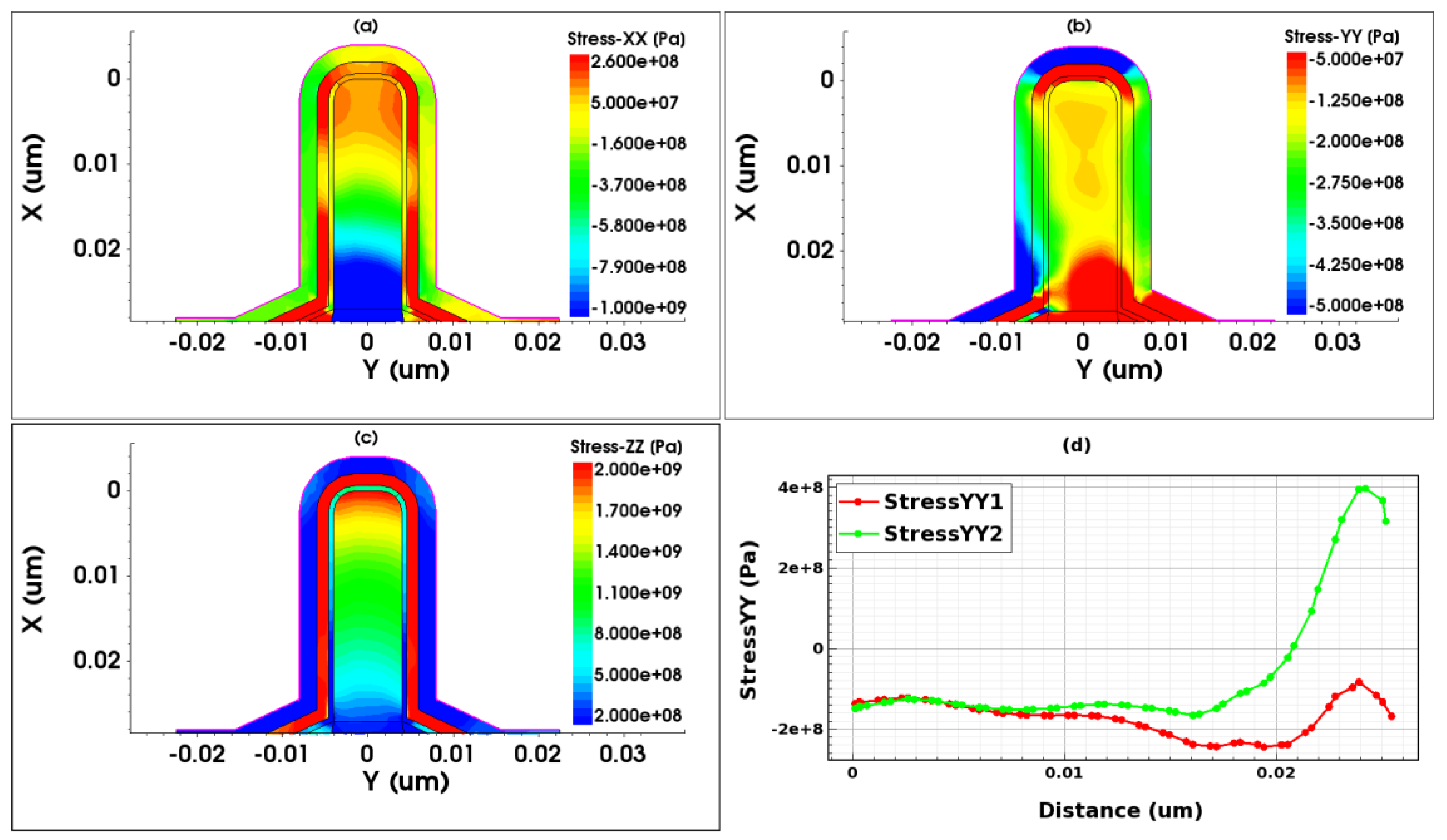
The stress distribution in the Fin channel under asymmetric STI stressors is shown in
Figure 2. The Fin channel exhibits a significant asymmetric stress profile, primarily concentrated near the sidewall channels, with minimal impact on the top channel. This phenomenon is mainly attributed to the tall and narrow geometry of the Fin. Since STI is deposited along the channel direction, the asymmetric mechanical stress form STI has the greatest impact in the longitudinal direction, while the mechanical stress in the vertical direction remains nearly symmetric. The simulated mechanical stress distribution along both sidewalls of the Fin in the longitudinal direction is shown in
Figure 2d, the distance refers to the x-direction along the vertical axis of the Fin, with the cutline positioned at a y-coordinate of 26.5 nm, perpendicular to the channel, the mechanical stress deviation between the two sidewalls reaches approximately 500 MPa. This results in carrier mobility variations in the sidewall channel, ultimately affecting device performance.
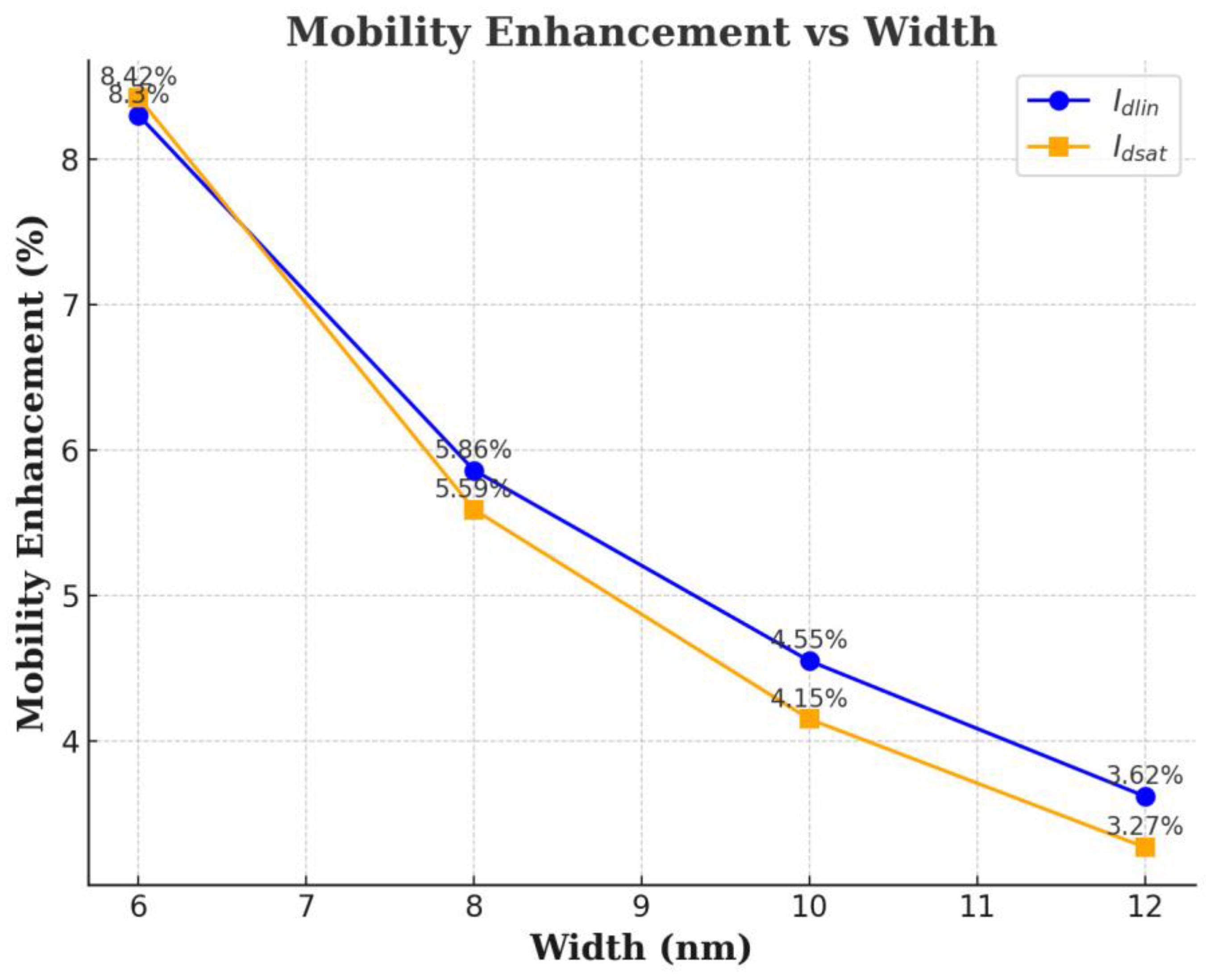
The stress distribution in the Fin channel also depends on the its width, as shown in
Figure 3. Different Fin widths result in varying degrees of impact from asymmetric stress on device performance. The carrier mobility enhancement (∂
μtotal) is used to characterize the offset in drain current caused by asymmetric stress. As shown in
Figure 3, ∂
μtotal increases from 3.62% to 8.30% in the linear region and from 3.27% to 8.42% in the saturation region as the Fin width decreases from 12 nm to 6 nm. As the Fin width increases, the mobility enhancement decreases significantly, indicating that tall and narrow Fin structures are more severely affected by asymmetric stress than wider Fins.
As shown in
Figure 3, the mobility enhancement trends differ between the linear and saturation regions. This is because
Idlin, which is extracted in the linear region, is more directly influenced by low-field mobility variations, making it more sensitive to stress-induced changes. In contrast,
Idsat in the saturation region is governed by high-field effects, such as velocity saturation and channel length modulation, which can diminish the apparent impact of mobility changes. These physical distinctions result in the different trends observed between
Idlin and
Idsat under various stress conditions.
As shown in
Figure 2, larger compressive stress extends from the STI to the sidewall channel of the Fin, diffusing toward the top and central regions. The asymmetric STI stress is mainly concentrated in the sidewall channel, with relatively little effect on the top channel. Consequently, as the Fin width continues to decrease, the proportion of current through the sidewall channel increases, leading to greater mobility enhancement and a stronger impact of asymmetric stress on the FinFET performance.
Additionally, a significant upward trend in mobility enhancement is observed for FinFETs with W = 6 nm. This is because, when the Fin is sufficiently wide, the top channel shows no significant dependence on asymmetric stress. The Stress YY of FinFETs with W = 6 nm and W = 8 nm is shown in
Figure 4a,b, respectively. This asymmetry is primarily attributed to the two stress sources at the Fin corners, with a weaker influence on channel current. However, as the Fin width decreases, the stress sources at the Fin corners overlap, causing the top channel to become increasingly affected by asymmetric stress, becoming more similarly to the sidewall channel. This results in a sharp increase in mobility enhancement at W = 6 nm.
Figure 4c,d show the distribution of Stress YY in the top channel of FinFETs with W = 6 nm and W = 8 nm, respectively. It can be observed that stress asymmetry in the top channel of the W = 6 nm FinFET is significantly higher than that of the W = 8 nm FinFET. These results indicate that as technology advances, Fins are evolving to become taller and narrower, making FinFET performance increasingly sensitive to asymmetric stress.
Moreover, it is well known that the Fin body angle also affects the performance of FinFET devices. Studies have shown that as the Fin body angle approaches 90°, both the drain-induced barrier lowering (DIBL) and subthreshold swing (SS) decrease accordingly [
13,
14]. Therefore, the research also investigated the relationship between the Fin body angle and the asymmetric stress introduced by STI.
As shown in
Figure 5, as the top width of the Fin decreases from 8 nm to 6 nm, ∂
μtotal increases from 5.59% to 7.45% in the saturation region, and from 5.86% to 7.65% in the linear region. This increase is primarily due to the narrowing of the FinFET top as the Fin body angle decreases. The trend of mobility enhancement mirrors the behavior observed with changes in Fin width. As the Fin body angle decreases, the impact of asymmetric stress on FinFET performance becomes more significant. A noticeable local decrease in mobility enhancement at a Fin body angle corresponding to a top width of 7 nm suggests a potential structural or electrostatic optimization at this geometry—possibly due to stress redistribution or increased surface scattering—which we plan to investigate further in future work. In practice, however, FinFET structures are influenced by the well-known miscut step phenomenon, rather than being ideally un-tapered and straight [
15,
16]. As a result, the deviation of the Fin body angle from 90° further exposes the device to the effects of asymmetric stress.
In addition to Fin width and CESL stress, the effect of Fin height on asymmetric stress performance is also worth noting. Since the STI-induced asymmetric stress primarily affects the sidewalls of the Fin channel, a taller Fin increases the relative contribution of the sidewall channel to the total current. This amplifies the influence of stress asymmetry on carrier transport and device variability. A more detailed investigation of Fin height effects on asymmetric stress will be conducted in our future work.
4. Mitigating the Impact of STI-Induced Asymmetric Stress
The impact of asymmetric stress introduced by STI on FinFETs is primarily concentrated in the sidewall channel, while the top channel current acts to counterbalance this effect. Therefore, to mitigate the effect of STI-induced asymmetric stress on device performance, a feasible process to enhance the top channel current is needed. Studies have shown that CESL stress engineering can significantly improve device performance [
17].
As the first material layer deposited above the FinFET structure, CESL can efficiently transfer its intrinsic stress to the silicon channel. Due to the unique structure of FinFETs, CESL-induced stress is more effectively coupled to the top channel, while its influence on the sidewall channel is relatively weak [
12]. This stress redistribution reduces the overall impact of STI-induced asymmetry on device behavior.
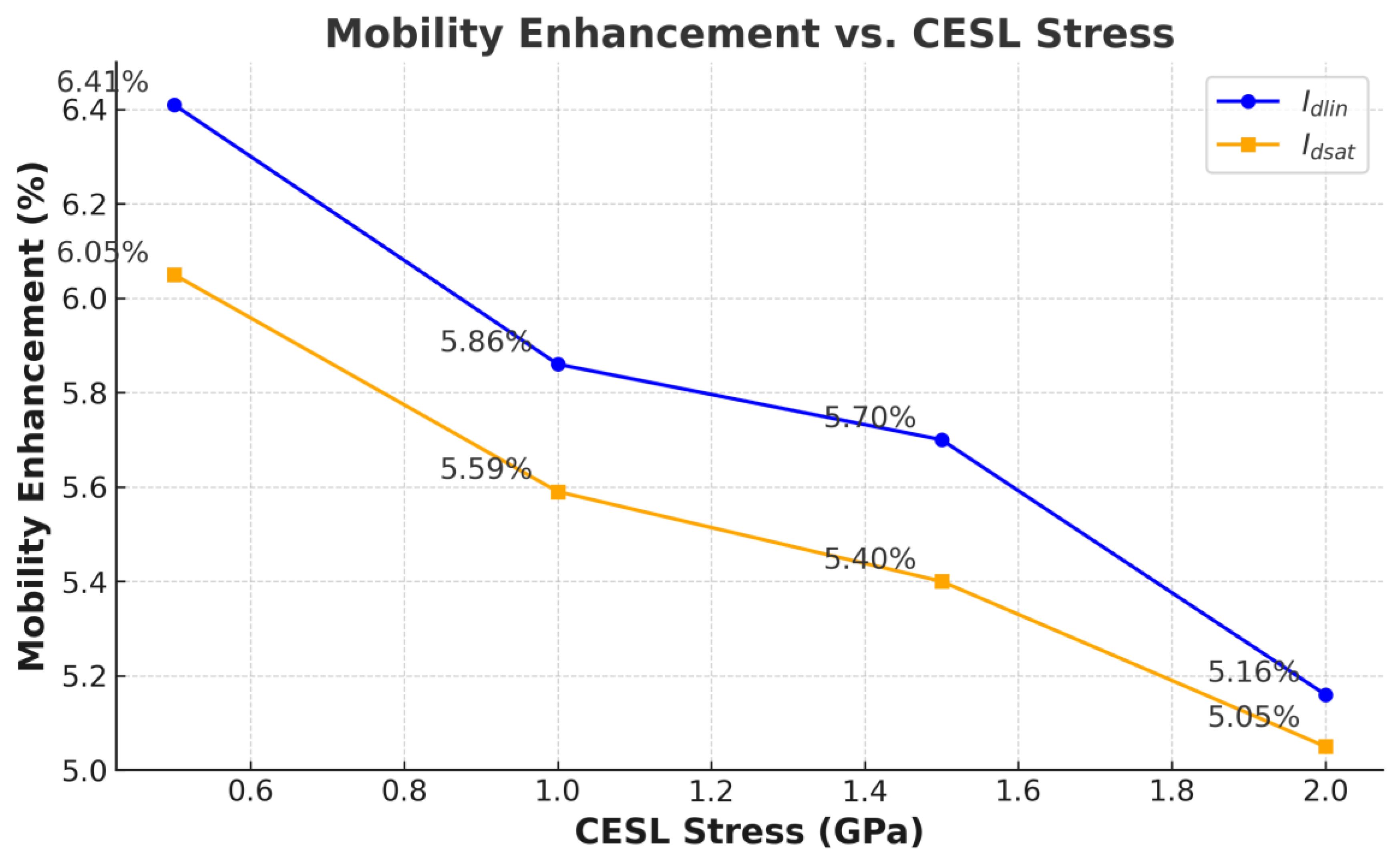
Figure 6 illustrates the dependence of mobility enhancement in the linear and saturation regions on the magnitude of CESL stress under different stress engineering conditions. As the intrinsic stress of CESL increases, the observed mobility enhancement decreases significantly. A lower CESL stress leads to higher measured mobility enhancement, as the CESL stress helps balance the STI-induced asymmetry. Therefore, the mobility enhancement does not reflect performance improvement, but rather stress imbalance. When the intrinsic stress of the CESL increases from 500 MPa to 2.0 GPa, the mobility enhancement decreases from 6% to 5%. The 2.0 GPa stress of the CESL contributes to a 20% improvement in device stability, reflecting better stress balance and reduced process-induced performance variation. These results demonstrate that CESL stress engineering is an effective approach to mitigating STI-induced asymmetric stress.
In fabrication processes, asymmetric stress introduced by STI is inevitable due to factors such as layout. However, thanks to the geometry of the Fin structure, CESL-induced stress is typically more symmetric. Therefore, using CESL stress engineering to counteract STI-induced asymmetric stress is considered feasible in actual manufacturing processes.
5. Conclusions
This paper provides an overview of the impact of STI-induced asymmetric stress on FinFET device performance through TCAD simulations. Due to the asymmetric stress introduced by STI, the stress distribution along the sidewall channels of the Fin becomes asymmetric, leading to variations in the carrier mobility caused by mechanical stress and ultimately degrading device stability. Furthermore, as the Fin width continues to decrease, the performance fluctuation caused by the asymmetric stress becomes more pronounced. At W = 6 nm, the maximum value of ∂μtotal in the saturation region reaches 8.42%.
In addition, as the Fin body angle deviates from 90° and the upper section narrows, asymmetric stress further amplifies performance variations, with ∂μtotal peaking at 7.65%. To mitigate these variations, CESL stress engineering is applied to counterbalance STI-induced asymmetric stress. A CESL stress of 2.0 GPa results in approximately 20% improvement in device stability, demonstrating the effectiveness of CESL stress engineering in suppressing performance fluctuation


