Article

Vision-Based Structural Adhesive Detection for Electronic Components on PCBs

1
Jiangsu Province Engineering Research Center of Integrated Circuit Reliability Technology and Testing System, Wuxi University, Wuxi 214105, China
2
Wuxi Tailianxin Technology Co., Ltd., Wuxi 214000, China
*
Authors to whom correspondence should be addressed.
Electronics 2025, 14(10), 2045; https://doi.org/10.3390/electronics14102045 (registering DOI)
Submission received: 24 April 2025 / Revised: 8 May 2025 / Accepted: 10 May 2025 / Published: 17 May 2025
(This article belongs to the Section Computer Science & Engineering)

Abstract

:
Structural adhesives or fixing glues are typically applied to larger components on printed circuit boards (PCBs) to increase mechanical stability and minimize damage from vibration. Existing work tends to focus on component placement verification and solder joint analysis, etc. However, the detection of structural adhesives remains largely unexplored. This paper proposes a vision-based method for detecting structural adhesive defects on PCBs. The method uses HSV color segmentation to extract PCB regions, followed by Hough-transform-based morphological analysis to identify board features. The perspective transformation then extracts and rectifies the adhesive regions, and constructs an adhesive region template by detecting the standard adhesive area ratio in its corresponding adhesive region. Finally, template matching is used to detect the structural adhesives. The experimental results show that this approach can accurately detect the adhesive state of PCBs and identify the qualified/unqualified locations, providing an effective vision-based detection scheme for PCB manufacturing. The main contributions of this paper are as follows: (1) A vision-based structural adhesive detection method is proposed, and its detailed algorithm is presented. (2) The developed system includes a user-friendly visualization interface, streamlining the inspection workflow. (3) Actual experiments are performed to evaluate this study, and the results validate its effectiveness.

1. Introduction

Automatic and intelligent equipment is widely used in various industries to improve production efficiency and reduce production costs. One of the key components is the processor system, usually presented as a printed circuit board (PCB). For example, an automotive control system consists of several PCB modules [1], each with a specific function (driving calculation, data communication, data storage, etc.). Thus, a PCB is populated with various electronic components such as resistors, capacitors, transistors, and chips. However, when used in harsh environments such as aircraft and vehicles, random vibrations and high-intensity shocks often occur. They can significantly degrade the performance or even cause a failure of the electronic components on PCBs [2]. As a result, structural or fastening adhesives are typically applied to larger components to improve mechanical stability and minimize damage from vibration [3]. Epoxy and silicone adhesives are commonly used to fix components to PCBs [4].
Multi-stage detection is required in the PCB manufacturing process to ensure the functional reliability of the entire equipment [5]. Different detections are designed in production lines, and defect detection is one of the critical steps. Although approaches have been proposed, they focus more on the detection of missing components [6], soldering defects [7], etc. Less work is dedicated to the detection of structural adhesives on PCBs. One aspect is the use of the automatic adhesive-dispensing machine, which can simultaneously dispense and inspect the results. Another aspect is to integrate this adhesive detection step into another manufacturing process [6]. However, if a PCB does not undergo the two processes above, or if its structural adhesives are applied manually (by a worker), an additional detection step is a must.
The detection of structural adhesives usually faces several problems. Firstly, due to negligence, adhesives may not be present at the appropriate location of electronic components [7], which is the most serious defect. Secondly, the amount of adhesive is insufficient and does not meet the standards. These two examples cover almost all possible cases in manual operations. Other cases—dispensing adhesive in the wrong place or dispensing too much—are rare and less serious than the situations above, which are acceptable and usually considered to be within specification. This paper, therefore, focuses on two defects: the absence of adhesive and insufficient adhesive.
Vision-based methods are usually used for adhesive defect detection. Conventional vision processing depends on less hardware computational resources. It usually combines several methods at different stages and optimizes several parameters to achieve satisfactory results [8], which requires considerable experience in the field. Some practical tools, such as OpenCV and Halcon, make image processing easy. In recent years, deep neural network technology has developed rapidly and is widely used in object detection and recognition [9]. This approach generally requires a large dataset for training and depends on high-performance hardware [10], such as a GPU, NPU, etc., which requires a higher budget. A key advantage is a user-friendly interface, especially with current neural network models [11], such as the R-CNN model series and YOLO models [12]. Given the lack of large training datasets and limited cost, this work applies conventional image processing based on the OpenCV library.
This paper’s motivation is clear: (1) Existing work on PCB detection focuses exclusively on defects, such as missing components and soldering defects. Less work is directly relevant to adhesive detection. This work focuses squarely on the issue of adhesive detection. (2) We present a systematic work, including a detection algorithm, operation software, and detection experiments, to realize adhesive detection and provide a reference for other, related research.
This paper proposes a conventional vision-based method for the detection of structural adhesives on PCBs. Image extraction and adhesive region segmentation are first performed. Then, an appropriate threshold is set for each adhesive region, and a standard template library is built. Next, each image can be compared with its corresponding standard template. The detection results depend on the matching results with the template. A visualization software then displays the detection process and results and records the process data. The main contributions of this work are as follows:
(1) A vision-based structural adhesive detection method is proposed, and its algorithmic steps are described in detail.
(2) A visualization software for PCB adhesive detection is developed, which makes the inspection process convenient and fast.
(3) Actual experiments are conducted to evaluate this study, and the results validate its effectiveness.
Detecting structural adhesives on PCBs is a new problem for some specialized PCB-manufacturing industries. In the initial research phase, this paper attempts to solve this problem using conventional vision-based methods. In future research, the deep neural network method will be investigated. The remainder of this paper is organized as follows. Section 2 presents related work. Section 3 introduces the vision-based structural adhesive detection method. Section 4 presents the visualization software and experimental results. Section 5 concludes this work and outlines future research.

2. Related Works

Existing work on PCB detection can be divided into conventional vision and deep learning methods [13]. This research generally focuses on the surface defects of PCBs [14]. A PCB is a human-designed product and usually has precise dimensions. This means that the design information and a standard PCB template can be used in automatic inspection, which greatly improves the detection efficiency. In [15], an efficient similarity measurement method is proposed. It does not require the computation of image features, but relies on measuring the similarity between scene images and their reference images. A template-matching algorithm is used in the alignment process of inkjet [16], which has clear advantages in terms of time, cost, and accuracy. In [17], image registration is the key to improving the processing speed to achieve real-time processing. The utilization of such a template facilitates the accurate detection of defects and the achievement of automatic functions. A PCB reference template is constructed based on the extracted main features, and then these optimized features are probabilistically synthesized and compared with the reference template for defect detection [18]. A pixel-based vector of the regions of interest is used to inspect for excess or insufficient adhesive on PCBs [19]. A support vector machine (SVM) classifier with polynomial and radial basis function kernels has demonstrated excellent performance in tests. Automatic optical inspection (AOI) systems are professional equipment for PCB inspection purposes and are usually provided by manufacturers [20]. The high-resolution imaging function of the AOI is capable of inspecting numerous holes and identifying those that are faulty on a PCB [21], thereby assisting users in the analysis and rectification of faults. However, the utilization of an AOI machine for the detection of structural glue appears to be a somewhat inefficient use of the equipment. Conventional vision methods are therefore employed with great efficiency for the detection of surface defects on PCBs. The distinguishing features of these methods are template registration and pixel comparison, which can be obtained during actual inspection missions with a standard template and pixel information. This class of detection methods can be readily implemented in hardware systems and boasts the advantages of low cost, high efficiency, and ease of maintenance. The present study’s limitation is its focus on electronic components. Few studies have focused on the inspection of structural adhesives on PCBs.
Deep learning methods have been shown to possess the capacity to detect multiple defects simultaneously, and to function effectively in conditions of noise, variations in lighting conditions, and backgrounds with complex textures [22,23]. However, this class of methods generally requires a substantial amount of primary data for model training [24]. In [25], a synthetic PCB dataset is published for the detection, classification, and registration tasks. A Faster RCNN model based on a pre-trained VGG16 network was proposed in [26] for PCB inspection in industrial AOI applications, while a CNN-based method is used in PCB resistor classification and pose prediction [27], and its process node is set at pre-reflow AOI to perform quality control. Other deep network models, such as AKPLNet in [28], can detect PCB defects and achieve better detection accuracy. With an end-to-end framework, YOLO-based methods have significant advantages in PCB inspection [29,30]. A hybrid YOLOv2 model, when combined with Faster RCNN, has been employed for PCB inspection [31], and its enhanced self-adaptation method has been shown to effectively reduce inspection and repair times for online operators [32]. A CDS-YOLO network shows accuracy and real-time performance in detecting defects on PCBs. These YOLO-relevant networks [33,34] are modified from the fundamental YOLO model frameworks and combined with other network structures and adjustments [35]. These modifications are good at enhancing the accuracy, speed, and reliability of the networks in practical detection applications. However, certain detection scenarios require the implementation of bespoke algorithms. For instance, a classification model is proposed that integrates DenseNet169 and ResNet50 [36], achieving high sensitivity in the inspection of minor defects. A lightweight CenterNet with a two-branch vision transformer with local and global attention is tested to detect PCB surface defects [37], improving detection accuracy and inference speed. A Siamese-based network is studied to locate unknown defects in bare PCB images and can be trained with fewer image pairs [38]. These deep learning methods possess a high degree of inspection capability, with the capacity to detect defects on PCBs and demonstrate superior performance. The efficacy of these methods is contingent upon the utilization of image data for training. However, it is important to note that none of these methods offers a dedicated introduction to the structural adhesive detection problem proposed in this paper.

3. Methods

The present study focuses on two defects of PCBs’ structural adhesive: the absence of adhesive and insufficient adhesive. The former defect pertains to the absence of structural adhesive in the predetermined position on PCBs. The second defect pertains to an inadequate adhesive volume, which falls short of the prescribed standards. The following section will present the detection problem and its solution.

3.1. Detection Problem and Solutions

This paper explores a conventional vision-based method for detecting structural adhesives on PCBs. The application scenario and detection task are introduced in Figure 1.
Figure 1 shows that the PCB displays a green solder mask distinguished by its smooth surface and high reflectivity. Image noise results from reflections under conditions of high light intensity and shadows under low light intensity. Consequently, when acquiring images, the light source will be adjusted to mitigate these noises, ensuring adhesive visibility at each point while avoiding high-brightness reflections.
The adhesive detection process is shown in Figure 2. In Step A, actual PCB images are captured from the camera, and human inspectors assess the structural adhesive quality. Subsequently, in Step B, an image is extracted from the original image set, and a perspective transformation is applied to correct the image view. Step C is of particular significance. The objective of this step is to segment all adhesive regions on the qualified PCB image. These regions are all rectangular areas, and their corresponding pixel positions must be recorded. A segmented adhesive region contains nearby structural adhesives, i.e., all adhesives are in the surrounding area. Next, in Step D, the adhesive part in each segmented adhesive region is subjected to further processing, and the adhesive pixels are calculated in a binary image. The area ratio of the adhesive part to its rectangular adhesive region can then be calculated. The standard template is constructed in Step E, i.e., the region coordinates and the area ratio are bound together. The subsequent step, Step F, demonstrates that the procedures from Step B to Step E are repeated for a new PCB image, thereby acquiring the adhesive region information. Finally, in step G, a PCB image intended for inspection is compared with the standard PCB image based on the standard template. The presence of a single non-conforming region on a PCB leads to its classification as defective. The detailed process of detection is shown in Figure 2. The subsequent subsections will introduce several key points.

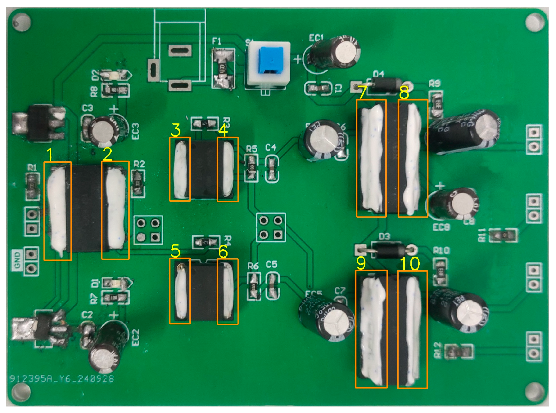
3.2. Region of Interest Extraction

The Region of Interest (ROI) is often obscured by extraneous backgrounds in captured images, which are regarded as noise during the image processing procedure. Consequently, the PCB region is extracted from the original image and transformed into a front-view image. The preprocessing stage involves the elimination of the background, the suppression of noise, and the initial extraction of features.
In color images, the green surface of PCBs exhibits a pronounced contrast with the background, whereas this difference is less evident in grayscale images. The edges of the PCB are extracted based on the Hue-Saturation-Value (HSV) space of color images. Figure 3 shows the PCB image segmentation workflow.
The image-processing stage employs a Gaussian smoothing filter, which effectively removes high-frequency noise while preserving more edge information. Pixel neighborhoods in edge regions usually vary significantly. Edge blurring will be reduced through the Gaussian filter’s weighted distribution method. Mean filtering reduces image noise through the holistic processing of images.
Compared with a grayscale image, there are significant differences between a PCB and its background in an HSV image, as shown in Figure 4.
The implementation of an HSV threshold segmentation method within the ROI is instrumental in facilitating the removal of the background while ensuring the preservation of the PCB edge features. This method exerts a filtering-like effect; thus, the corresponding operation can be designated as HSV filtering.
The algorithm can be expressed as follows:
r h = R   | h m i n h h m a x
where R represents the extracted ROI, hmax and hmin denote the upper and lower bounds of the HSV threshold, respectively. h represents the HSV value of each pixel in the HSV image. The PCB background color in the HSV image is predominantly green. In the HSV color space, the color green corresponds to the range of (42, 51, 59) to (85, 255, 255). The upper and lower bounds employed in this study are thus hmax (85, 255, 255) and hmin (42, 51, 59), respectively. The threshold ranges are subject to adjustment during the segmentation process, intending to attain optimal outcomes.
Figure 4c shows that the binary image has undergone HSV threshold filtering. However, the PCB image currently exhibits jagged edges following the removal of the background, as demonstrated in Figure 5. The edge-smoothing process is achieved through the utilization of bilateral filtering and convex hull detection algorithms. Bilateral filtering employs a combination of spatial proximity and pixel similarity to enhance image smoothness while preserving edge structure, a technique frequently employed in denoising and smoothing operations that maintain edge integrity. The algorithm process is illustrated in Figure 6.
Following the implementation of edge-smoothing processing, the resultant image is characterized by an enhanced representation of edge information, as illustrated in Figure 7. The edges are rendered with a smooth appearance, devoid of any discernible noise or jaggedness.
Hough line detection is used to extract the PCB image edges, as shown in Figure 8. The smoothed image edges do not constitute a straight line; rather, they are composed of multiple line segments that were spliced together. The endpoints of each line segment exhibit a robust linear correlation. An approximate PCB image edge can be obtained by linear fitting the points on each edge segment.
The endpoint information obtained from Hough line detection is stored in the same set, and it is necessary to first classify the endpoints. The following distance-based linear classification algorithm is proposed to classify endpoints into four categories, which can be expressed as follows:
p ( i ) = ( x i , y i ) ,   i = 1 , 2 , , n
where p(i) represents the set of endpoint coordinates, xi is the horizontal coordinate of endpoint i in the image coordinate system, yi is the vertical coordinate, and n represents the endpoint number.
The quadrilateral vertices A(xa, ya), B(xb, yb), C(xc, yc), and D(xd, yd) are defined here. The following equations are assumed:
x a = min ( { x i } ) ,   y a = min ( { y i } ) x b = max ( { x i } ) ,   y b = min ( { y i } ) x c = max ( { x i } ) ,   y c = max ( { y i } ) x d = min ( { x i } ) ,   y d = max ( { y i } ) ,   i = 1 , 2 , , n
where min (*) denotes the process of extracting the smallest value from the specified dataset. Conversely, max (*) is utilized to identify the largest value within the given dataset. {xi} is the horizontal coordinate set of the lowest point within the image coordinate system, while {yi} denotes the vertical coordinate set of the corresponding point.
The endpoints obtained by Hough line detection can be contained within the quadrilateral ABCD. Derivation of a general line equation is possible, which can then be used to obtain the line representations of each side of the quadrilateral.
A 1 x + B 1 y + C 1 = 0 A 2 x + B 2 y + C 2 = 0 A 3 x + B 3 y + C 3 = 0 A 4 x + B 4 y + C 4 = 0
where
A 1 = y b     y a B 1 = x a     x b C 1 = x b     y a     x a     y b ,   A 2 = y c     y b B 2 = x b     x c C 2 = x c     y b     x b     y c ,   A 3 = y d     y c B 3 = x c     x d C 3 = x d     y c     x c     y d ,   A 4 = y d     y a B 4 = x a     x d C 4 = x d     y a     x a     y d
In accordance with the distance equation from a point to a straight line, when combined with (2) and (4), the distance from each endpoint to each edge in the set can be calculated as follows:
L i , j = A i x j + B i y j + c i A i 2 + B i 2 ,   i = 1 , 2 , 3 , 4 j = 1 , 2 , , n
where Li,j is the distance from the endpoint j to the straight line i.
For any endpoint, its distance to each edge is as follows:
L i = A i x + B i y + c i A i 2 + B i 2 , i = 1 , 2 , 3 , 4
Let Pi(m) = {(xm, ym)}, i = 1, 2, 3, 4, m = 1, 2,…, m be an endpoint classification set. If the distance L from any endpoint (x, y) to the straight line li satisfies (7), then (x, y)∈Pi(m).
L = min ( L i ) , i = 1 , 2 , 3 , 4
where min(*) is used to denote the process of extracting the minimum value from the given set of inputs.
As demonstrated in Figure 9, four endpoint classification sets can be obtained from (2) to (7), with each endpoint set corresponding to an edge of the PCB image.
The Least Squares Method for line fitting can be employed to obtain the corresponding line for the specified endpoint set. The general equation can be expressed as follows:
A i x + B i y + C i = 0 ,   i = 1 , 2 , 3 , 4
Any line in (8) can be combined with its adjacent lines to obtain one intersection point:
P = { p i } ,   i = 1 , 2 , 3 , 4 p i = { ( u i , v i ) }
where (ui, vi) denotes the coordinate of the intersection point between the straight line i and the adjacent straight line in the image coordinate, pi is the coordinate of the intersection point i, and P is the coordinate set of all intersection points.
The approximate PCB edge can be obtained by connecting the four intersection points in sequence, as shown in Figure 10.
In the process of capturing images of PCBs, the PCB is not invariably positioned in a fixed orientation. It can thus be concluded that the size and rotation pose of the segmented PCB images are not entirely consistent. A perspective transformation algorithm is employed to convert the segmented PCB image to a fixed state, thereby facilitating standardized inspection.
The transformation of perspective is contingent upon the alignment of the perspective center, image point, and target point, which must be collinear. Subsequently, the viewing plane must undergo rotation around the trajectory by a specific angle, following the perspective rotation law. This process destroys the original projection beam whilst ensuring that the projection on the perspective plane remains unaltered. The fundamental principle underlying this process is to project the image onto a novel viewing plane. The general transformation equation is shown in (10):
x , y , z = u , v , w A A = a 11 a 12 a 13 a 21 a 22 a 23 a 31 a 32 a 33
where [u, v, w] is the pixel coordinate of the original image, [x′, y′, z′] is the pixel coordinates of the target image, and A is the perspective transformation matrix. The parameters w′ and w are generally set to 1 in a two-dimensional plane. Therefore, the preceding equation can be simplified as follows:
x , y , 1 = u , v , 1 a 11 a 12 a 13 a 21 a 22 a 23 a 31 a 32 1
According to the PCB design dimensions, the theoretical minimum envelope rectangle aspect ratio for the four installation circles is 19:14. Consequently, any image size at this ratio can be used for perspective transformation to restore the adhesive image in the front view. In this work, the image size is set to M(w, h) = (1900, 1400), and the vertex coordinates’ set of the target image P’ = {(0, 0), (1900, 0), (1900, 1400), (0, 1400)} can be obtained. The transformation matrix can be solved by combining (9) and (11). The substitution of each pixel coordinate in the PCB image into (11) will result in the transformation of the image, as shown in Figure 11.

3.3. Standard Template Establishment

Following the process of perspective transformation, the PCB board image is rendered in front view. The dimensions, positioning, and other properties of the image can be set to a fixed value. Subsequently, the adhesive region must be labeled and segmented, as shown in Figure 12. Each adhesive block is to be divided into a distinct image area (orange box). The dimensions of the image region are typically 1.1–1.5 times the size of the adhesive area. The following set S is employed to record the information of each image area.
S = s i   , i = 1 , 2 , , n s i = ( u 1 , i , v 1 , i ) , ( u 2 , i , v 2 , i ) , a i
where S is the set of adhesive regions. si is the information of adhesive region i. The coordinates of the upper left and lower right corners of adhesive region i are given by (u1,i, v1,i) and (u2,i, v2,i), respectively. ai is the area of adhesive region i. It is noted that the orange boxes illustrated in Figure 12 are manually defined at the current stage, and their size is set according to the dispensing experience.
Each adhesive region will undergo a series of processing steps, including background removal, filtering, and edge detection. The area of each adhesive block can be obtained, and the processing flow is shown in Figure 13a. To illustrate this process, the analysis is focused on block 1, with the results presented in Figure 13b. The application of mean filtering is instrumental in the reduction in noise before the transformation of the image into grayscale. Gaussian filtering is a process that suppresses noise to provide a low-noise input for subsequent edge detection algorithms. This, in turn, has the indirect effect of enhancing the accuracy of edge detection. Each adhesive block is processed through the algorithm in Figure 13a. The adhesive block area can be obtained as P = {pi}, I = 1, 2, …, n. The following standard template can then be established by combining (12):
T = t i   , i = 1 , 2 , , 26 t i = ( u 1 , i , v 1 , i ) , ( u 2 , i , v 2 , i ) , h i
where T is the standard template state set for adhesive blocks, ti is the standard adhesive state of adhesive block i, and hi is the standard area value of block i. A single template applies only to its corresponding PCB design. If another PCB wishes to be detected, it is necessary to redefine both the template and the orange boxes. During the manual operation process, incorrect drawing of these orange boxes means that the proposed template method cannot capture useful region information, resulting in a failed detection mission.

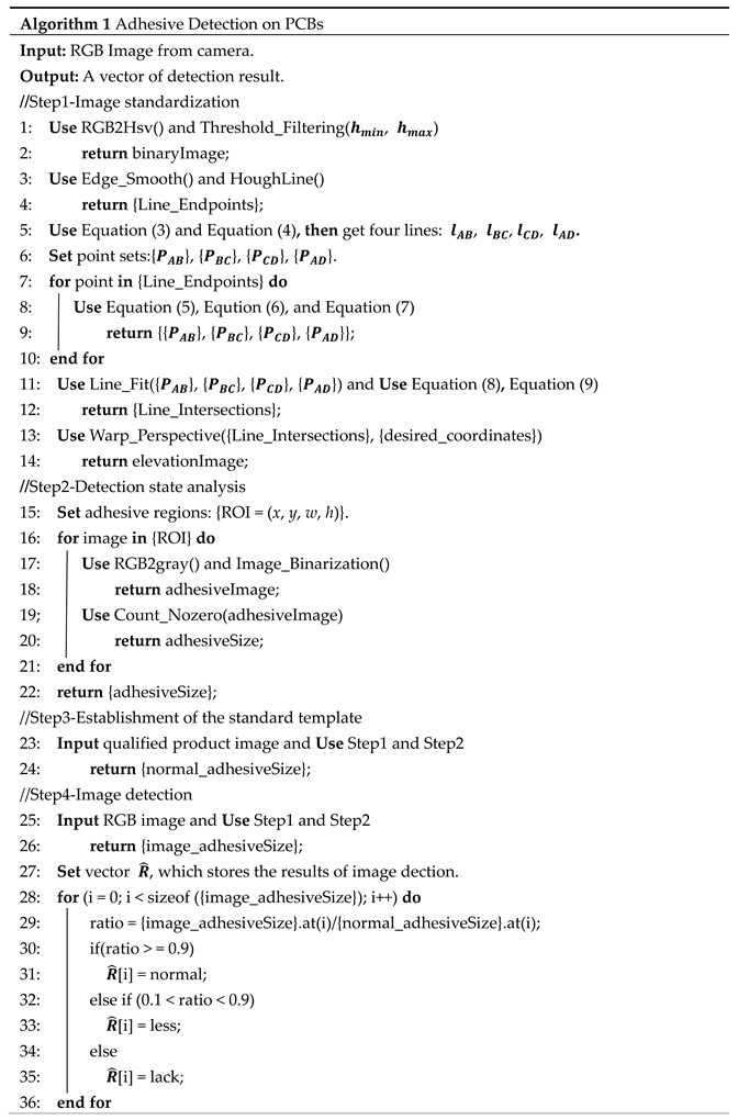
3.4. Detection Algorithm

The following presentation outlines the previously mentioned detection algorithm in pseudocode, as outlined in Algorithm 1. The inputs to the system are RGB images from a camera, and the outputs are the results of the detection process. The process comprises four distinct stages: Step 1 is image standardization, Step 2 is detection state analysis, Step 3 is the establishment of the standard template, and Step 4 is image detection. The detection result (normal, less, or lack) can be determined by the ratio parameter. At present, the ratio values are dependent on experience.
Electronics 14 02045 i001

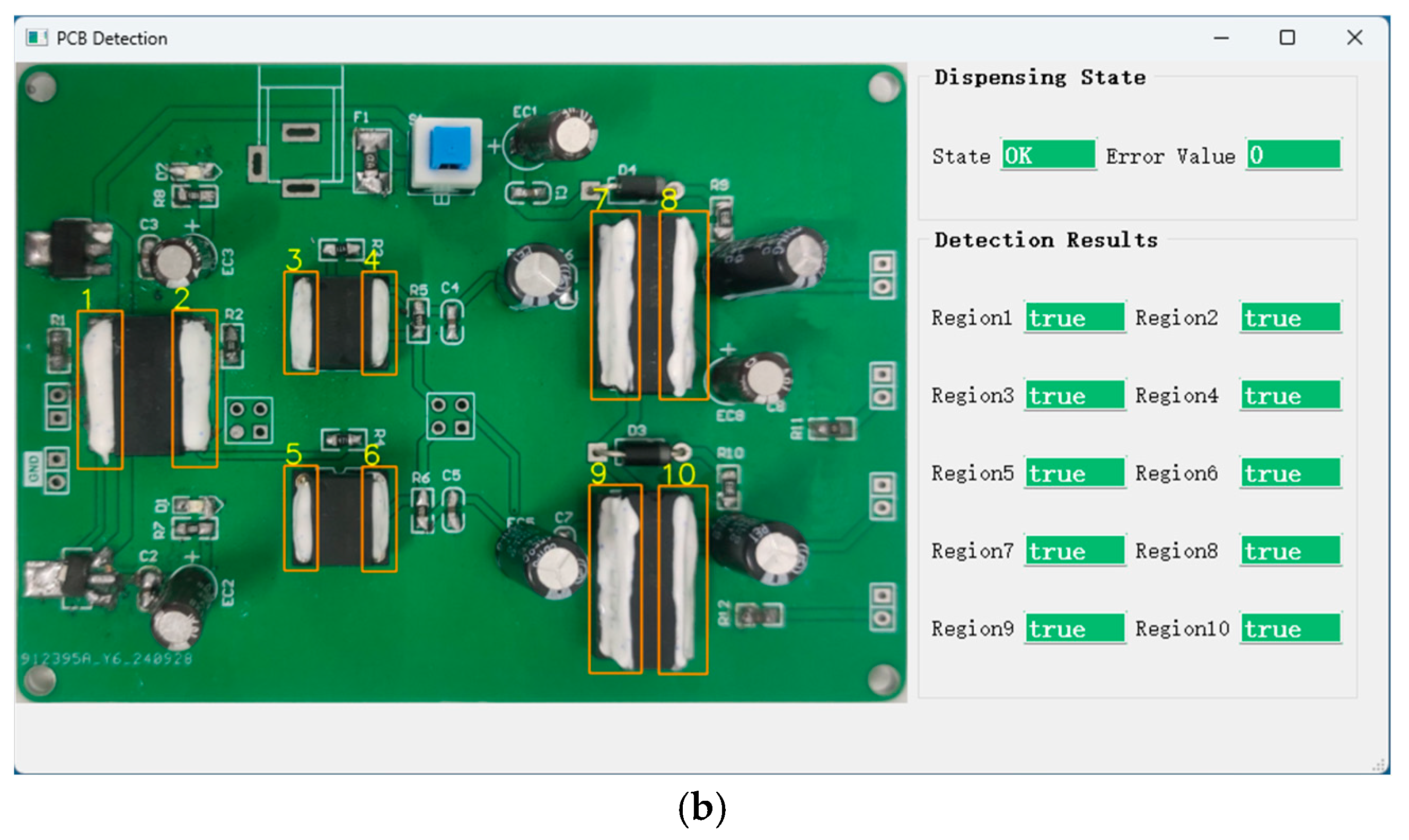
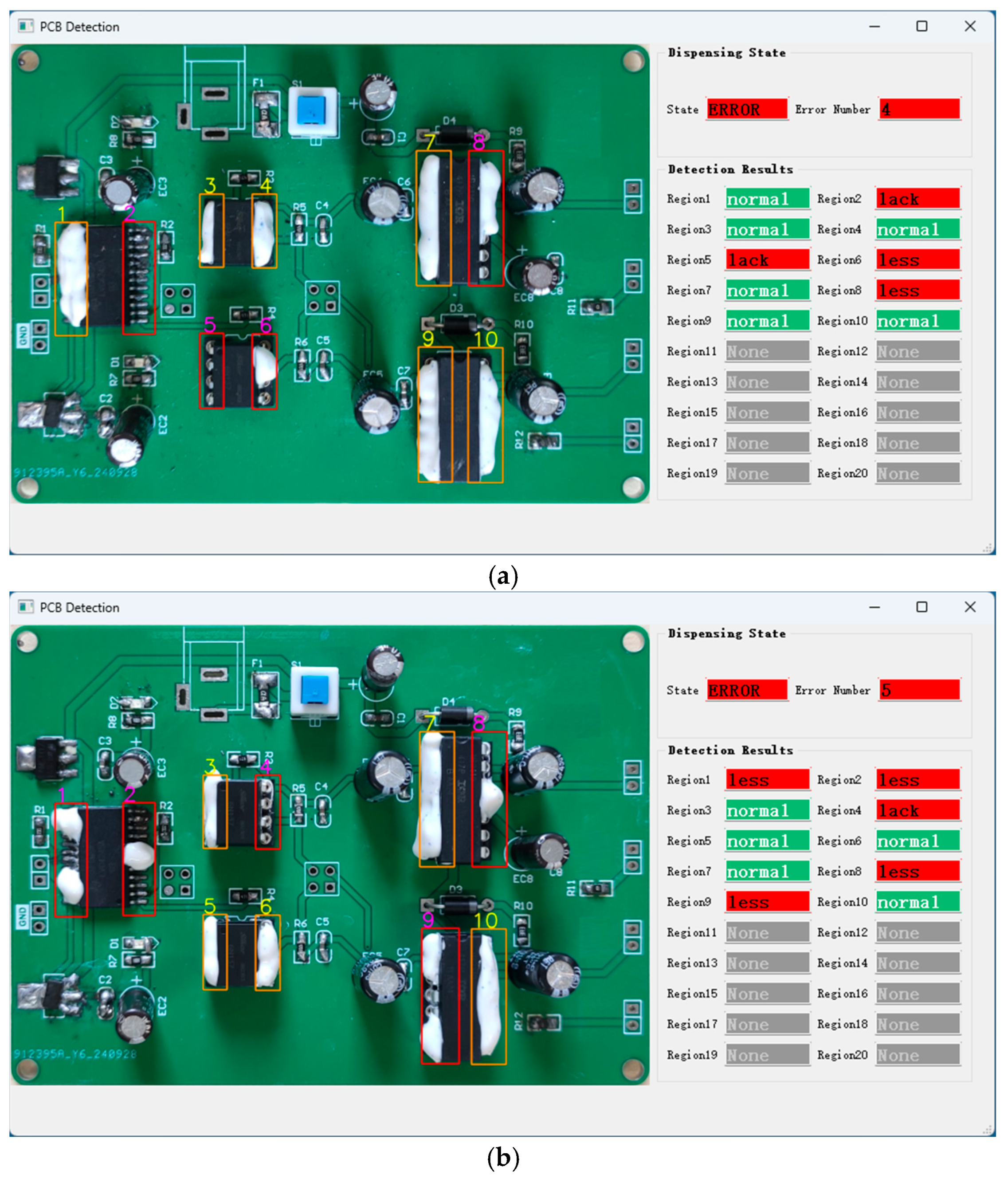
3.5. Detection Software

The development of an operation interaction software was undertaken to facilitate the detection of PCBs’ structural adhesives and to display the results. The software was based on Qt UI, the OpenCV library, and the C++ programming language. The configuration of the interface is delineated in Figure 14, which comprises an image display region situated on the left and a resulting state region positioned on the right. The second version of the software is capable of displaying 20 adhesive regions, and there are no initial states. Each region is characterized by three distinct status categories: normal, less, and lack. The categories delineated herein are indicative of the presence of adhesives that are either qualified, insufficient, or absent. The software operates on the Windows operating system, and its record log format is capable of being set as TXT or XLS.
The software’s workflow is shown in Figure 15. The initial stage is preparation, followed by image preprocessing. After the detection stage, post-processing encompasses data analysis, interface display, and result recording.

4. Experiment

4.1. Experimental Condition and Process

A series of structural adhesive detection tests is conducted to evaluate the efficacy of the present paper. The parameters of the processing hardware system are enumerated in Table 1. The camera establishes a connection between the NUC processor using a high-speed USB interface and subsequently captures images of the PCB under constant-lighting conditions. The detection process can be configured to operate in real-time or offline mode.
Two types of PCBs are used for detection tests, as shown in Table 2. The first PCB is distinguished by its green solder masks, with dimensions of 95 mm in length and 70 mm in width. By way of contrast, the second PCB features black solder masks, with a length of 85 mm and a width of 55 mm. A salient distinction between the two PCBs pertains to the number of adhesive regions; the green PCB possesses 10 adhesive regions, while the black PCB has 15. The software employed for this purpose was designed to detect these PCBs in distinct groups. A total of three experiments were conducted, and the ensuing results are displayed in the following section.
The experimental process is shown in Figure 16. After placing a PCB, the light source needs to be adjusted to capture clear images. The processing procedure is the image-processing stage, as depicted in Figure 15. The recording logs and detected image are output last.

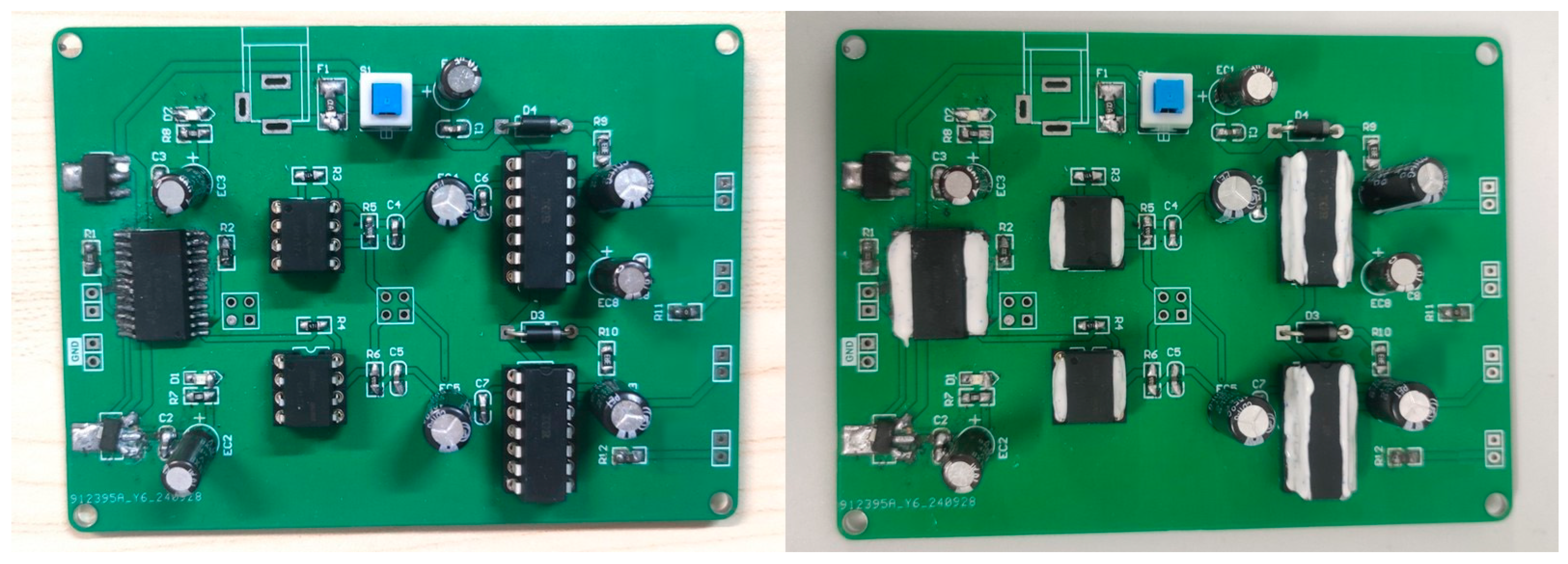
4.2. Detection of Absent and Insufficient Adhesives

The initial experiment is designed to detect the presence of adhesives that are either absent or insufficient on PCBs. Based on the first PCB design in Table 3, 6 PCBs are soldered for testing. White adhesives are then dispensed on various regions of the boards, with each region having a distinct volume and shape. The camera is employed to collect a total of 80 images, with each image depicting a distinct adhesive state on the 6 PCBs. The software then proceeds to automate the processing of these images, sequentially analyzing each one until all adhesive regions have been captured. The detection results are subsequently displayed on the software panel, with different versions indicating the outcomes.
  • Detection of Absent Adhesives
Figure 17 shows that the qualified adhesive areas are demarcated by orange rectangles, while the unqualified areas are indicated by red. These rectangles are displayed in accordance with the template. In the right part of the figure, the detection results indicate that the adhesive regions that meet the required standards are highlighted in green, while those that do not meet the required standards are marked in red. Figure 17a further illustrates three regions devoid of adhesive, which are denoted by the software with a red warning. The overall state of this PCB is designated as ERROR, as indicated by three error values, which, in turn, provide the respective numbers of adhesive regions. As illustrated in Figure 17b, all regions were dispensed with qualified adhesive. Consequently, the overall state is classified as satisfactory, as it exhibits no error.
In Figure 18a, two regions without adhesives are recorded by ‘lack’ (i.e., Region 2 and Region 5), while the regions exhibiting insufficient adhesive are denoted by ‘less’ (i.e., Region 6 and Region 8). It is noteworthy that these regions are unqualified and are indicated by the color red, thereby signifying an error state and an error value of 4. Similar experiments are shown in Figure 18b.
The log file documents the detection outcomes of Figure 17 and Figure 18. While the 80 test images are not sufficiently numerous when compared to other extant learning-based datasets, we make efforts to evaluate and analyze the proposed method under the existing conditions. For PCBs with qualified adhesive, the method may lead to over-detection, but there are no cases of missed detection, i.e., some qualified PCBs are treated as unqualified ones; the accuracy in this scenario is 95%. In actual applications, the over-detection judgement can be accepted as preferable to missed detection. The detection of absent adhesive can be readily accomplished through the utilization of a template-based method, which is inherently capable of achieving 100% accuracy. However, the accuracy of insufficient adhesive detection is notably lower, with an accuracy of 90%, when compared to other scenarios. The process operates at a speed of 60 frames per minute. The presence of minute volumes and shapes of adhesive poses challenges to vision-based detection. Two direct schemes can be applied to increase the accuracy of the detection process. The first is to select a camera with a higher resolution, and the second is to repeat the detection process several times. Other methods with high performance can also be studied to guarantee the accuracy of the detection process.

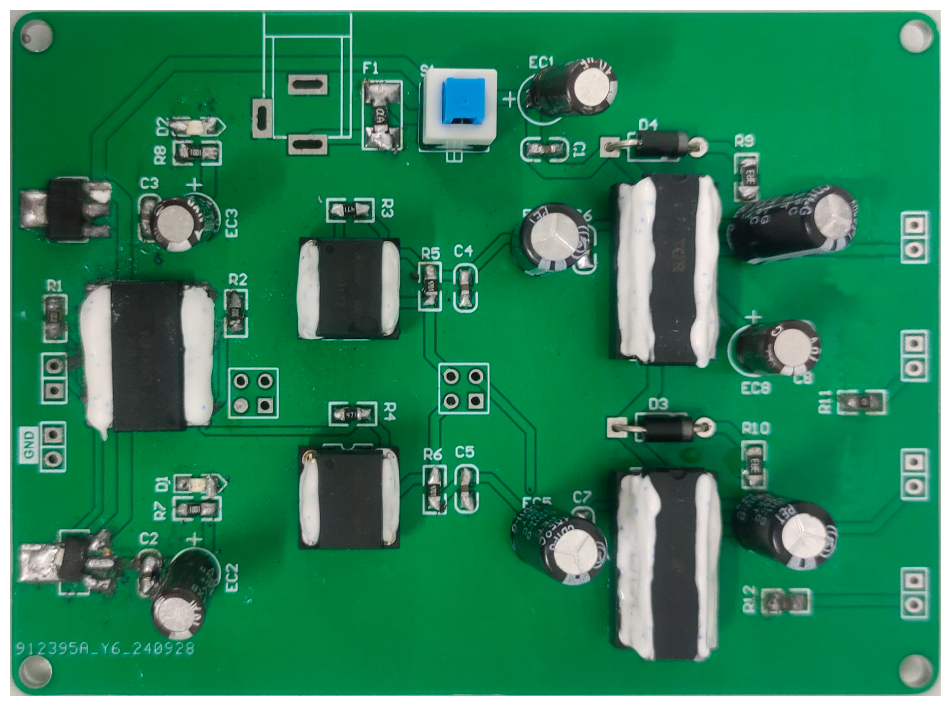
4.3. Detecting Adhesive on Different PCBs

A PCB with a black solder mask is used to test the method. By constructing a corresponding template, the adhesive detection result is shown in Figure 19 and Table 4.
Based on the second PCB design in Table 2, 4 PCBs are mounted, and 60 images are collected for tests. The software detects these images and displays the results. Table 4 shows the detection results. The small black PCBs are populated with smaller electronic components, which serve to make the adhesive more visible. It is necessary to calibrate the HSV filter to detect adhesive regions on the black background. As demonstrated in Table 4, the method can achieve a higher level of accuracy, albeit with a concomitant increase in over-detection. The adhesive detection accuracy is found to be 93% when using limited PCB image samples. The process speed is 60 frames per minute, which is suitable for online detection. According to the adhesive-dispensing process, the occurrence of over-detection can be accepted for qualified PCB production.

4.4. Experimental Summary

To summarize the experiments above, the following results can be obtained:
(1) The method was demonstrated to be effective in the detection of adhesive states on different PCBs within the designated hardware and software environment. The outcomes substantiate the efficacy and dependability of the proposed methodology.
(2) The over-detection problem is evident within the PCB detection process. On the one hand, the ineffectiveness of the adhesive can be identified; on the other hand, it guarantees no cases of missed detection.
(3) In the absence of open datasets, this work merely accumulates numerous images for evaluation experiments. A more substantial dataset of images pertaining to adhesive dispensing is required.

5. Conclusions

This paper studies the structural adhesive detection problem. The HSV segmentation method is employed to extract PCB regions from the original images, and the Hough Transform algorithm is subsequently applied to detect the morphology. Subsequently, the perspective transformation process involves the extraction and rectification of adhesive regions from the PCB images. The adhesive region template is constructed manually by detecting the standard adhesive area ratio in its corresponding adhesive region. Finally, the adhesive regions are detected using template matching, thereby enabling the automatic inspection of the PCB. This method has been demonstrated to possess the capability to accurately detect the adhesive state of PCBs and to identify locations that meet the required standards, thus providing an effective vision-based detection scheme within the electric industry.
However, there are several problems that need to be addressed in future study:
  • Poor generalization capability.
The current method depends on a template-matching idea. This means that one template is only applicable to a single type of PCB. Different PCBs have various layout designs and surface features. If the generalization problem is addressed within the conventional object detection methodology framework, two stages require attention. In the HSV segmentation stage, for a single image, the k-means clustering method can help segment different colors. In addition, different colored lights can shine on a PCB to collect multiple images, and the colors can be segmented based on the reflectance differences in the PCB surface. In the initial template establishment phase, the robustness of PCB detection can be enhanced through the substitution of static template matching with feature-based key-point methods. Enhancing the generalization capability of the method can be achieved through the implementation of improvements in these specific aspects.
  • Lacking sufficient automation and intelligence in the detection process.
The adhesive detection process depends too much on manual operations, e.g., filtering stage and ROI rectangular box, resulting in low efficiency. In recent years, deep-network-based methods have become increasingly prevalent in a variety of industrial detection scenarios. The YOLO series algorithms are a prime example and particularly effective in target detection tasks. To apply the YOLO network to adhesive detection tasks, two key issues must be addressed. Firstly, it is imperative to have a substantial dataset of adhesive-dispensing PCBs. A novel adhesive dataset can be constructed through the integration of existing datasets of PCB electronic components and local adhesive-dispensing images. Or the regular PCB component dataset can generate adhesive regions by learning various adhesive shapes. Secondly, rectangular boxes can be automatically drawn by adjustable candidate boxes, following the same principle as the anchor boxes in YOLO algorithms. Improving any of the above-mentioned issues will lead to a breakthrough in detection efficiency.
Although the present study offers limited methodological innovation in the field of adhesive detection, it addresses fundamental questions and conducts preliminary testing, thereby laying the groundwork for future methodologies.

Author Contributions

Conceptualization, R.Z. and T.Y.; methodology, R.Z.; software, T.Y.; validation, R.Z. and T.Y.; formal analysis, R.Z. and J.Z.; investigation, R.Z.; resources, J.Z.; data curation, T.Y.; writing—original draft preparation, R.Z.; writing—review and editing, R.Z. and T.Y.; visualization, T.Y.; supervision, J.Z.; project administration, J.Z.; funding acquisition, J.Z. All authors have read and agreed to the published version of the manuscript.

Funding

This research was funded by the Jiangsu Province Engineering Research Center of Integrated Circuit Reliability Technology and Testing System and the Wuxi Taihu Light Science and Technology Research Plan (Grant No. K20241049).

Data Availability Statement

Data supporting the results of this study are available from the corresponding author upon request.

Acknowledgments

The authors thank the engineers of Wuxi Tailianxin Technology Co., Ltd., for supporting PCB products and related technology.

Conflicts of Interest

Authors Ruzhou Zhang and Tengfei Yan were employed by the company Wuxi Tailianxin Technology Co., Ltd. The remaining authors declare that the research was conducted in the absence of any commercial or financial relationships that could be construed as a potential conflict of interest.

References

  1. Ren, G.; Tian, F.; Yang, L. The research of thermal design for vehicle controller based on simulation. Appl. Therm. Eng. 2013, 58, 420–429. [Google Scholar]
  2. Park, T.; Oh, H. New PCB strain-based structural design methodology for reliable and rapid evaluation of spaceborne electronics under random vibration. Int. J. Fatigue 2021, 146, 106147. [Google Scholar] [CrossRef]
  3. Liu, F.; Gong, R.; Duan, Z.; Wang, Z.; Zhou, J. Effect of PCB fastening method and thickness on PCB assembly vibration reliability in thermal environments. Microelectron. Reliab. 2025, 165, 115587. [Google Scholar] [CrossRef]
  4. Freitas, C.; Leite, T.; Lopes, H.; Gomes, M.; Cruz, S.; Magalhães, R.; Silva, A.F.; Viana, J.C.; Delgado, I. Influence of adhesive on optical fiber-based strain measurements on printed circuit boards. J. Mater. Sci. Mater. Electron. 2023, 34, 699. [Google Scholar] [CrossRef]
  5. Deng, W. Investigation of visual inspection methodologies for printed circuit board products. J. Opt. 2024, 53, 1462–1470. [Google Scholar] [CrossRef]
  6. Rahman, A.; Mousavi, A. A review and analysis of automatic optical inspection and quality monitoring methods in electronics industry. IEEE Access 2020, 8, 183192–183271. [Google Scholar]
  7. Sankar, V.; Lakshmi, G.; Sankar, Y. A review of various defects in PCB. J. Electron. Test. 2022, 38, 481–491. [Google Scholar] [CrossRef]
  8. Crispin, A.; Rankov, V. Automated inspection of PCB components using a genetic algorithm template-matching approach. Int. J. Adv. Manuf. Tech. 2007, 35, 293–300. [Google Scholar] [CrossRef]
  9. Ren, W.; Luo, J.; Jiang, W.; Qu, L.; Han, Z.; Tian, J.; Liu, H. Learning self-and cross-triplet context clues for human-object interaction detection. IEEE Trans. Circuits Syst. Video Technol. 2024, 34, 9760–9773. [Google Scholar] [CrossRef]
  10. Ulger, F.; Yuksel, S.E.; Yilmaz, A.; Gokcen, D. Solder joint inspection on printed circuit boards: A survey and a dataset. IEEE Trans. Instrum. Meas. 2023, 72, 2515121. [Google Scholar] [CrossRef]
  11. Wang, Q.; Huang, Z.; Fan, H.; Fu, S.; Tang, Y. Unsupervised person re-identification based on adaptive information supplementation and foreground enhancement. IET Image Process. 2024, 18, 4680–4694. [Google Scholar] [CrossRef]
  12. Song, X.; Wang, Y.; Li, C.; Song, L. WDC-YOLO: An improved YOLO model for small objects oriented printed circuit board defect detection. J. Electron. Imaging 2024, 33, 013051. [Google Scholar] [CrossRef]
  13. Zhang, J.; Shi, X.; Qu, D.; Xu, H.; Chang, Z. PCB defect recognition by image analysis using deep convolutional neural network. J. Electron. Test. 2024, 40, 657–667. [Google Scholar] [CrossRef]
  14. Liu, Z.; Qu, B. Machine vision based online detection of PCB defect. Microprocess. Microsyst. 2021, 82, 103807. [Google Scholar] [CrossRef]
  15. Gaidhane, V.H.; Hote, Y.V.; Singh, V. An efficient similarity measure approach for PCB surface defect detection. Pattern Anal. Appl. 2018, 21, 277–289. [Google Scholar] [CrossRef]
  16. Chen, Z.; Jiang, H.; Wang, Y.Q.; Jing, Y.Q. Research on machine vision-based alignment system in PCB inkjet printer. In Proceedings of the International Conference on Information Engineering and Applications (IEA); Springer: London, UK, 2012; pp. 689–697. [Google Scholar]
  17. Wang, W.B.; Liu, D.Y.; Yao, Y.Q. Defects detection of printed circuit board based on the machine vision method. Appl. Mech. Mater. 2014, 494, 785–788. [Google Scholar] [CrossRef]
  18. Luo, Z.D.; Lei, L.; Li, H.X. Rotation-angle-based principal feature extraction and optimization for PCB defect detection under uncertainties. IEEE Trans. Ind. Inform. 2024, 21, 932–939. [Google Scholar] [CrossRef]
  19. Vafeiadis, T.; Dimitriou, N.; Ioannidis, D.; Wotherspoon, T.; Tinker, G.; Tzovaras, D. A framework for inspection of dies attachment on PCB utilizing machine learning techniques. J. Manag. Anal. 2018, 5, 81–94. [Google Scholar] [CrossRef]
  20. Zhou, Y.; Yuan, M.; Zhang, J.; Ding, G.; Qin, S. Review of vision-based defect detection research and its perspectives for printed circuit board. J. Manuf. Syst. 2023, 70, 557–578. [Google Scholar] [CrossRef]
  21. Wang, W.C.; Chen, S.L.; Chen, L.B.; Chang, W.J. A machine vision-based automatic optical inspection system for measuring drilling quality of printed circuit boards. IEEE Access 2016, 5, 10817–10833. [Google Scholar] [CrossRef]
  22. Chen, X.; Wu, Y.; He, X.; Ming, W. A comprehensive review of deep learning-based PCB defect detection. IEEE Access 2023, 11, 139017–139038. [Google Scholar] [CrossRef]
  23. Ma, Y.; Yin, J.; Huang, F.; Li, Q. Surface defect inspection of industrial products with object detection deep networks: A systematic review. Artif. Intell. Rev. 2024, 57, 333. [Google Scholar] [CrossRef]
  24. Lv, S.; Ouyang, B.; Deng, Z.; Liang, T.; Jiang, S.; Zhang, K.; Chen, J.; Li, Z. A dataset for deep learning based detection of printed circuit board surface defect. Sci. Data 2024, 11, 811. [Google Scholar] [CrossRef]
  25. Huang, W.; Wei, P. A PCB Dataset for Defects Detection and Classification. arXiv 2019, arXiv:1901.08204. [Google Scholar]
  26. Li, Y.T.; Guo, J.I. A VGG-16 based faster RCNN model for PCB error inspection in industrial AOI applications. In Proceedings of the IEEE International Conference on Consumer Electronics-Taiwan (ICCE-TW), Taiwan, China, 19–21 May 2018; pp. 1–2. [Google Scholar]
  27. Lei, R.; Yan, D.; Wu, H.; Peng, Y. A precise convolutional neural network-based classification and pose prediction method for PCB component quality control. In Proceedings of the 14th International Conference on Electronics, Computers and Artificial Intelligence (ECAI), Bucharest, Romania, 30 June–1 July 2022; pp. 1–6. [Google Scholar]
  28. Yu, J.; Zhao, L.; Wang, Y.; Ge, Y. Defect detection of printed circuit board based on adaptive key-points localization network. Comput. Ind. Eng. 2024, 193, 110258. [Google Scholar] [CrossRef]
  29. Ling, Q.; Isa, N.A.M.; Asaari, M.S.M. SDD-Net: Soldering defect detection network for printed circuit boards. Neurocomputing 2024, 610, 128575. [Google Scholar] [CrossRef]
  30. Lu, J.; Lee, S.H. Real-time defect detection model in industrial environment based on lightweight deep learning network. Electronics 2023, 12, 4388. [Google Scholar] [CrossRef]
  31. Li, Y.T.; Kuo, P.; Guo, J.I. Automatic industry PCB board DIP process defect detection with deep ensemble method. In Proceedings of the IEEE 29th International Symposium on Industrial Electronics (ISIE), Delft, The Netherlands, 17–19 June 2020; pp. 453–459. [Google Scholar]
  32. Li, Y.T.; Kuo, P.; Guo, J.I. Automatic industry PCB board DIP process defect detection system based on deep ensemble self-adaption method. IEEE Trans. Compon. Packag. Manuf. Technol. 2020, 11, 312–323. [Google Scholar] [CrossRef]
  33. Gao, Y.; Zhang, R.; Yang, M.; Sabah, F. YOLOv8-TDD: An optimized YOLOv8 algorithm for targeted defect detection in printed circuit boards. J. Electron. Test. 2024, 40, 645–656. [Google Scholar]
  34. Kong, W.; Zhang, Z.; Zhang, T.; Wang, L.; Cheng, Z.-Y.; Zhou, M. SMC-YOLO: Surface defect detection of PCB based on multi-scale features and dual loss functions. IEEE Access 2024, 12, 137667–137682. [Google Scholar] [CrossRef]
  35. Yang, Y.; Kang, H. An enhanced detection method of PCB defect based on improved YOLOv7. Electronics 2023, 12, 2120. [Google Scholar] [CrossRef]
  36. Zhang, J.; Chang, Z.; Xu, H.; Qu, D.; Shi, X. Printed circuit board defect image recognition based on the multimodel fusion algorithm. J. Electron. Packag. 2024, 146, 021009. [Google Scholar] [CrossRef]
  37. Chen, W.; Meng, S.; Wang, X. Local and global context-enhanced lightweight CenterNet for PCB surface defect detection. Sensors 2024, 24, 4729. [Google Scholar] [CrossRef] [PubMed]
  38. Ding, R.; Zhang, C.; Zhu, Q.; Liu, H. Unknown defect detection for printed circuit board based on multi-scale deep similarity measure method. J. Eng. 2020, 13, 388–393. [Google Scholar] [CrossRef]
Figure 1. A PCB with and without structural adhesive. The left subfigure corresponds to the absence of adhesive, while the right subfigure corresponds to its presence.
Electronics 14 02045 g001
Figure 2. The structural adhesive detection process.
Electronics 14 02045 g002
Figure 3. The PCB image segmentation workflow.
Electronics 14 02045 g003
Figure 4. The PCB image processing results. (a) The grayscale image. (b) The HSV image. (c) The binary image.
Electronics 14 02045 g004
Figure 5. The enlarged detail of the jagged edge.
Electronics 14 02045 g005
Figure 6. The edge-smoothing algorithm process.
Electronics 14 02045 g006
Figure 7. The edge-smoothing PCB image.
Electronics 14 02045 g007
Figure 8. The result image of Hough line detection.
Electronics 14 02045 g008
Figure 9. The endpoint classification image.
Electronics 14 02045 g009
Figure 10. The PCB edge-fitting image.
Electronics 14 02045 g010
Figure 11. The PCB perspective transformation image.
Electronics 14 02045 g011
Figure 12. Image segmentation of each adhesive region.
Electronics 14 02045 g012
Figure 13. The adhesive block segmentation algorithm and the processing result. (a) The adhesive block segmentation algorithm process. (b) The processing result of adhesive block 1.
Electronics 14 02045 g013
Figure 14. The interface layout of detection software.
Electronics 14 02045 g014
Figure 15. The detection workflow of the developed software.
Electronics 14 02045 g015
Figure 16. The experimental process of PCB detection.
Electronics 14 02045 g016
Figure 17. The processing result of structural adhesive detection. (a) There exist several absent adhesive regions, and they are indicated by red color. (b) All the adhesive regions are qualified, and a green color indicates them.
Electronics 14 02045 g017aElectronics 14 02045 g017b
Figure 18. The detection result of structural adhesive on PCBs. (a) There exist 4 regions with absent and insufficient adhesives. (b) There exist 5 regions with absent and insufficient adhesives.
Electronics 14 02045 g018
Figure 19. The adhesive detection result on small PCBs. (a) There exist 2 regions with absent and insufficient adhesives. (b) There exist 6 regions with absent and insufficient adhesives.
Electronics 14 02045 g019
Table 1. The hardware system parameters.
ItemTypeParameter
Processing systemMini Intel NUCIntel Core i7-13700H,
16 G RAM, 512 G SSD
CameraRGB
industrial camera
Effective Pixels: 2592 (H) × 1944 (V), Pixel size: 1.4 µm × 1.4 µm,
Frame rate ≥ 30 FPS
Table 2. Two types of PCBs.
No.PCB typeSize
(mm)
Solder
Mask Color
Adhesive
Regions
Main IC
Package
1Electronics 14 02045 i002(L) 95
(W) 70
Green10DIP
2Electronics 14 02045 i003(L) 85
(W) 55
Black15QFP
Table 3. The detection results recording of the first PCB.
PCB
Type
Adhesive
State
Total
Number
Detection ResultsAccuracy
(%)
Speed
NormalMissedOver(F/min)
Qualified
PCB
Qualified 4038029560
Unqualified
PCB
Absent20200010060
Insufficient2018119060
Table 4. The detection results’ recording of the second PCB.
PCB
Type
Adhesive
State
Total
Number
Detection ResultsAccuracy
(%)
Speed
NormalMissedOver(F/min)
Qualified
PCB
Qualified 30300010060
Unqualified
PCB
Absent15150010060
Insufficient1514019360
Disclaimer/Publisher’s Note: The statements, opinions and data contained in all publications are solely those of the individual author(s) and contributor(s) and not of MDPI and/or the editor(s). MDPI and/or the editor(s) disclaim responsibility for any injury to people or property resulting from any ideas, methods, instructions or products referred to in the content.

