Article

Cache-Based Design of Spaceborne Solid-State Storage Systems

1
National Space Science Center, Chinese Academy of Sciences, Beijing 100190, China
2
University of Chinese Academy of Sciences, Beijing 100049, China
*
Author to whom correspondence should be addressed.
Electronics 2025, 14(10), 2041; https://doi.org/10.3390/electronics14102041
Submission received: 21 April 2025 / Revised: 11 May 2025 / Accepted: 16 May 2025 / Published: 17 May 2025
(This article belongs to the Special Issue Parallel and Distributed Computing for Emerging Applications)

Abstract

:
To address the current limitations of spaceborne solid-state storage systems that cannot effectively support the parallel storage of multiple high-speed data streams, the throughput bottleneck of NAND FLASH-based solid-state storage systems was analyzed in relation to the high-speed data input requirements of payloads. A four-stage pipeline operation and bus parallel expansion scheme was proposed to enhance the throughput. Additionally, to support the parallel storage of multichannel data and continuity of pipeline loading, the shortcomings of existing caching schemes were analyzed, leading to the design of a storage system based on Synchronous Dynamic Random Access Memory (SDRAM). Model simulations indicate that, under extreme conditions, the proposed scheme could continuously receive and cache multiple high-speed file data streams into the SDRAM. File data were dynamically written into FLASH based on the priority and status of each partition cache autonomously, without overflow during caching. The system eventually entered a regular dynamic balance scheduling state to achieve parallel reception, caching, and autonomous scheduling of storage for multiple high-speed payload data streams. The data throughput rate of the storage system can reach 4 Gbps, thus satisfying future requirements for multichannel high-speed payload data storage in spaceborne solid-state storage systems.

1. Introduction

The spaceborne solid-state storage system is a key component of the satellite platform [1] and serves as a data hub to support the implementation of satellite missions and data processing. NAND FLASH-based solid-state memory has a high storage density, nonvolatility, and other characteristics, and has become the mainstream method for spaceborne data storage [2,3]. The main function of the spaceborne solid-state storage system is to receive system engineering and application data from the Loongson 2K1000 CPU of the main control module computer unit, categorize and store them as needed, read them, and send them back to the computer unit upon receiving playback instruction. The system also handles instruction and state interactions with the computer unit.
With the rapid development of the space industry, the demand for satellite storage systems for space exploration missions has been increasing [4,5,6], characterized by mission diversification, data complexity, and real-time operation requirements [7,8]. The types and quantities of payloads carried by satellites are expanding, including high-precision observation devices such as synthetic aperture radars (SARs), multispectral imagers (MSIs), and hyperspectral imagers (HSIs) [9,10,11]. These devices generate exponentially increasing volumes of data, resulting in a significant increase in the throughput and storage capacity of spaceborne solid-state storage systems [12]. However, traditional spaceborne solid-state storage systems are struggling to satisfy these demands in terms of throughput rate and storage capacity, leading to serious challenges in handling large amounts of high-speed data, concurrent tasks, and large-capacity storage requirements [13,14].
Traditional spaceborne solid-state storage systems mostly use customized designs with independent data interfaces, storage capacities, and storage rates for different satellite missions. While initially effective, the rapid growth in the number of satellite missions has made it difficult for the traditional approach to adapt to the current R&D needs owing to long development cycles, low R&D efficiency, and poor reusability. For example, the storage system used in the dark matter particle detection satellite [15] had an effective throughput rate of approximately 350 Mbps, and only supported two-way data partition storage, making it unsuitable for high-speed input from multiple payloads, concurrent multitasking, and other modes of operation. Xu et al. [16] designed an image recording system based on FLASH, using CPU memory as a dual external image data cache. The CPU sequentially stores each cached image and then writes the data into the FLASH array, one by one. However, this cache scheduling approach restricts the input rate of the load data. Xu et al. [17] presents a design based on programmable nonvolatile memory by redivision of software functions and reselection of memory from the current status quo of the application of the spaceborne computer system in high orbit satellites. However, the application scenario of this work only considers the memory design issues related to the minimum system of the processor, which is not applicable in large-scale spaceborne solid-state memory design. Lv et al. [18] introduced a three-dimensional cross-mapping method based on double data rate (DDR)3 SDRAM to increase the memory access bandwidth and proposed an on-chip data transfer method based on superscalar pipelined buffers to improve the efficiency of data transfer; however, this method is not applicable to multichannel or multimode transmission scenarios. Zhu et al. [19] proposed an efficient and dynamically adaptive user-level direct memory access (uDMA) mechanism that can adapt to I/O requests for different data sizes and lighten the storage performance development kit (SPDK) v20.01 software stack by amortizing per-request latency. But it still does not address DMA’s dependence on the underlying hardware and potential data consistency issues. The application of data compression algorithms [20] in data caching can reduce actual storage requirements and effectively increase the available bandwidth. However, compression algorithms also introduce additional computational latency, and certain data types exhibit low compression ratios. Currently, in the field of space engineering, there is an urgent need for system-level research on spaceborne devices oriented towards high ingress rates and caching capabilities [21]. For example, in the work of Sun et al. [22,23], the Gaofen-5 remote sensing satellite carried six payloads with 27 operating modes, with the payload data transmission rate varying from 0.3 to 2.03 Gbps. These high data volumes and transmission rates create demand for high-speed data reception, and the multiple file types generated by multimode operation of the payloads need to be processed onboard, requiring high-speed data caching after reception. Therefore, it is necessary to develop a standardized and reliable high-speed caching system and interface.
This study focuses on the design requirements of spaceborne solid-state storage systems, identifies the bottleneck in throughput rate, and explores methods to improve it to support high-speed data reception and transmission. A cache-scheduling mechanism is designed and evaluated to address single-board memory demand for multiple high-speed data-synchronized caching and autonomous storage solutions. Finally, a system-level design of high-speed data reception and transmission on the order of Gbps, as well as file-by-file caching, is finally developed. In addition, under extreme conditions (characterized by continuous input of load data and the complete filling of each channel cache across all four clusters), the theoretical performance of the system is analyzed to provide a reference for system upgrades. After a series of experimental verifications, the results show that the data transmission attained sufficient speed and reliability, and that the system operates stably. This design provides important groundwork for the development of satellite-mounted solid-state storage systems.

2. Methodology

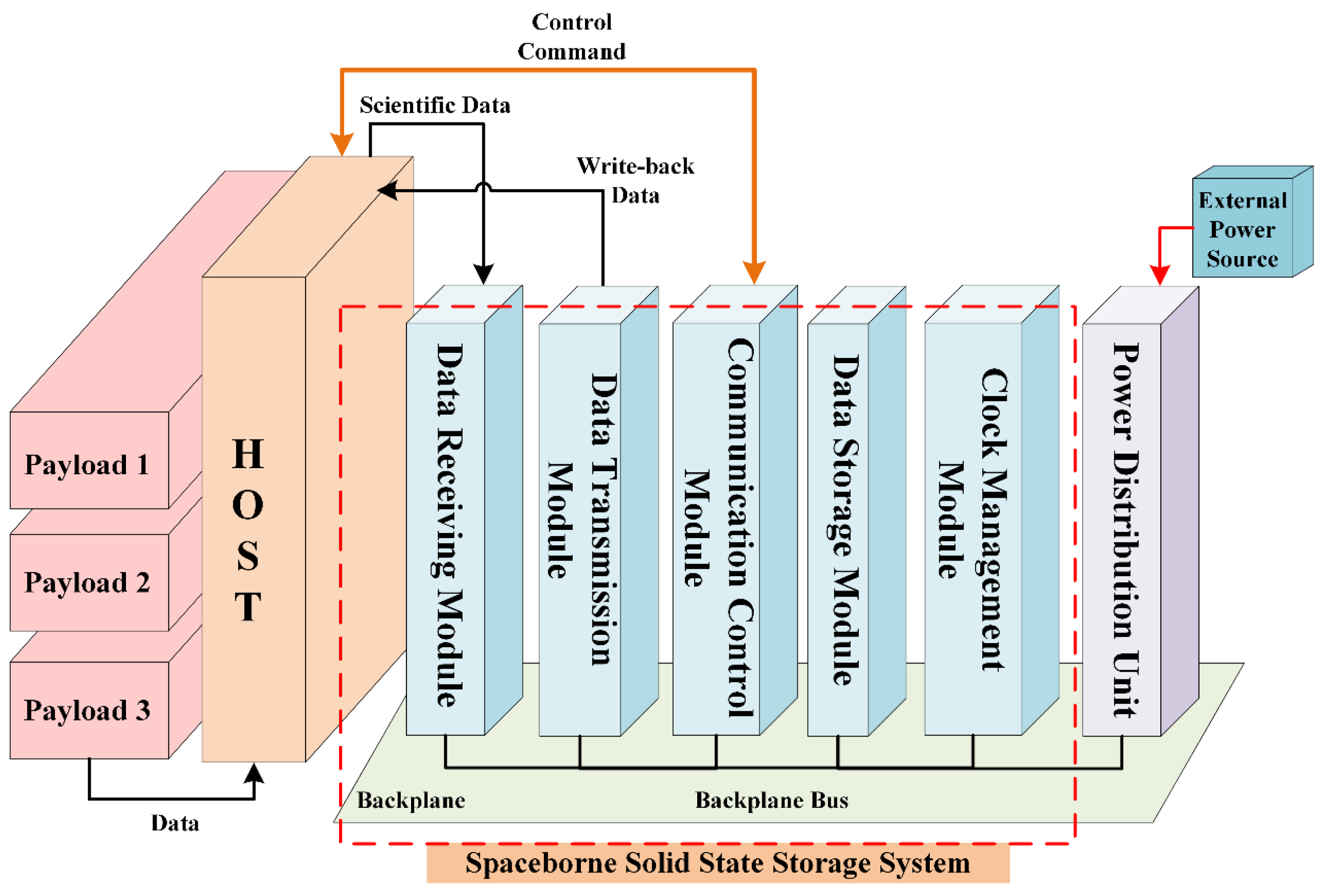
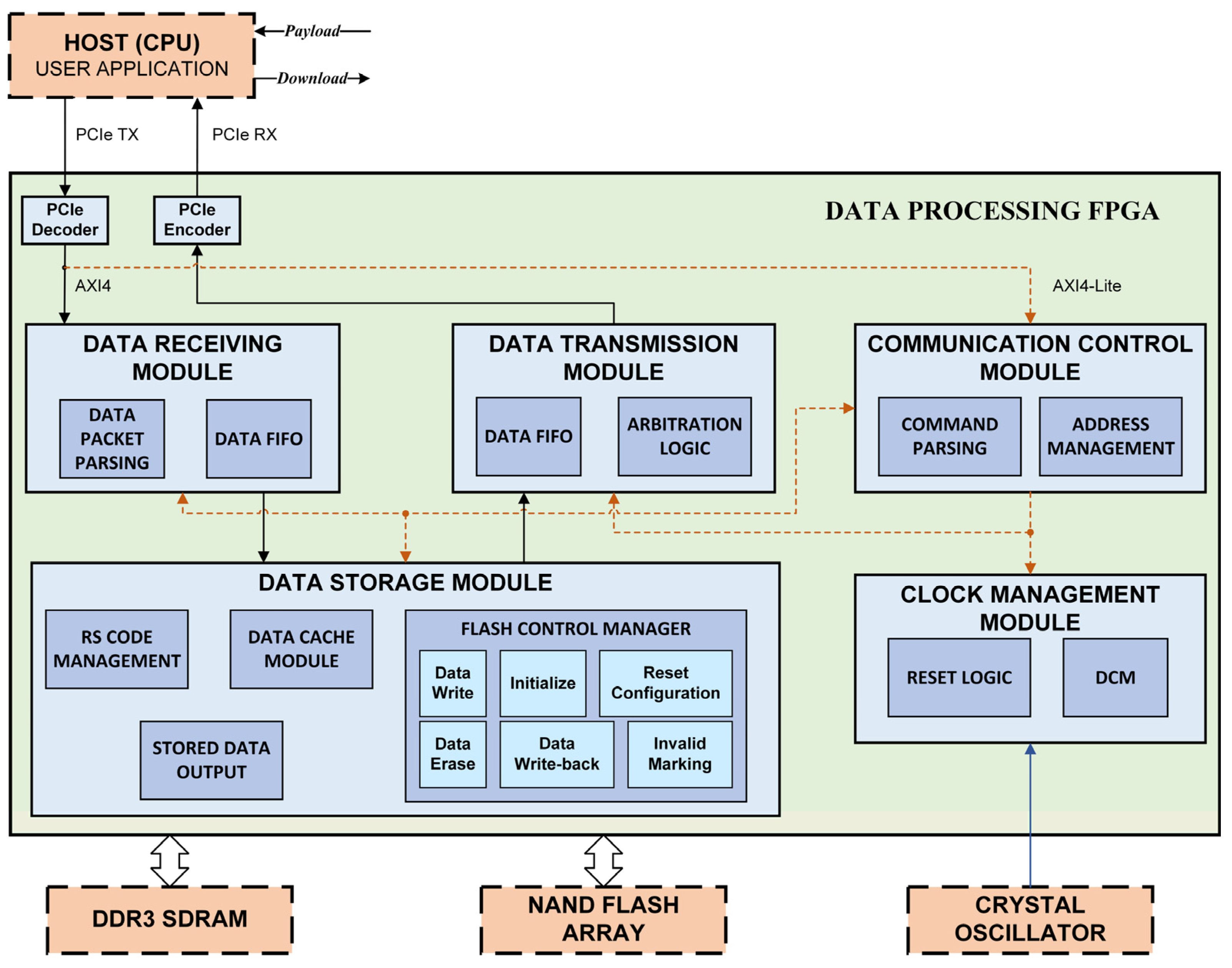
2.1. Overall Architecture

In order to solve the key technical problems of onboard data transmission and storage, and to meet the flexibility and reliability requirements of the spaceborne solid-state storage system, this paper proposes a highly modular, standardized, generalized, and highly reliable architecture of the onboard solid-state storage system; a composition and the surroundings of the system are shown in Figure 1.
The design idea of this architecture is to split the functions of the spaceborne solid-state storage system into independent functional modules, divide and define the functions, interfaces, and interrelationships of each module, and then interconnect the functional modules through a standard high-speed bus, transferring data between different functional modules through the high-speed bus.
The spaceborne solid-state storage system mainly consists of a data-receiving module, a data-sending module, a communication control module, a data-storage module, a clock management module, and a power distribution unit; the external interfaces of the system include a data input interface, a control command interface, a data output interface, and primary power interface.

2.2. Storage System Functional Module Design

Figure 2 shows the functional structure diagram of the spaceborne solid-state storage system, in which the black solid line part is the data flow, and the orange dashed line part is the control flow.
The specific functions of each component module are described below.
The data-receiving module receives the engineering data and application data sent by the CPU software of the external master control module.
The data-storage module receives the data parsed by the data-receiving module and stores them in the corresponding partition of the storage array according to the category.
The data transmission module plays back the time-delayed data in the data-storage module according to the instructions of the CPU software and sends them to the host.
The communication control module communicates with the CPU via a high-speed bus to accomplish storage control and status feedback.
The clock management module takes the external input clock and generates different frequency clocks needed by field programmable gate array (FPGA) from the digital clock manager (DCM) and generates the global reset signal.
The spaceborne storage scheme uses an FPGA as a controller carrier and an SDRAM high-speed parallel cache to store load data dynamically and independently in NAND FLASH. The CPU unit of the digital management system runs storage management software to complete information interaction work, such as storage unit task scheduling and storage block allocation, and implements file management of the storage system. The high-speed data from the payload is firstly transmitted to the data processing unit through the HOST (CPU) unit, where the FPGA completes the data format analysis and processing; then, according to the file type, the data are cached in the external cache chip DDR3; the cached data are composed into transmission frames when the satellite enters into the country. The data are sent to a downlinking unit through the HOST (CPU) unit to complete the inter-satellite data transmission. Thus, inter-satellite data transmission is completed.

3. Results and Discussion

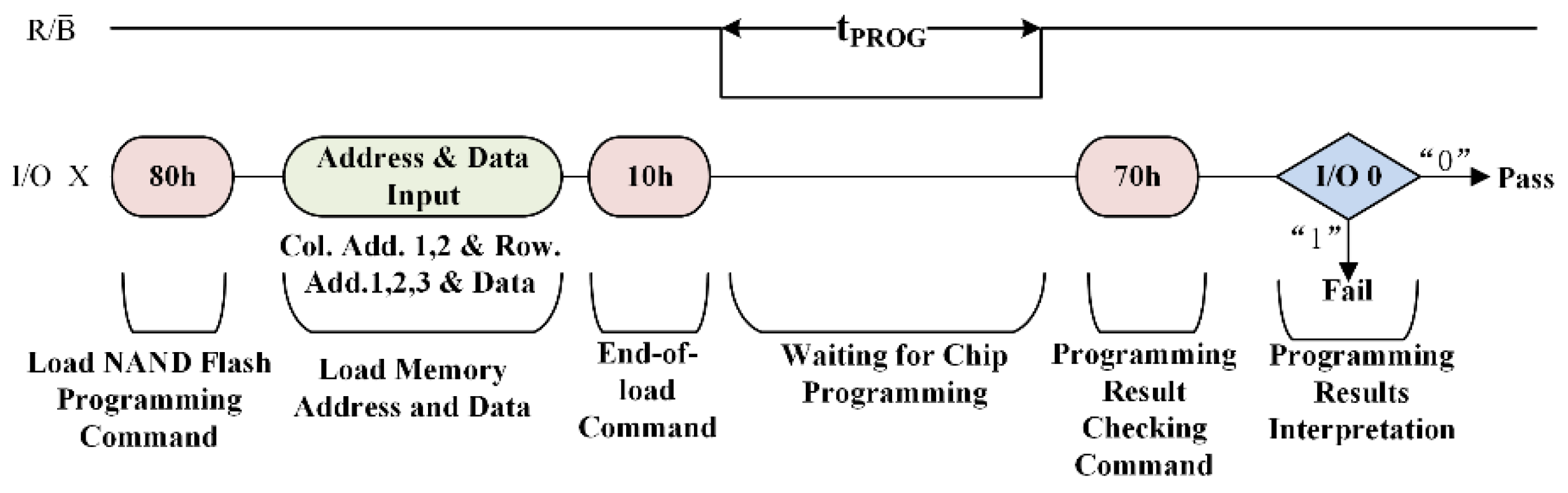
3.1. Analysis of Storage System Throughput Rate Constraints

Currently, satellite-mounted solid-state storage systems predominantly utilize space-grade NAND FLASH-stacked chips that have undergone anti-radiation hardening processes. When considering the FLASH data bus bitwidth of the stack module to be W o n e _ d i e , the maximum operating frequency is f f l a s h _ w o r k _ m a x , and the theoretical maximum throughput of a single module is
H o n e _ d i e _ t h e o r y _ m a x = f f l a s h _ w o r k _ m a x × W o n e _ d i e .
The SLC NAND FLASH chip used in the project is MT29F256G08AUCAB [24], which operated at 50 MHz during the experiment. Considering the military component derating standard [25], the practical maximum operating frequency for the NAND FLASH is consequently 32 MHz. According to Equation (1), the theoretical maximum throughput rate of the FLASH-stacked module is 256 Mbps.
The inherent characteristics of write operations in solid-state storage devices reduce their throughput. NAND FLASH substrates perform read and write operations per page. During data writing, the data are first loaded into the internal cache of the chip; then, the programming process completes the data writing process. The writing process is illustrated in Figure 3.
According to the write time sequence requirements, the time required to complete a page of data writing is as follows:
t p a g e _ p r o g r a m = t L O A D + t P R O G + t C H E C K ;
t L O A D = t C M D _ 80 h + t A d d r e s s + t A D L + t D A T A + t C M D _ 10 h + t C M D _ 70 h
The timing parameters are listed in Table 1, where t C L K is the clock cycle and N p a g e is the page capacity.
If the FLASH write efficiency is set to η o n e _ d i e _ p r o g r a m , and the maximum write rate is set to H o n e _ d i e _ w o r k _ m a x ,
η o n e _ d i e _ p r o g r a m = t C L K × N p a g e t p a g e _ p r o g r a m ,   a n d
H o n e _ d i e _ w o r k _ m a x = H o n e _ d i e _ t h e o r y _ m a x × η o n e _ d i e _ p r o g r a m .
According to Equations (2)–(5), the highest effective write efficiency of FLASH in actual operation is 44.72% and the highest write rate is 114.48 Mbps, which are insufficient for meeting the storage requirements of multichannel, high-speed load data and restricts the throughput performance of solid-state memory.

3.2. Methods to Improve System Throughput

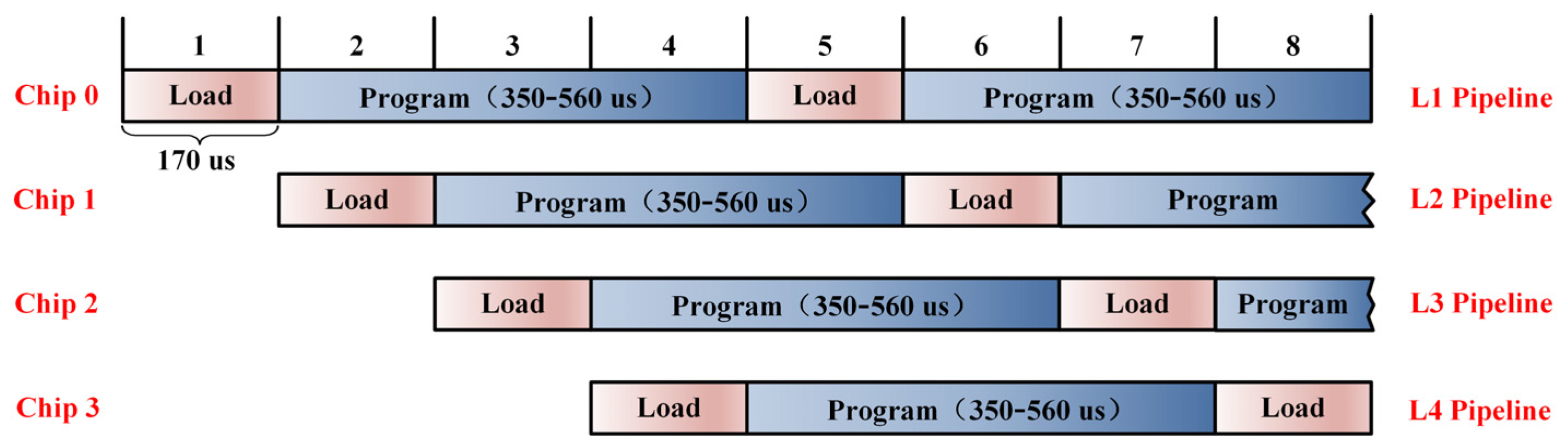
3.2.1. Pipeline Operation

In a FLASH write operation, chip programming takes a long time, which significantly reduces the write efficiency. This can be alleviated by pipelined operations. The principle of the pipeline FLASH write operation is illustrated in Figure 4.
Through the loading and programming of the pipeline, the four chips are guaranteed to complete continuous data writing in rotation, ensuring uninterrupted full-rate operation at the macro level. Thus, the effective FLASH write operation rate approaches the theoretical value of 256 Mbps, overcoming the limitations imposed by the inherent write operation characteristics of the storage medium on the effective throughput of the memory.

3.2.2. Bus Parallel Expansion Technology

The introduction of pipelined operations along the longitudinal time axis improves effective memory throughput; however, this improvement remains limited. To further improve the data processing rate and expand storage capacity, I/O bus parallel expansion technology was adopted along the horizontal space axis. Considering the FPGA pin resources and memory performance requirements, a parallel expansion scheme for a 16 × I/O bus was designed. The parallel expansion structure is shown in Figure 5.
To further increase the data processing rate and expand the storage capacity, the I/O bus parallel expansion and storage-depth expansion techniques were used. A 16 × I/O bus parallel expansion program was designed, with a bus width extended to 128 bits. The parallel pages in the NAND FLASH array were grouped into clusters for read and program operations.
Because the physical space expansion is independent of the chip operation timing, the system speed increased to 16 times after the 16 × bus expansion. Therefore, the memory board can theoretically support up to 4 Gbps of data input, improving the throughput capacity of the storage system for high-speed data load, and effectively meeting the requirements of most scientific satellite missions.

3.2.3. Caching Scheme Design

A multichannel, data-parallel receiving and caching mechanism was designed, as shown in Figure 6. Under conditions of multiple high-speed load data inputs in parallel, the combined unit sets the first in first out (FIFO) to receive the cache and sets the file number corresponding to it. The data are then sent to the storage control unit, where they are encoded by the Reed–Solomon (RS) (256,252) error correction, and then ping–pong cached via dual FIFO. When any FIFO cache reaches 256 words, it sends a read request to the SDRAM control module which sends data to the corresponding partition channel for caching according to the load data file number. When the amount of data cached in the SDRAM partition meets the requirements of the four-level pipeline (i.e., at least four clusters), the storage control FPGA and CPU unit cooperate to manage, initiate the FLASH write operation, and write the data into the solid-state storage media according to the four-level pipeline.

3.2.4. Channel Cache Scheduling and Storage Algorithm

Owing to the difference in the data rates of each load channel, the amount of cached data in each SDRAM partition is different. When multiple cache channels are full of four clusters simultaneously, or there are multiple four-cluster caches in one cache channel, the channel cache task scheduling mechanism ensures that the data are stored completely and effectively.
The FLASH write operation is given the highest priority, followed by the read operation and then the erase operation, ensuring that the FLASH load data are preferentially stored under complex working conditions. The system is designed to preferentially write FLASH to load data at a high rate in the SDRAM channel cache to prevent data cache overflow. The scheduling and storage flows of the channel cache tasks are shown in Algorithm 1.
The SDRAM control module polls the data cache of each channel according to the file number, from large to small. When the cache data of a channel comprise more than four clusters, the file number of the channel is stored. After all the channels are traversed, the current channel to be processed is determined. If more than four clusters of data exist in the operated cache channel, the four clusters are read according to the cache time sequence.
Algorithm 1: Channel cache scheduling and storage algorithm.
  Input:
  ● Cache channel data transfer rates: v1, v2, …, vn.
  ● Data buffer status for each cache channel: s1, s2, …, sn.
  ● NAND FLASH working status (WAIT, PROGRAM, WRITE_BACK, ERASE).
  ● Minimum pipeline threshold K.

  Output: NAND FLASH data scheduling strategy.
1Initialize: Create a queue for each cache channel (vi, si).
2 Sort all cache channels by data transfer rates vi in descending order, then assign file numbers fi (i = 1,2,…,n).
3for i = n downto 1 do // Poll cache channels from largest to smallest file number.
4   if NAND_Flash.state == FREE then
5     if SiK then
6       Choose cache channel i firstly with the highest data transfer rate.
7       Store file number fi, read data within the channel in FIFO order.
8       Buffer the data to NAND FLASH.
9       return scheduling strategy: PROGRAM scheduling.

10      else if NAND_Flash.state == WRITE_BACK then
11        Perform data playback operation.
12        return scheduling strategy: WRITE_BACK scheduling.
13
14      else if NAND_Flash.state == ERASE then
15        Perform data erase operation.
16        return scheduling strategy: ERASE scheduling.

17    else
18      Monitor NAND_Flash.state until NAND_Flash.state = FREE.
19      return scheduling strategy: WAIT scheduling.
20    end if
21End
The cache space required for each SDRAM channel is determined by the multichannel payload data rate. The condition to ensure that the channel cache does not overflow is that each SDRAM channel still has cache space when the memory is working under extreme conditions. In other words, when each SDRAM cache channel approaches the capacity of four clusters, NAND FLASH starts the erase operation. After the erase operation is completed, all the channel cache data are completely written to the FLASH storage area.

3.2.5. Algorithm Complexity Analysis

Time Complexity Analysis
Initialization and Sorting Phase:
Step 1: Initializing n queues incurs a time complexity of O (n).
Step 2: Sorting cache channels by transmission rates using optimal algorithms (e.g., quicksort/mergesort) requires O (n log n) time.
Cyclic Polling Phase:
Step 3: Iterates through all n cache channels, starting from the maximum file number. Each iteration involves: constant-time conditional checks (Steps 4–18): O (1) per operation.
Worst-case: All channels satisfy si < K with persistent FREE NAND status, requiring full traversal: O (n).
Best-case: Immediate satisfaction at the first channel (si ≥ K): O (1).
Total Time Complexity:
Dominated by the sorting phase’s O (n log n) term, yielding an overall time complexity of O (n log n).
Space Complexity Analysis
Data Structure Storage:
Step 1: Queue creation per channel: O (n).
Step 2: Sorting auxiliary space (e.g., mergesort): O (n).
Operational Overhead:
All other operations (status evaluation, strategy selection) use constant space: O (1)
Total Space Complexity:
Combined O (n) from dominant storage components.

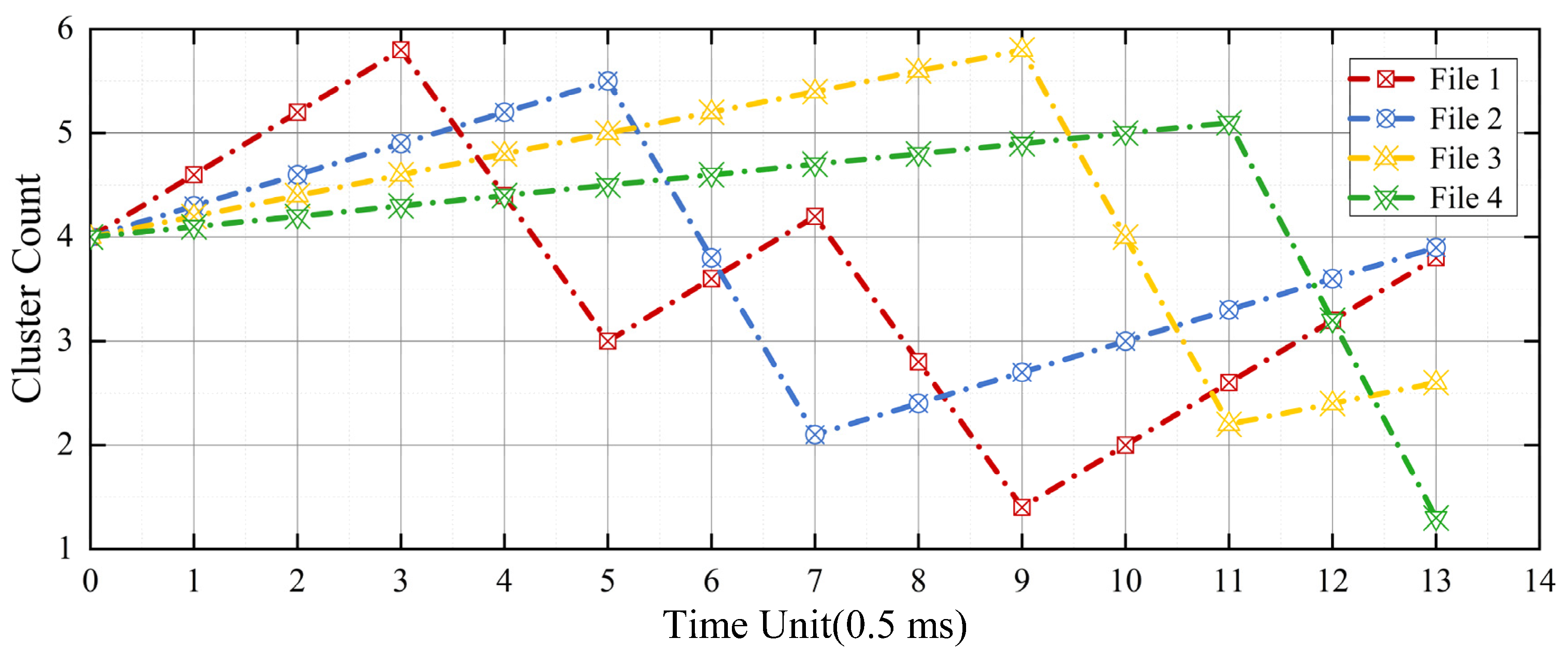
3.3. Simulation Validation

To evaluate the accuracy of the high-speed memory parallel cache design and task scheduling mechanism, the MATLAB (2019.a) software was used for model simulation. The input criteria were set as follows:
  • Four-way load with a data rate of 1.2 Gbps, 600 Mbps, 400 Mbps, and 200 Mbps;
  • Setting of file number from 1 to 4;
  • Continuous input of load data;
  • FLASH erase time of 1.5 ms, and 1 ms pipeline write of 4 data clusters;
  • No storage failure.
The changes in each file cache inside the SDRAM were simulated and observed; the results are shown in Figure 7.
When t = 0, all four file caches were composed of four clusters. As the erase task was blocked, FLASH did not perform write operations.
When t = 0–3, FLASH was erased, and the four files were continuously written to the SDRAM cache. No FLASH operation was performed.
When t = 3, the FLASH erasing ends. Each of the four file caches contained more than four clusters. The files were read according to priorities.
When t = 4, file 1 write was completed; files 2, 3, and 4 cache exceeded four clusters; file 2 cache was read and FLASH write was performed.
When t = 5, file 1 write was completed; files 2, 3, and 4 cache exceeded four clusters; file 2 cache was read and FLASH write was performed.
When t = 7, file 2 was completed, while files 1, 3, and 4 cache exceeded four clusters; file 1 was then read and FLASH write was performed.
When t = 9, file 1 write was completed, and the caches of files 3 and 4 are exceeded four clusters; file 3 then began reading FLASH.
When t = 11, file 3 operation was completed, and file 4 cache exceeded four clusters; file 4 reading was then initiated and FLASH write was performed.
When t = 13, the file 4 write operations were completed, and all cache files accumulated owing to the erase block were written into FLASH; the SDRAM then entered the normal dynamic balance scheduling state.
The utilization rates of each file cache within the SDRAM were simulated and monitored from time 0 to time 13; the results are shown in Figure 8.
As shown from the above figures, it is clear that each file cache channel leaves more than 40% redundant space, proving the rationality of the cache mechanism design. The average cache occupancies for files 1 to 4 are 25.82%, 34.61%, 43%, and 46.91%.
In summary, under extreme working conditions, the four channels of file data were continuously and concurrently received and cached into SDRAM and then dynamically and autonomously scheduled and written into FLASH according to the storage priority. The cache did not overflow and the entered system reached a normal dynamic balance scheduling state. The simulation results are in accordance with the design of the parallel cache and task scheduling mechanism and simultaneously meet the requirements of multichannel high-speed data input, showing that the scheme mechanism design was effective and feasible.
In recent years, numerous research institutions have devoted significant effort to the development of solid-state storage technology. Table 2 summarizes the performance of several spaceborne solid-state storage systems.
It is evident that the scheme proposed in this paper demonstrates substantial performance advantages.

4. Conclusions

To address the limitation of current spaceborne solid-state storage systems in supporting multichannel high-speed data storage, a four-stage pipelined operation and bus parallel expansion scheme were adopted to improve the storage capability and performance. An SDRAM high-speed multichannel caching and coordinated storage scheduling mechanism was designed to enable effective parallel cache reception and storage of multichannel data and to ensure the integrity of data storage under complex working conditions. The model and prototype function simulation results demonstrated that the design of the SDRAM high-speed multichannel cache and storage write co-scheduling mechanism was effective and reliable. In the future, we will consider designing a parallel storage architecture solution for multiple storage boards, realizing the management of multiple storage boards by one CPU to save resources and costs.

Author Contributions

Conceptualization, J.A.; data curation, C.L. and Z.D.; formal analysis, Q.Y.; methodology, C.L. and J.A.; writing—original draft, C.L.; writing—review and editing, J.A. and Z.D.; visualization, Q.Y.; supervision, C.L. and J.A.; project administration, J.A. and C.L. All authors have read and agreed to the published version of the manuscript.

Funding

This research was funded by the National Key R&D Program of China (2022YFF0503900).

Data Availability Statement

The data can be shared up on request.

Conflicts of Interest

The authors declare no conflicts of interest.

Abbreviations

The following abbreviations are used in this manuscript:
SDRAMSynchronous Dynamic Random Access Memory
SARsynthetic aperture radar
MSImultispectral imager
HSIhyperspectral imager
DDRdouble data rate
DMAdirect memory access
SPDKstorage performance development kit
FPGAfield programmable gate array
DCMdigital clock manager
FIFOFirst in first out
RSReed–Solomon

References

  1. Tu, S.L.; Wang, H.Q.; Huang, Y.; Jin, Z.H. A spaceborne advanced storage system for remote sensing microsatellites. Front. Inf. Technol. Electron. Eng. 2024, 25, 600–615. [Google Scholar] [CrossRef]
  2. Gong, Y.; Wang, Q.; Su, J. Efficient Management of FLASH Based Satellite Borne Storage. Microcomput. Inf. 2010, 26, 151. [Google Scholar]
  3. Luo, P.; Zhang, T. Data management of satellite-borne storage based on Flash. Appl. Res. Comput. 2018, 35, 479–482. [Google Scholar]
  4. Aourra, K.; Zhang, Q.X. An Energy Aware Mass Memory unit for small satellites using Hybrid Architecture. In Proceedings of the 20th IEEE International Conference on Computational Science and Engineering (CSE)/15th IEEE/IFIP International Conference on Embedded and Ubiquitous Computing (EUC), Guangzhou, China, 21–24 July 2017; pp. 210–213. [Google Scholar]
  5. Xie, Y.; Xie, Y.Z.; Li, B.Y.; Chen, H. Advancements in Spaceborne Synthetic Aperture Radar Imaging with System-on-Chip Architecture and System Fault-Tolerant Technology. Remote Sens. 2023, 15, 4739. [Google Scholar] [CrossRef]
  6. Jemmali, M.; Boulila, W.; Cherif, A.; Driss, M. Efficient Storage Approach for Big Data Analytics: An Iterative-Probabilistic Method for Dynamic Resource Allocation of Big Satellite Images. IEEE Access 2023, 11, 91526–91538. [Google Scholar] [CrossRef]
  7. Wang, C.L.; Yin, L.; Shen, X.H.; Dong, Z.; Ke, L. Design and Implementation of Spaceborne Fast Router Based on SDRAM. In Proceedings of the IEEE 11th International Conference on Communication Software and Networks (ICCSN), Chongqing, China, 12–15 June 2019; pp. 452–457. [Google Scholar]
  8. Wang, G.Q.; Chen, H.; Xie, Y.Z. An Efficient Dual-Channel Data Storage and Access Method for Spaceborne Synthetic Aperture Radar Real-Time Processing. Electronics 2021, 10, 622. [Google Scholar] [CrossRef]
  9. Shi, X.J.; Zhang, Y.H.; Dong, X. Evaluation of BAQ on Tiangong-2 Interferometric Imaging Radar Altimeter Data Compression. In Proceedings of the 22nd International Microwave and Radar Conference (MIKON), Poznan, Poland, 14–17 May 2018; pp. 623–624. [Google Scholar]
  10. Xiao, X.; Li, C.J.; Lei, Y.J. A Lightweight Self-Supervised Representation Learning Algorithm for Scene Classification in Spaceborne SAR and Optical Images. Remote Sens. 2022, 14, 2956. [Google Scholar] [CrossRef]
  11. Vitolo, P.; Fasolino, A.; Liguori, R.; Di Benedetto, L.; Rubino, A.; Licciardo, G.D. Real-Time On-board Satellite Cloud Cover Detection Hardware Architecture using Spaceborne Remote Sensing Imagery. In Proceedings of the Conference on Real-Time Processing of Image, Depth, and Video Information, Strasbourg, France, 8–9 April 2024. [Google Scholar]
  12. Wang, S.; Zhang, S.; Huang, X.; Chang, L. Single-chip multi-processing architecture for spaceborne SAR imaging and intelligent processing. J. Northwestern Polytech. Univ. 2021, 39, 510–520. [Google Scholar] [CrossRef]
  13. Martone, M.; Gollin, N.; Rizzoli, P.; Krieger, G. Performance-Optimized Quantization for SAR and InSAR Applications. IEEE Trans. Geosci. Remote Sens. 2022, 60, 22. [Google Scholar] [CrossRef]
  14. Gollin, N.; Martone, M.; Villano, M.; Rizzoli, P.; Krieger, G. Predictive Quantization for Onboard Data Reduction in Future SAR Systems. In Proceedings of the 13th European Conference on Synthetic Aperture Radar (EUSAR), Electr Network. 29 March–1 April 2021; pp. 570–575. [Google Scholar]
  15. Wang, L.; Zhu, Y.; Shen, W.; Liang, Y.; Teng, X.; Zhou, C. Centralized Payload Management System for Dark Matter Particle Explorer Satellite. Chin. J. Space Sci. 2018, 38, 567–574. [Google Scholar] [CrossRef]
  16. Xu, Y.; Ren, G.; Wu, Q.; Zhang, F. Key technology of invalid block management in NAND flash-based image recorder system. Infrared Laser Eng. 2012, 41, 1101–1106. [Google Scholar]
  17. Xu, N.; Li, Z.Y.; Wang, Z.Q.; Han, X.D.; An, W.Y.; Wang, X.Y.; Feng, Y.J. Optimization design and realization of GEO satellite onboard computer. Chin. Space Sci. Technol. 2020, 40, 94–100. [Google Scholar] [CrossRef]
  18. Lv, H.S.; Li, Y.R.; Xie, Y.Z.; Qiao, T.T. An Efficient On-Chip Data Storage and Exchange Engine for Spaceborne SAR System. Remote Sens. 2023, 15, 2885. [Google Scholar] [CrossRef]
  19. Zhu, J.B.; Wang, L.; Xiao, L.M.; Qin, G.J. uDMA: An Efficient User-Level DMA for NVMe SSDs. Appl. Sci. 2023, 13, 960. [Google Scholar] [CrossRef]
  20. Ketshabetswe, K.L.; Zungeru, A.M.; Mtengi, B.; Lebekwe, C.K.; Prabaharan, S.R.S. Data Compression Algorithms for Wireless Sensor Networks: A Review and Comparison. IEEE Access 2021, 9, 136872–136891. [Google Scholar] [CrossRef]
  21. Zhao, Y.; Chi, C.; Zhou, M.; Zheng, Y.; Sun, L.; Wang, X.; Zhang, J. A High Performance Solid State Storage Technology for Massive Data with High Transmission Bandwidth. Spacecr. Eng. 2020, 29, 162–168. [Google Scholar]
  22. Sun, Y.; Jiang, G.; Li, Y.; Yang, Y.; Dai, H.; He, J.; Ye, Q.; Cao, Q.; Dong, C.; Zhao, S.; et al. GF-5 Satellite: Overview and Application Prospects. Spacecr. Recovery Remote Sens. 2018, 39, 1–13. [Google Scholar]
  23. Chen, L.F.; Letu, H.; Fan, M.; Shang, H.Z.; Tao, J.H.; Wu, L.X.; Zhang, Y.; Yu, C.; Gu, J.B.; Zhang, N.; et al. An Introduction to the Chinese High-Resolution Earth Observation System: Gaofen-1∼7 Civilian Satellites. Remote Sens. 2022, 2022, 14. [Google Scholar] [CrossRef]
  24. Micron Technology, Inc. MT29F256G08AUCAB: 256Gb, 3V, 8-Bit, NAND Flash Memory Data Sheet. Available online: https://www.micron.com (accessed on 3 February 2025).
  25. GJB/Z 35-93; Derating Criteria for Electronic Components. Commission of Science, Technology and Industry for National Defense: Beijing, China, 1993.
  26. Earth Observation Satellite Missions and Sensors. Available online: https://directory.eoportal.org/ (accessed on 6 May 2025).
Figure 1. Components of spaceborne solid-state storage system.
Electronics 14 02041 g001
Figure 2. Functional modules of the spaceborne solid-state storage system.
Electronics 14 02041 g002
Figure 3. Timing diagram of the program operation of NAND FLASH.
Electronics 14 02041 g003
Figure 4. Flowchart of 4−level pipeline writing operation (The red color indicates the command loading phase of the chip, while the blue color denotes the programming phase).
Electronics 14 02041 g004
Figure 5. Diagram: 16 × FLASH I/O parallel expansion architecture.
Electronics 14 02041 g005
Figure 6. Flowchart of multichannel data parallel receiving and caching.
Electronics 14 02041 g006
Figure 7. Simulation of file parallel caching and storage scheduling models.
Electronics 14 02041 g007
Figure 8. Simulation of each file cache utilization rate.
Electronics 14 02041 g008
Table 1. FLASH programming operation timing parameter table.
ArgumentInstructionsTime
t C M D _ 80 h = t C M D _ 10 h = t C M D _ 70 h   Command loading time t C L K
t A d d r e s s Address loading time 5 × t C L K
t A D L Address to data load interval 70   ns
t D A T A Data loading time N p a g e × t C L K
t P R O G Programming latency350–560 μs
t C H E C K Programming results check time t W H R   |   t C L K
Table 2. Table of selected performance parameters for solid-state storage systems [26].
MissonStorage MediumCapacityStorage Rate
Sentinel-2NAND FLASH2400 Gb2 × 540 Mbps
CSGSDRAM1530 Gb2400 Mbps
SJ-10NAND FLASH256 Gb512 Mbps
ASO-SNAND FLASH4 Tb800 Mbps
CAS EarthNAND FLASH8 Tb2.6 Gbps
This WorkNAND FLASH8 Tb4 Gbps
Disclaimer/Publisher’s Note: The statements, opinions and data contained in all publications are solely those of the individual author(s) and contributor(s) and not of MDPI and/or the editor(s). MDPI and/or the editor(s) disclaim responsibility for any injury to people or property resulting from any ideas, methods, instructions or products referred to in the content.

