


A 0.6 V 68.2 dB 0.42 µW SAR-ΣΔ ADC for ASIC Chip in 0.18 µm CMOS


Abstract
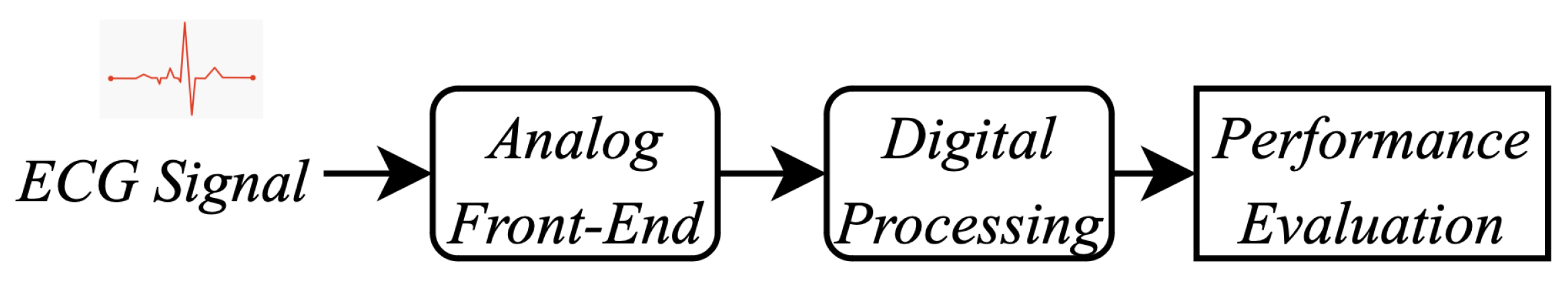
1. Introduction
- (1)
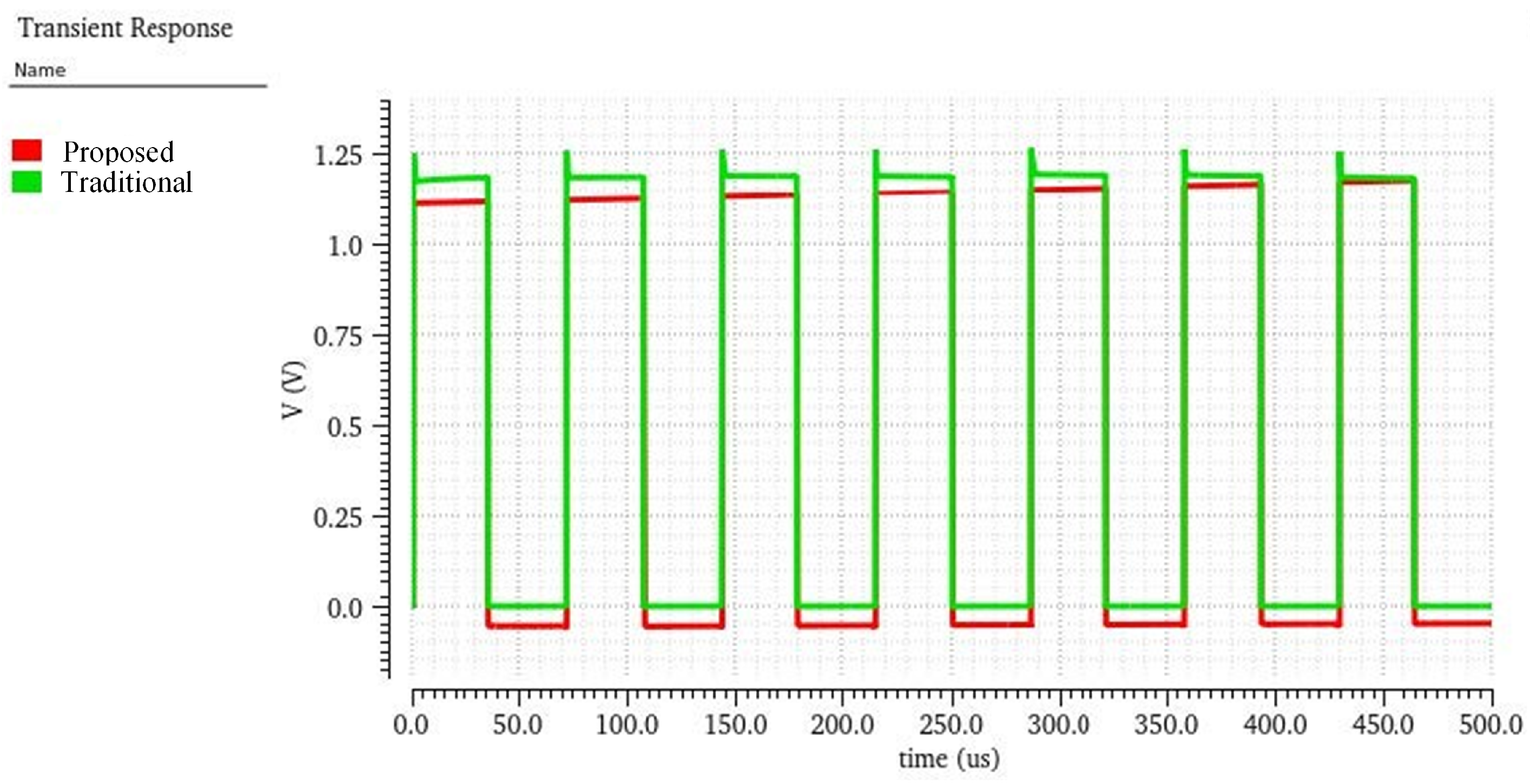
- A thorough analysis of the ISDM non-linear effect: First, the kickback noise of the voltage-controlled delay line (VCDL) was analyzed, which caused the VCM shift at the differential input of the ISDM stage. Then, the impact of PVT variations and VCM-induced shifts on the non-linearity of the ISDM stage was thoroughly investigated. Since the ISDM stage was highly sensitive to VCM shifts, this paper further proposes a modified merged capacitor switching (MCS) scheme to maintain a constant VCM during the conversion process, thereby mitigating non-linearity degradation.
- (2)
- A 13-bit hybrid bottom-plate sampling ADC architecture: The design first employed the presented bootstrap switches for bottom-plate sampling to reduce the leakage current. A 10-bit SAR ADC with the MCS scheme was then introduced to maintain the differential output of the VCDL at a constant common-mode level, thereby mitigating non-linearity and eliminating the need for a dedicated VCM voltage. This was followed by a 4-bit conversion performed by the ISDM ADC, including 1 redundant bit, resulting in an overall resolution of 13 bits.
- (3)
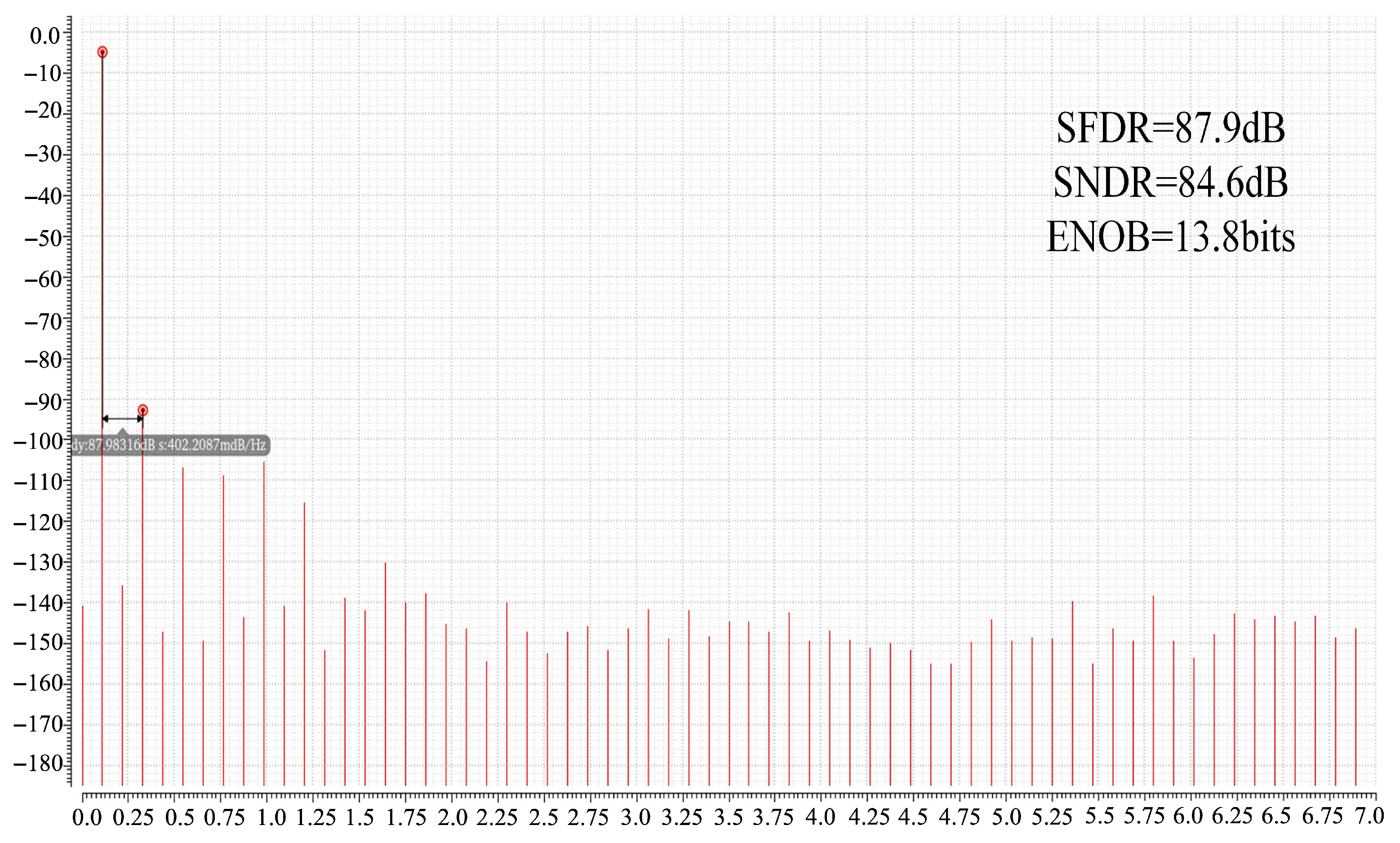
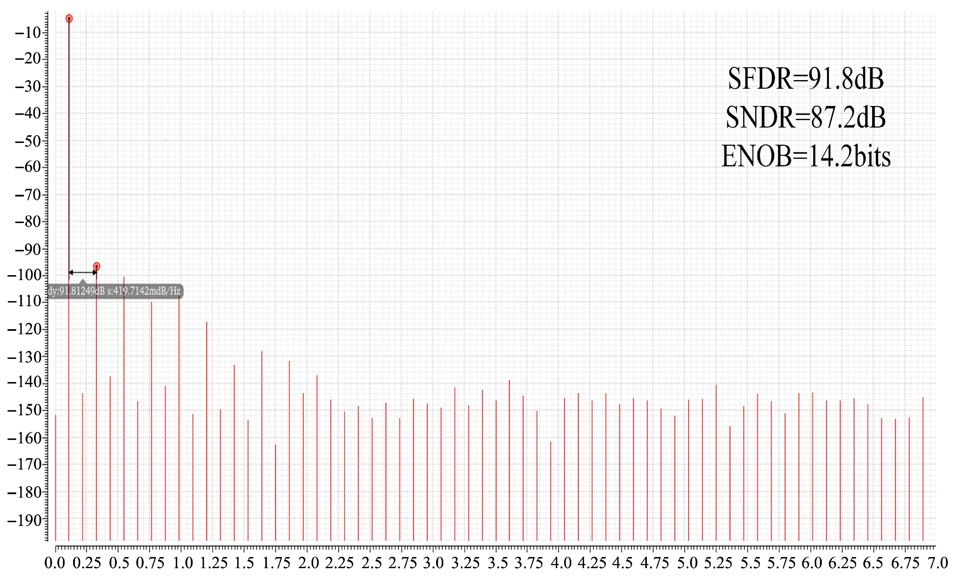
- Solid testing result of the low-power-consumption ADC: The chip testing results indicate that the circuit consumed a minimum power of 0.42 µW at a sampling rate of 10 kHz, with a supply voltage of 0.6 V. These findings demonstrate the robustness of our circuit. With a core area of 0.21 mm2 in 0.18 µm CMOS technology, the SNDR was measured at 68.2 dB, and the FOMw of 20.05 fJ/conversion-step was the lowest reported for ADCs of this architecture in a 0.18 µm process.
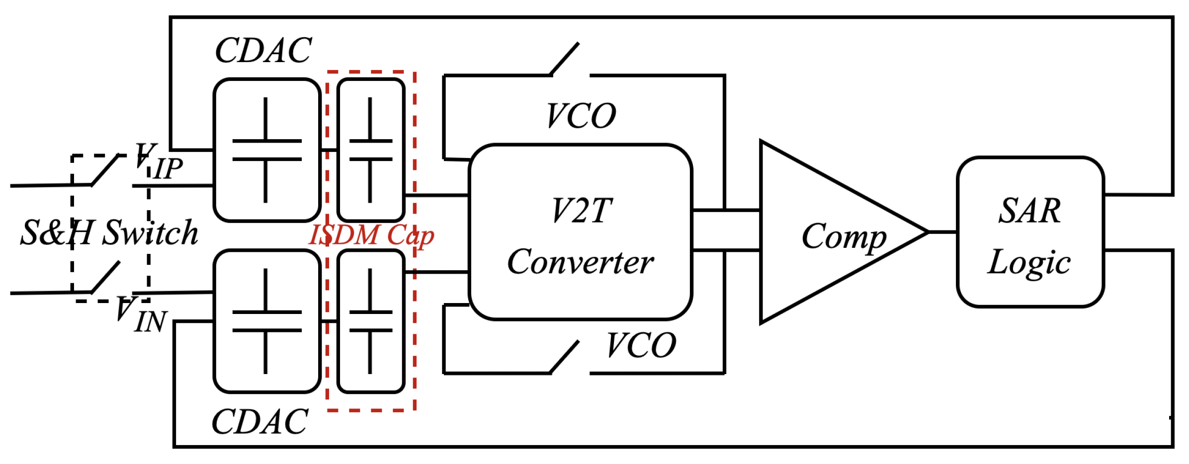
2. Architecture Review of the SAR–ISDM ADC
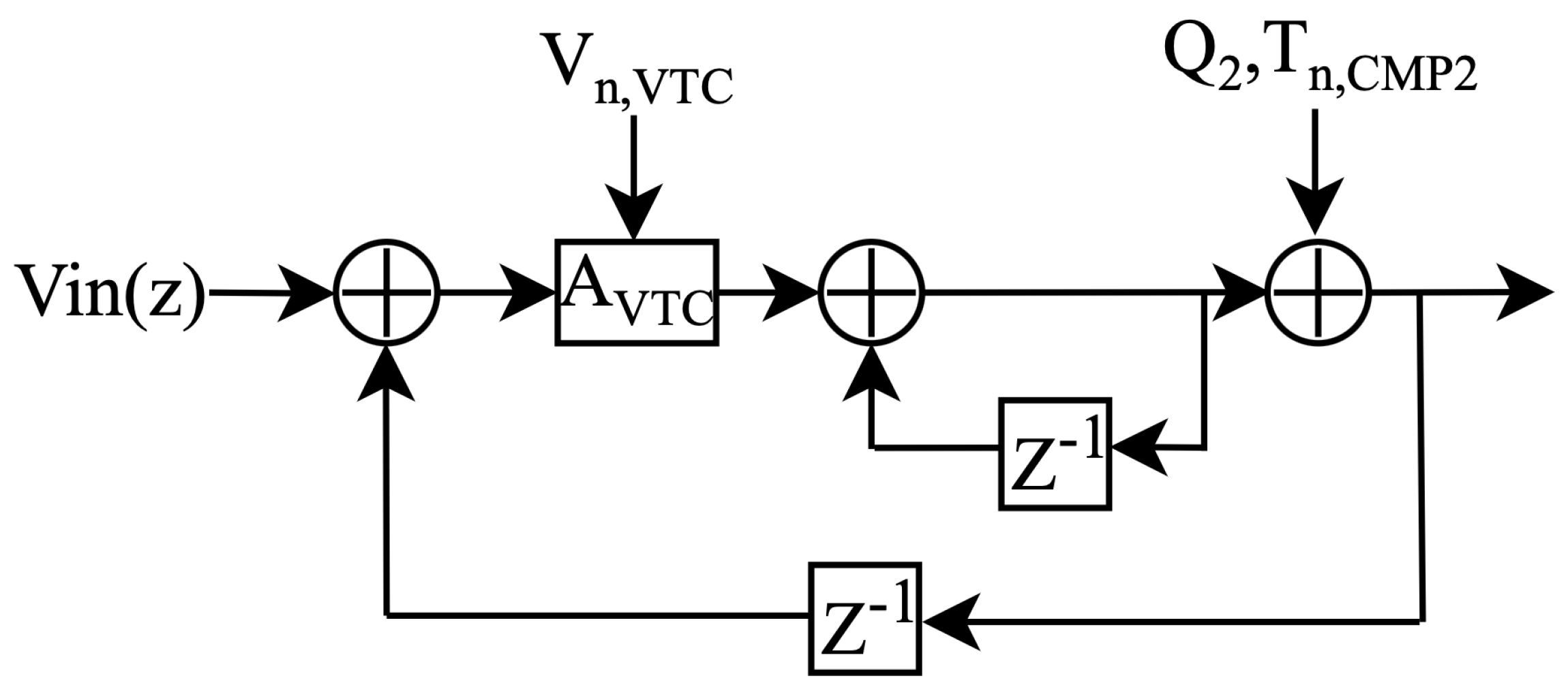
3. Non-Linearity Analysis of the ISDM Stage
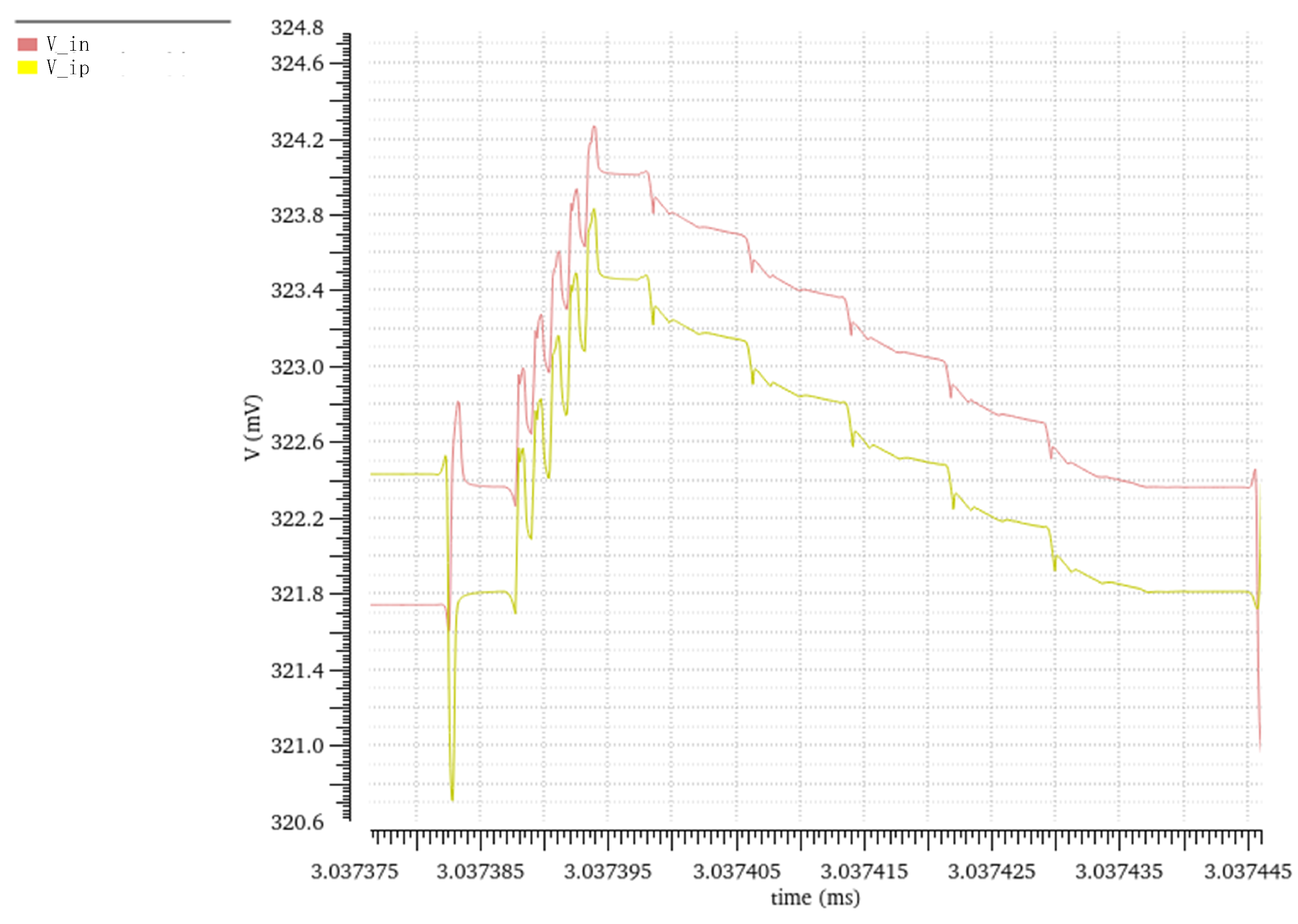
3.1. VCM Shift Induced by Kickback Noise
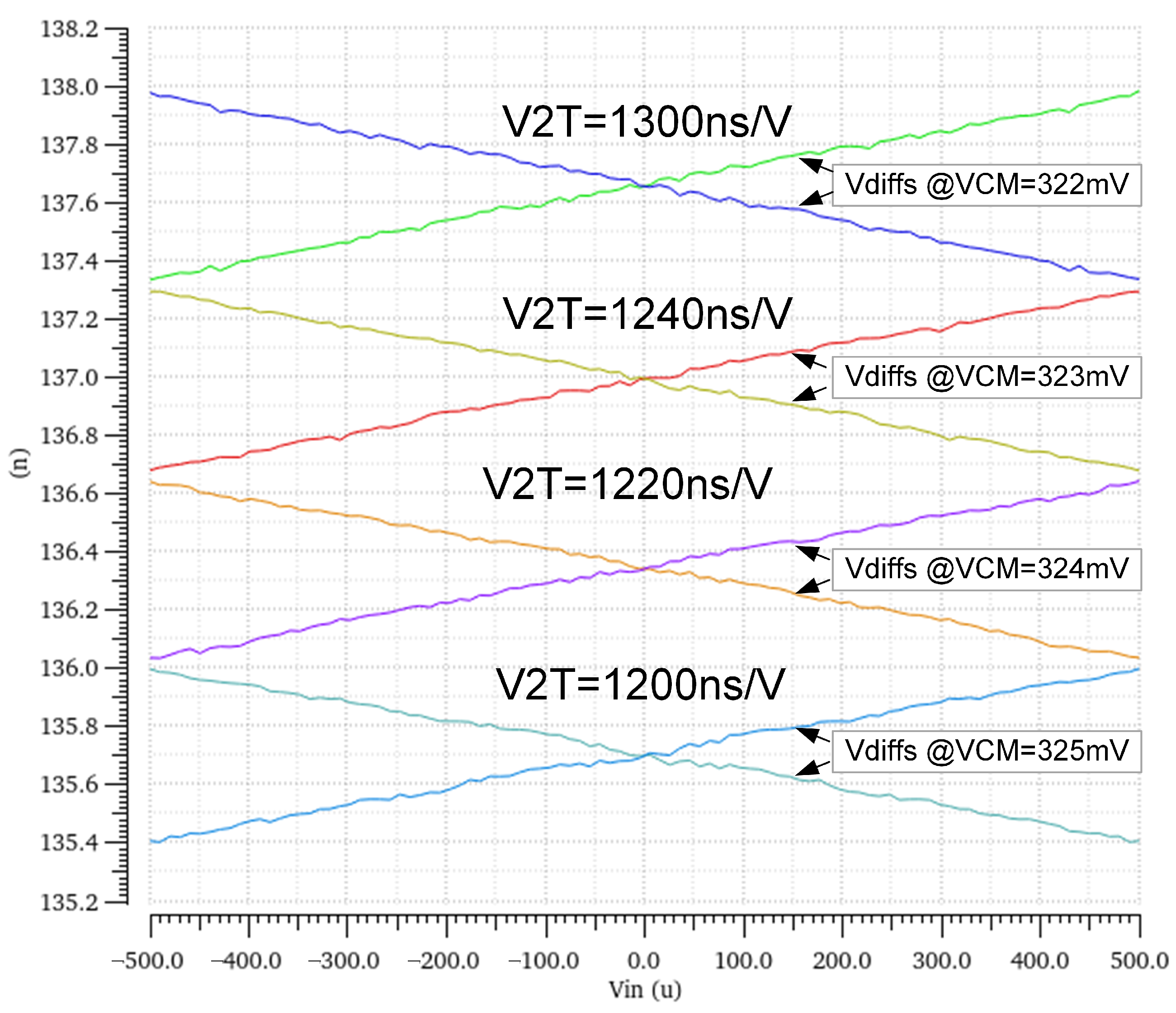
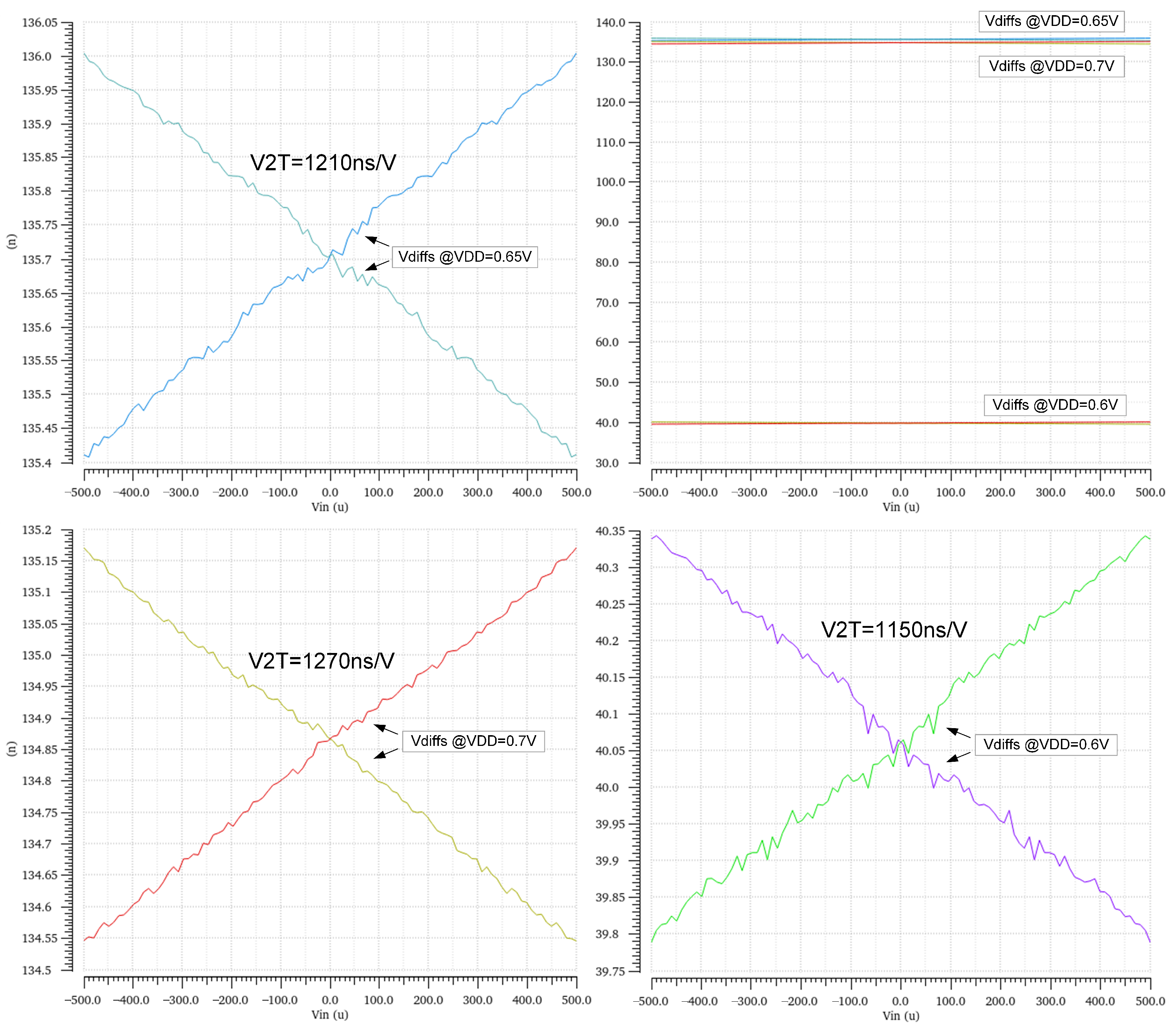
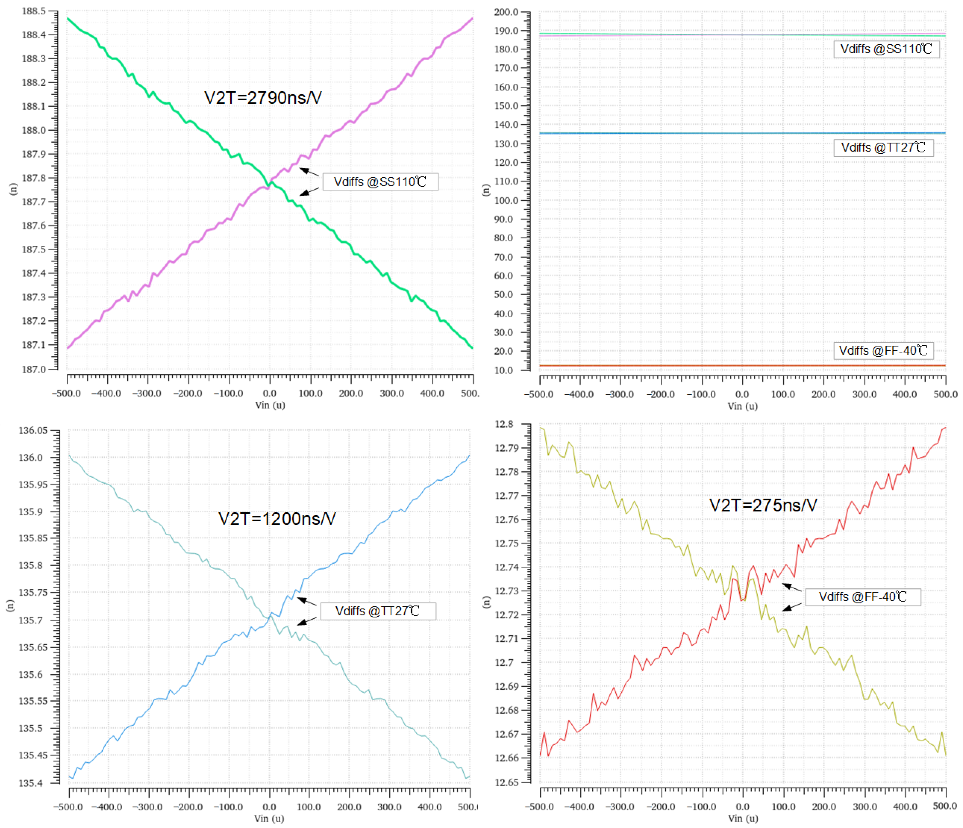
3.2. The VCM- and PVT-Sensitive V2T Term
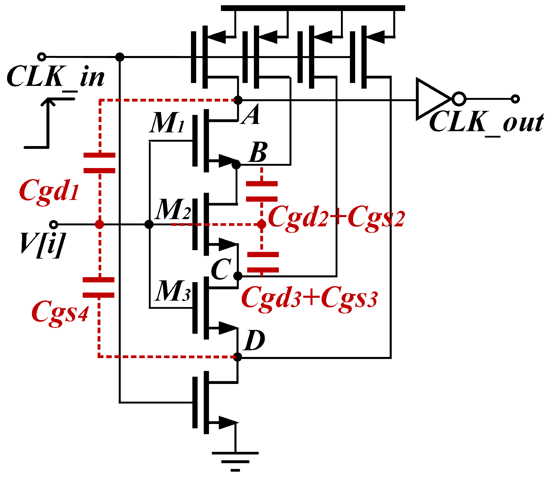
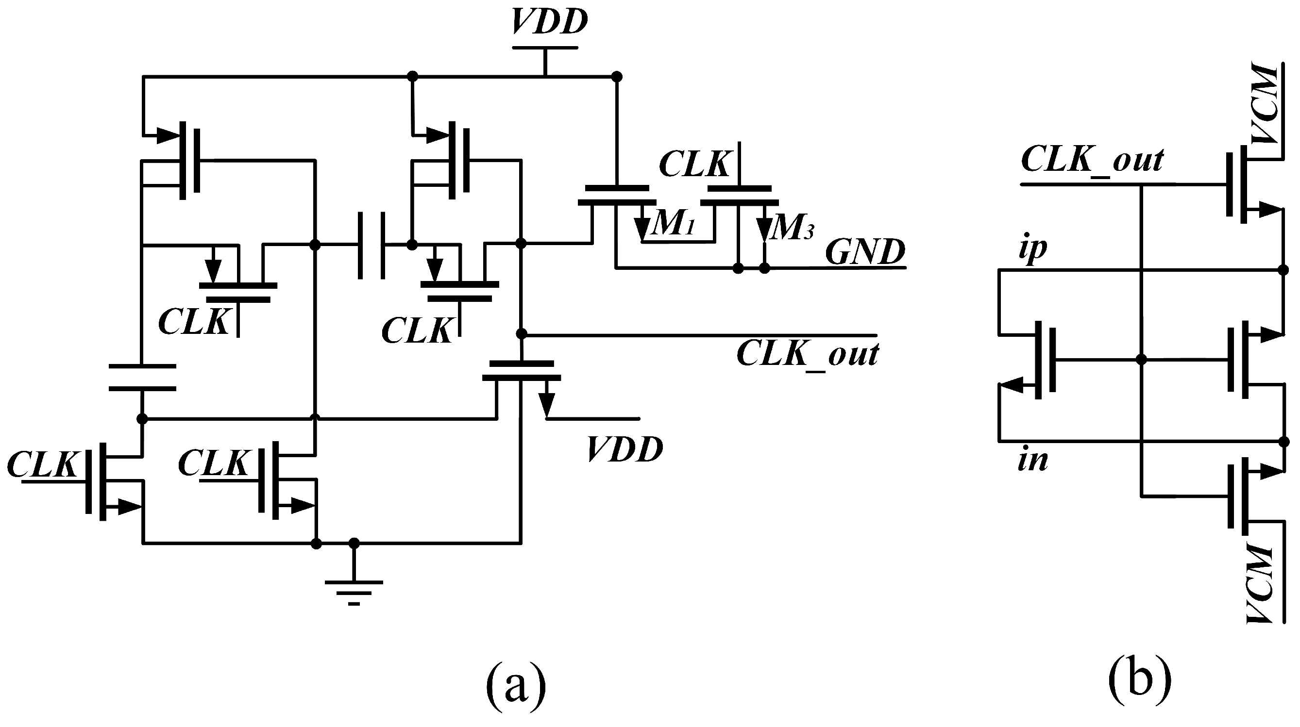
4. Circuit Implementation
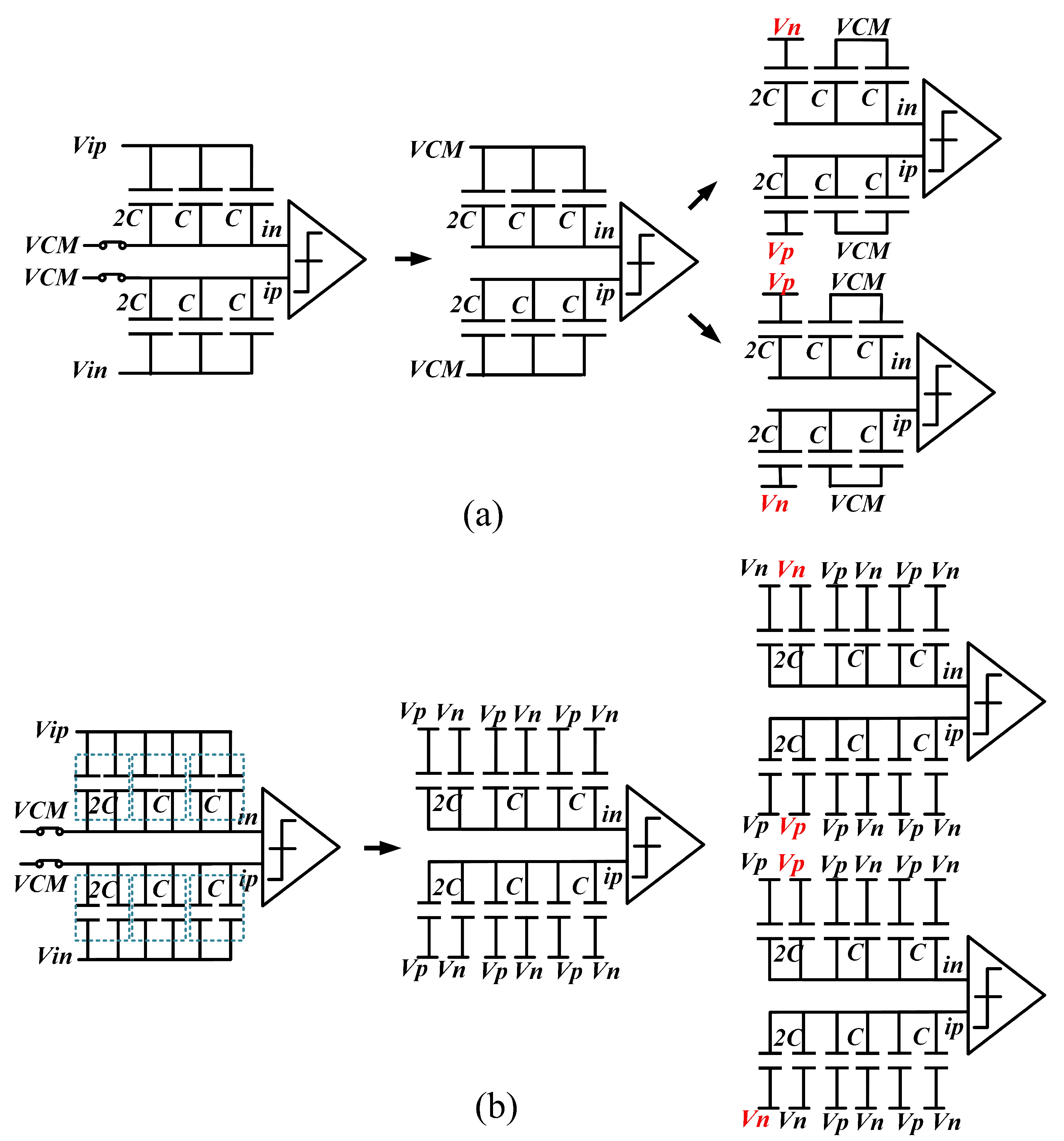
4.1. Modified MCS for CDAC
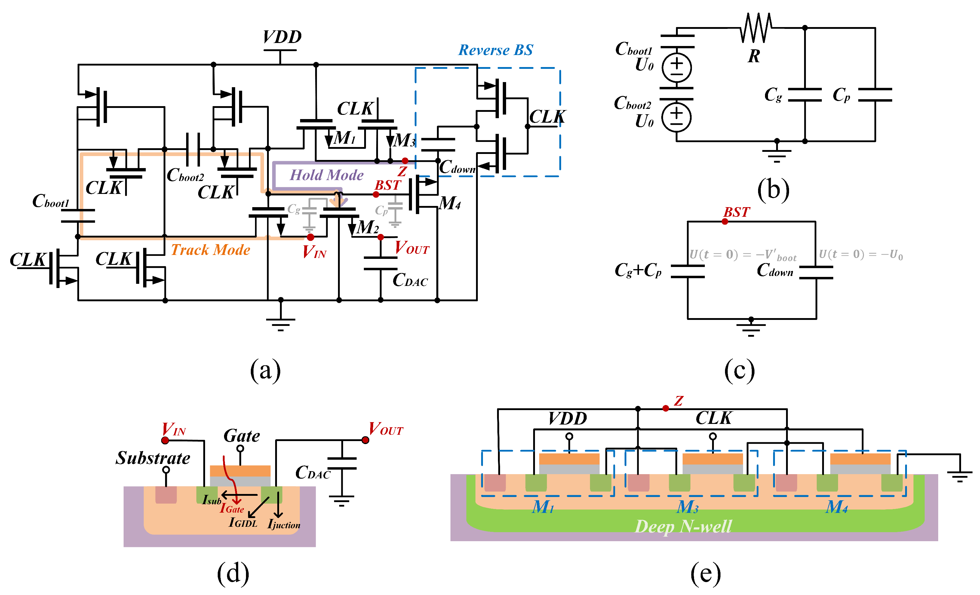
4.2. Bootstrapped Switch
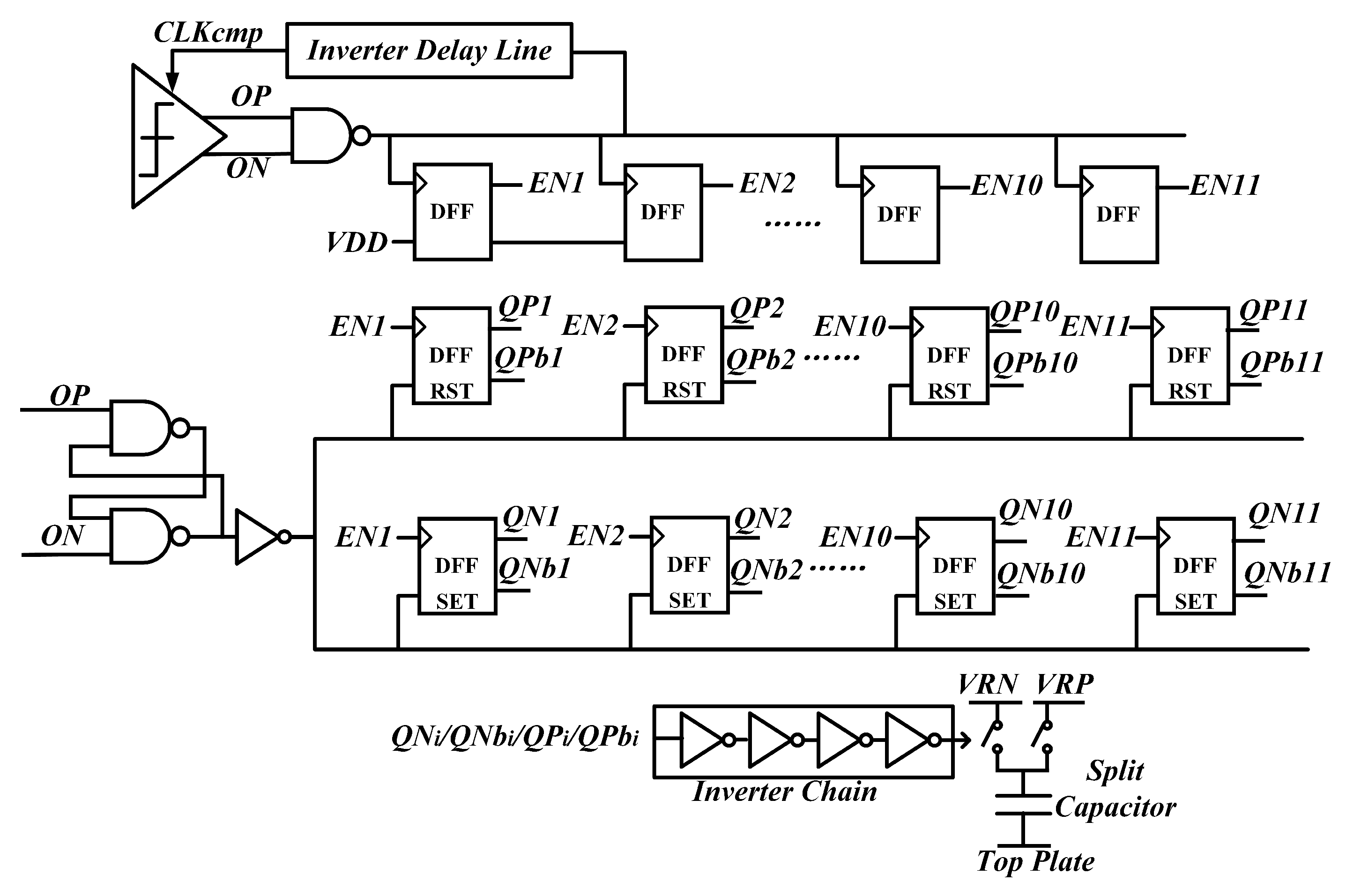
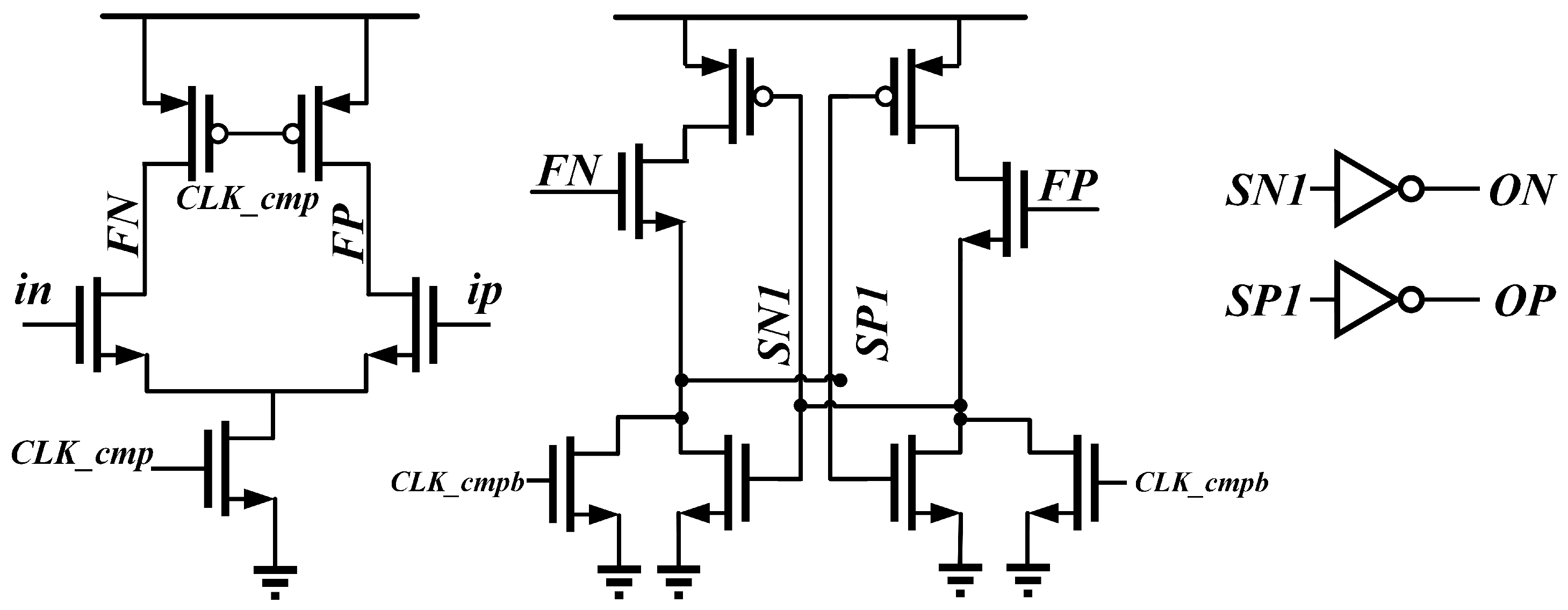
4.3. Comparator
4.4. CDAC
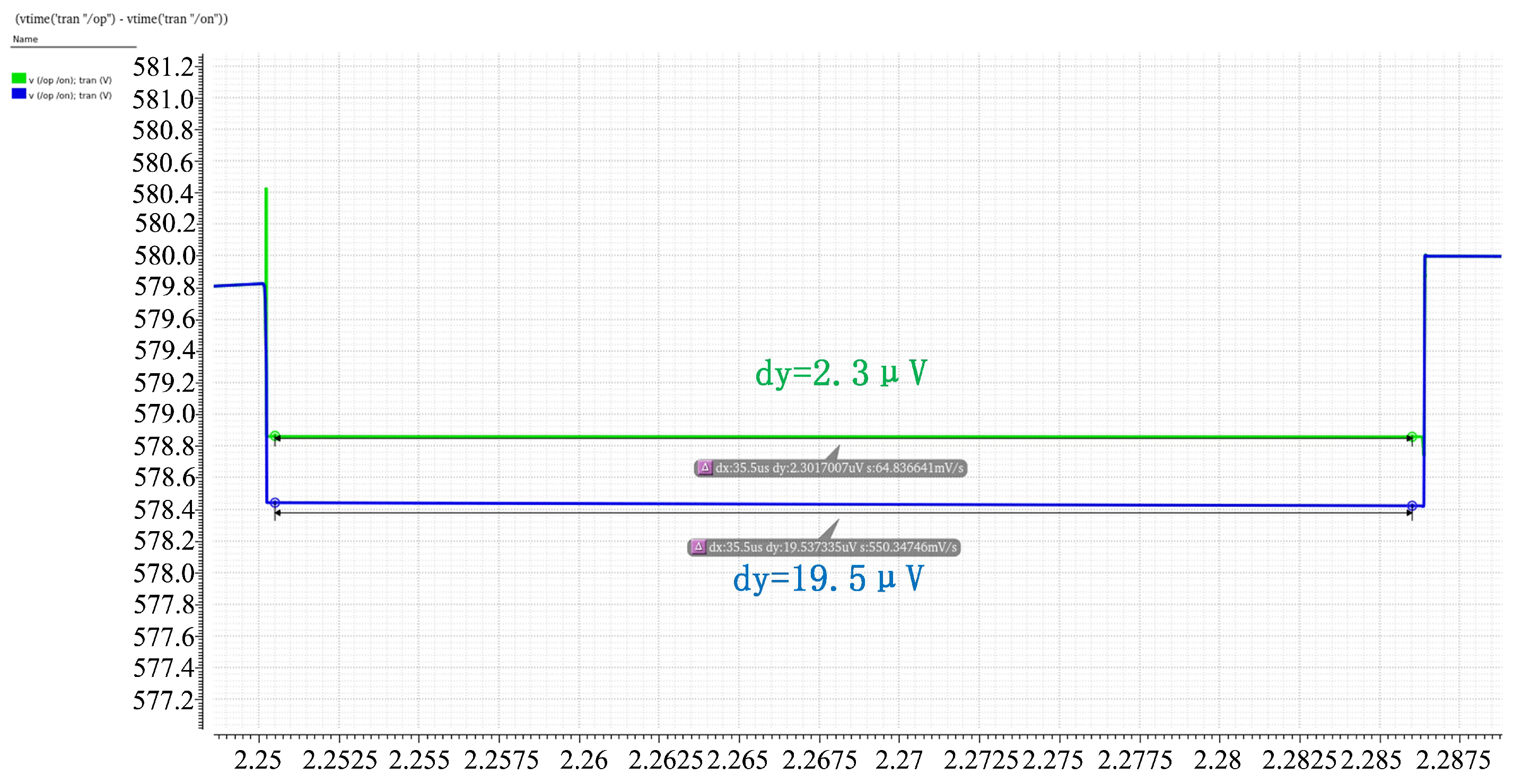
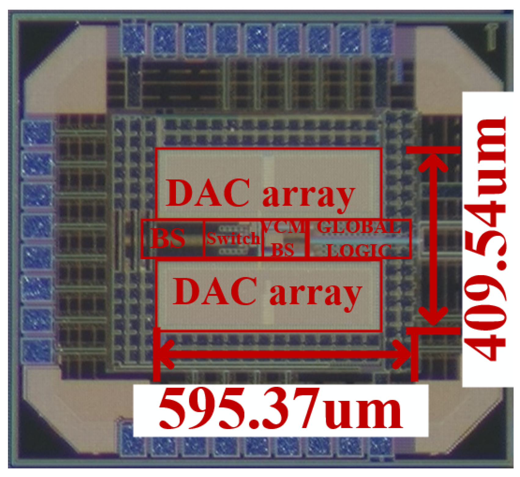
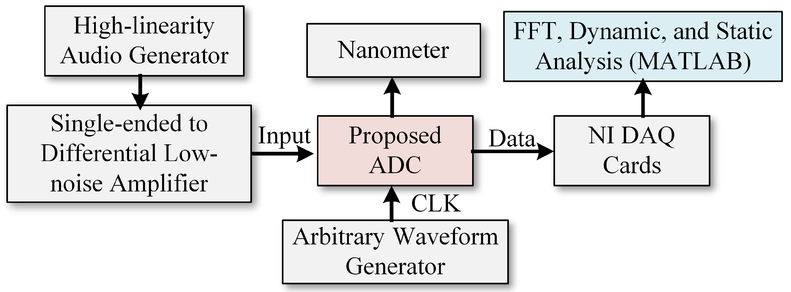
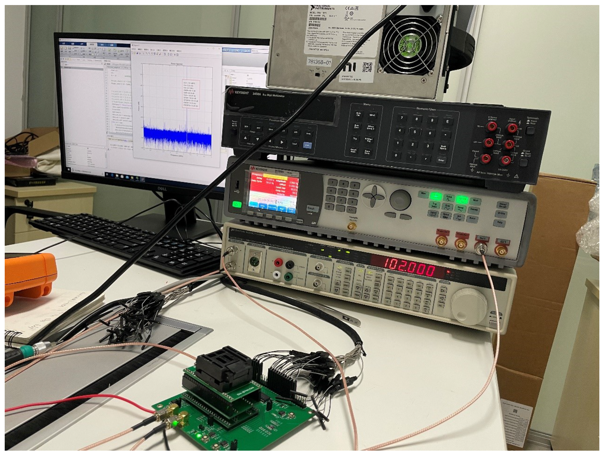
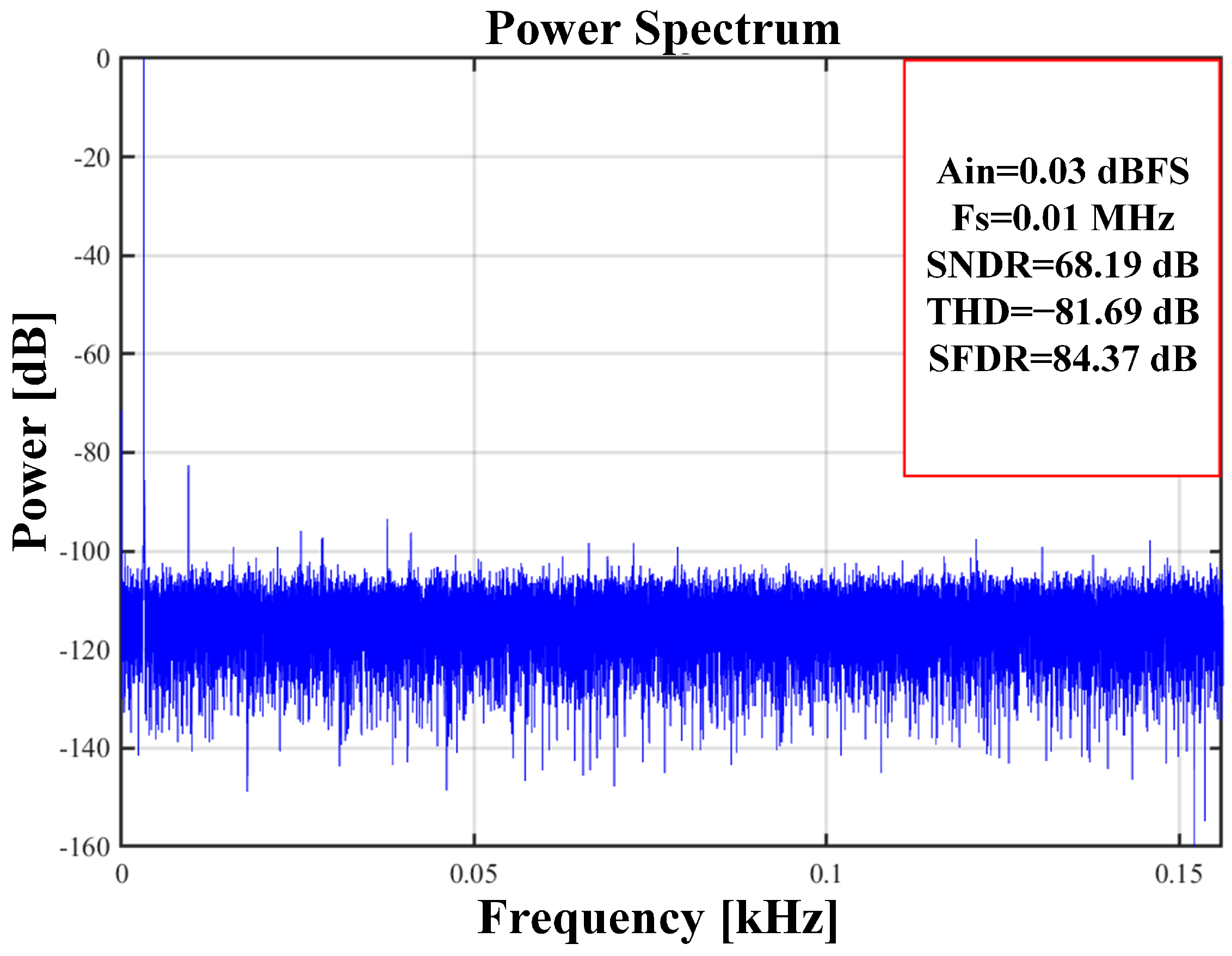
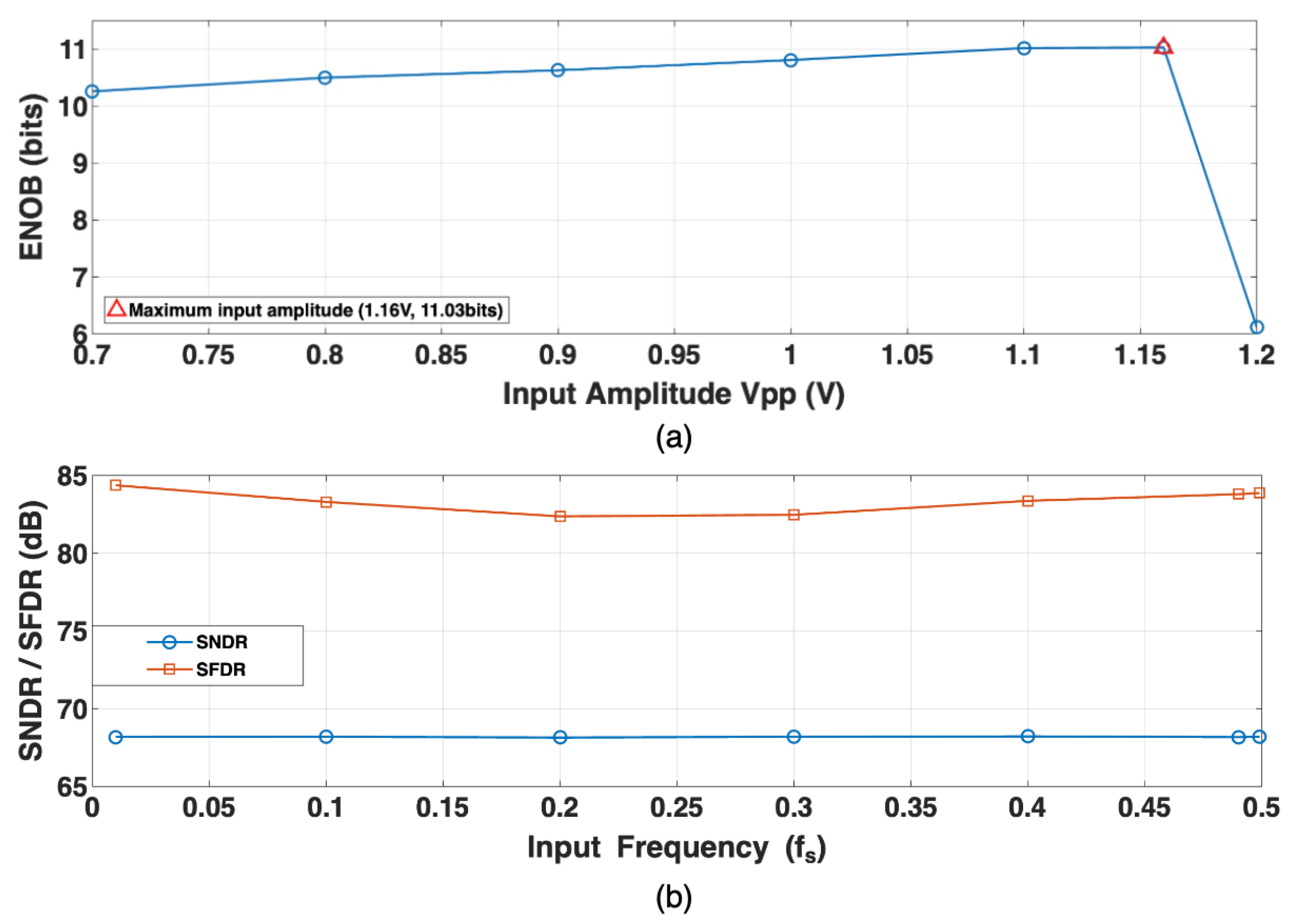
5. Measurement Results
6. Conclusions
Author Contributions
Funding
Data Availability Statement
Conflicts of Interest
References
- Shiue, M.-T.; Lo, Y.-F.; Jung, C.-Y. Design of an internal asynchronous 11-bit SAR ADC for biomedical wearable application. Electronics 2024, 13, 3549. [Google Scholar] [CrossRef]
- Lakshmi, P.V.; Musala, S.; Srinivasulu, A.; Ravariu, C. Design of a 0.4 V, 8.43 ENOB, 5.29 nW, 2 kS/s SAR ADC for implantable devices. Electronics 2023, 12, 4691. [Google Scholar] [CrossRef]
- Tang, X.; Liu, J.; Shen, Y.; Li, S.; Shen, L.; Sanyal, A.; Ragab, K.; Sun, N. Low-power SAR ADC design: Overview and survey of state-of-the-art techniques. IEEE Trans. Circuits Syst. I Regul. Pap. 2022, 69, 2249–2262. [Google Scholar] [CrossRef]
- Seo, M.-W.; Chu, M.; Jung, H.-Y.; Kim, S.; Song, J.; Bae, D.; Lee, S.; Lee, J.; Kim, S.-Y.; Lee, J. 2.45 e-RMS low random noise, 598.5 mW low-power, and 1.2 kfps high-speed 2-Mp global shutter CMOS image sensor with pixel-level ADC and memory. IEEE J. Solid-State Circuits 2022, 57, 1125–1137. [Google Scholar] [CrossRef]
- Jin, H.; Hu, W.; Zhao, Y.; Jiang, Y.; Ye, Y.; Wang, S.; Qin, Y. A 1.5 mm2 4-channel EEG/BIOZ acquisition ASIC with 15.2-bit 3-step ADC based on a signal-dependent low-power strategy. IEEE Trans. Biomed. Circuits Syst. 2023, 17, 1111–1124. [Google Scholar] [CrossRef]
- Yu, S.; Shi, X.; Zhou, Y.; Ma, D.; Zhang, Y.; Lu, W.; Chen, Z. A low-power DROIC with extended-counting ADC for uncooled infrared silicon diode detectors. IEEE Trans. Circuits Syst. II Express Briefs 2023, 70, 1881–1885. [Google Scholar] [CrossRef]
- Yazdani, B.; Jafarabadi Ashtiani, S. A low power fully differential level-crossing ADC with low power charge redistribution input for biomedical applications. IEEE Trans. Circuits Syst. II Express Briefs 2022, 69, 864–868. [Google Scholar] [CrossRef]
- Liu, L.; Qin, Z.; Yin, J.; Liao, X.; Tian, Y. A 16.8-ENOB, 3.5-μW fourth-order discrete-time delta-sigma ADC for biosignal acquisition applications. IEEE Trans. Circuits Syst. II Express Briefs 2024, 71, 1749–1753. [Google Scholar] [CrossRef]
- Hopf, Y.M.; Ossenkoppele, B.W.; Soozande, M.; Noothout, E.; Chang, Z.-Y.; Chen, C.; Vos, H.J.; Bosch, J.G.; Verweij, M.D.; de Jong, N.; et al. A pitch-matched transceiver ASIC with shared hybrid beamforming ADC for high-frame-rate 3-D intracardiac echocardiography. IEEE J. Solid-State Circuits 2022, 57, 3228–3242. [Google Scholar] [CrossRef]
- Guo, P.; Fool, F.; Chang, Z.-Y.; Noothout, E.; Vos, H.J.; Bosch, J.G.; de Jong, N.; Verweij, M.D.; Pertijs, M.A.P. A 125 μm pitch-matched transceiver ASIC with micro-beamforming ADC and multi-level signaling for 3-D transfontanelle ultrasonography. IEEE J. Solid-State Circuits 2024, 59, 2604–2617. [Google Scholar] [CrossRef]
- ElAnsary, M.; Xu, J.; Filho, J.S.; Dutta, G.; Long, L.; Tejeiro, C.; Shoukry, A.; Tang, C.; Kilinc, E.; Joshi, J.; et al. Bidirectional peripheral nerve interface with 64 second-order opamp-less ΔΣ ADCs and fully integrated wireless power/data transmission. IEEE J. Solid-State Circuits 2021, 56, 3247–3262. [Google Scholar] [CrossRef]
- Zhang, Y.; Yang, C.; Sun, J.; Li, Z.; Gao, H.; Luo, Y.; Xu, K.; Pan, G.; Zhao, B. A wireless headstage system based on neuralrecording chip featuring 315 nW kickback-reduction SAR ADC. IEEE Trans. Biomed. Circuits Syst. 2023, 17, 105–115. [Google Scholar] [CrossRef] [PubMed]
- Wang, S.-H.; Hung, C.-C. A 0.3V 10b 3MS/s SAR ADC with comparator calibration and kickback noise reduction for biomedical applications. IEEE Trans. Biomed. Circuits Syst. 2020, 14, 558–569. [Google Scholar] [CrossRef] [PubMed]
- Li, M.; Huo, Y.; Song, S.; Qu, W.; Ye, L.; Zhao, M.; Tan, Z. A 62.2dB SNDR event-driven level-crossing ADC with SAR-assisted delay compensation loop for time-sparse biomedical signal acquisition. IEEE Trans. Biomed. Circuits Syst. 2024, 19, 344–356. [Google Scholar] [CrossRef]
- Lee, S.; Kang, H.; Lee, M. A 2.72fJ/conv 13b 2MS/s SAR ADC using dynamic capacitive comparator with wide input common mode. In Proceedings of the IEEE International Solid-State Circuits Conference (ISSCC), San Francisco, CA, USA, 18–22 February 2024; pp. 184–186. [Google Scholar]
- He, X.; Gu, M.; Jiang, H.; Zhong, Y.; Sun, N.; Jie, L. A 71dB SNDR 200MHz BW interleaved pipe-SAR ADC with a shared residue integrating amplifier achieving 173dB FoMs. In Proceedings of the IEEE International Solid-State Circuits Conference (ISSCC), San Francisco, CA, USA, 18–22 February 2024; pp. 172–174. [Google Scholar] [CrossRef]
- Cheng, K.-C.; Chang, S.-J.; Chen, C.-C.; Hung, S.-H. A 94.3dB SNDR 184dB FoMs 4th-order noise-shaping SAR ADC with dynamic-amplifier-assisted cascaded integrator. In Proceedings of the IEEE International Solid-State Circuits Conference (ISSCC), San Francisco, CA, USA, 18–22 February 2024; pp. 180–182. [Google Scholar] [CrossRef]
- Chung, J.-H.; Kim, Y.-D.; Park, C.-U.; Park, K.-W.; Oh, D.-R.; Seo, M.-J.; Ryu, S.-T. A 1.5-MHz BW 81.2-dB SNDR dual-residue pipeline ADC with a fully dynamic noise-shaping interpolating SAR ADC. IEEE J. Solid-State Circuits 2024, 59, 2481–2491. [Google Scholar] [CrossRef]
- Wei, C.; Wei, R.; Huang, L.; Huang, G.; Lai, J.; Tan, Z. An energy-efficient discrete-time delta–sigma modulator with dynamic-range enhancement and tri-level CDAC. IEEE J. Solid-State Circuits 2024, 59, 2848–2857. [Google Scholar] [CrossRef]
- Meng, L.; Chen, J.; Zhao, M.; Tan, Z. A partially feedback NSSAR embedded third-order delta–sigma modulator with gain-boosted two-stage FIAs. IEEE J. Solid-State Circuits 2024, 59, 2735–2746. [Google Scholar] [CrossRef]
- Lee, D.-H.; Lozada, K.E.; Kim, Y.-D.; Kim, H.-J.; Cho, Y.; Choi, M.; Ryu, S.-T. A 25-kHz-BW 97.4-dB-SNDR SAR-assisted continuous-time 1-0 MASH delta–sigma modulator with digital noise coupling. IEEE J. Solid-State Circuits 2024, 59, 3232–3241. [Google Scholar] [CrossRef]
- An, K.-C.; Narasimman, N.; Kim, T.T.-H. A 0.6-to-1.2 V scaling-friendly discrete-time OTA-free linear VCO-based ΔΣ ADC suitable for DVFS. IEEE Trans. Circuits Syst. I Regul. Pap. 2024, 71, 1481–1494. [Google Scholar] [CrossRef]
- Hsieh, S.-E.; Hsieh, C.-C. A 0.4-V 13-bit 270-kS/s SAR-ISDM ADC with opamp-less time-domain integrator. IEEE J. Solid-State Circuits 2019, 54, 1648–1656. [Google Scholar] [CrossRef]
- Chan, Y.-C.; Chang, C.-W.; Lee, T.-C. A 0.9-V 50-MS/s 67.3-dB-SNDR SAR-ISDM ADC with an oscillator-based integrator. IEEE Trans. Circuits Syst. II Express Briefs 2023, 70, 3263–3267. [Google Scholar] [CrossRef]
- Zhu, Y.; Liu, T.; Kaile, S.K.; Kiran, S.; Yi, I.-M.; Liu, R.; Diaz, J.C.G.; Hoyos, S.; Palermo, S. A 38-GS/s 7-bit pipelined-SAR ADC with speed- enhanced bootstrapped switch and output level shifting technique in 22-nm FinFET. IEEE J. Solid-State Circuits 2023, 58, 2300–2313. [Google Scholar] [CrossRef]
- Swindlehurst, E.; Jensen, H.; Petrie, A.; Song, Y.; Kuan, Y.-C.; Chang, M.-C.F.; Wu, J.-T.; Chiang, S.-H.W. An 8-bit 10-GHz 21-mW time-interleaved SAR ADC with grouped DAC capacitors and dual-path bootstrapped switch. IEEE J. Solid-State Circuits 2021, 56, 83–86. [Google Scholar] [CrossRef]
- Kim, T.; Chae, Y. A 2.1 mW 2 MHz-BW 73.8 dB-SNDR buffer-embedded noise-shaping SAR ADC. IEEE Trans. Circuits Syst. I Regul. Pap. 2021, 68, 5029–5037. [Google Scholar] [CrossRef]
- Huang, M.; Lu, Y.; Hu, T.; Martins, R.P. A hybrid boost converter with cross-connected flying capacitors. IEEE J. Solid-State Circuits 2021, 56, 2102–2112. [Google Scholar] [CrossRef]
- Zhuang, H.; Cao, Q.; Peng, X.; Tang, H. A bootstrapped switch with accelerated rising speed and reduced on-resistance. In Proceedings of the IEEE International Symposium for Circuits and Systems (ISCAS), Daegu, Republic of Korea, 22–28 May 2021; pp. 1–5. [Google Scholar] [CrossRef]
- Lin, J.-Y.; Hsieh, C.-C. A 0.3 V 10-bit SAR ADC with first 2-bit guess in 90-nm CMOS. IEEE Trans. Circuits Syst. I Regul. Pap. 2017, 64, 562–572. [Google Scholar] [CrossRef]
- Hsieh, S.-E.; Hsieh, C.-C. A 0.44-fJ/conversion-step 11-bit 600-kS/s SAR ADC with semi-resting DAC. IEEE J. Solid-State Circuits 2018, 53, 2595–2603. [Google Scholar] [CrossRef]
- Hariprasath, V.; Guerber, J.; Lee, S.-H.; Moon, U.-K. Merged capacitor switching based SAR ADC with highest switching energy efficiency. Electron. Lett 2010, 46, 620–621. [Google Scholar] [CrossRef]
- Lin, Y.-Z.; Tsai, C.-H.; Tsou, S.-C.; Chu, R.-X.; Lu, C.-H. A 2.4-mW 25-mHz BW 300-MS/s passive noise shaping SAR ADC with noise quantizer technique in 14-nm CMOS. In Proceedings of the IEEE Symposium on VLSI Circuits, Kyoto, Japan, 5–8 June 2017; pp. C234–C235. [Google Scholar] [CrossRef]
- Sadollahi, M.; Hamashita, K.; Sobue, K.; Temes, G.C. An 11-bit 250-nW 10-kS/s SAR ADC with doubled input range for biomedical applications. IEEE Trans. Circuits Syst. I Regul. Pap. 2018, 61, 61–73. [Google Scholar] [CrossRef]


| TT (27 °C) | SS (−40 °C) | FF (85 °C) | |
|---|---|---|---|
| ENOB [bit] | 12.03 | 11.79 | 12.3 |
| SNDR [dB] | 74.1 | 72.7 | 75.8 |
| SFDR [dB] | 86.3 | 82.2 | 88.5 |
| Power [µW] | 0.38 | 0.36 | 0.41 |
| TCAS2 [24] | VLSI [33] | TCAS1 [34] | JSSC [23] | This Work | |
|---|---|---|---|---|---|
| Process [nm] | 40 | 14 | 180 | 90 | 180 |
| ADC type | SAR–ISDM | NS-SAR | SAR | SAR | SAR–ISDM |
| Supply [V] | 0.9 | 1.0 | 0.75 | 1.2 | 0.6 (min. 0.575 V) |
| [S/s] | 50 M | 400 M | 10 k | 50 M | 10 k |
| Resolution [bit] | 13 | 10 | 11 | 13 | 13 |
| SFDR [dB] | 72.2 | 81.2 | 72.0 | 85 | 84.4 |
| SNDR [dB] | 67.3 | 66.2 | 60.5 | 71 | 68.2 |
| Power [µW] | 2590 | 2800 | 0.25 | 4200 | 0.42 |
| FOMw [fJ/conv.-s] | 16.76 | 25.3 | 28.8 | 29.0 | 20.05 |
Disclaimer/Publisher’s Note: The statements, opinions and data contained in all publications are solely those of the individual author(s) and contributor(s) and not of MDPI and/or the editor(s). MDPI and/or the editor(s) disclaim responsibility for any injury to people or property resulting from any ideas, methods, instructions or products referred to in the content. |
© 2025 by the authors. Licensee MDPI, Basel, Switzerland. This article is an open access article distributed under the terms and conditions of the Creative Commons Attribution (CC BY) license (https://creativecommons.org/licenses/by/4.0/).
Share and Cite
Li, X.; Yoshioka, K.; Wang, Z.; Lin, J.; Zhu, C. A 0.6 V 68.2 dB 0.42 µW SAR-ΣΔ ADC for ASIC Chip in 0.18 µm CMOS. Electronics 2025, 14, 2030. https://doi.org/10.3390/electronics14102030
Li X, Yoshioka K, Wang Z, Lin J, Zhu C. A 0.6 V 68.2 dB 0.42 µW SAR-ΣΔ ADC for ASIC Chip in 0.18 µm CMOS. Electronics. 2025; 14(10):2030. https://doi.org/10.3390/electronics14102030
Chicago/Turabian StyleLi, Xinyu, Kentaro Yoshioka, Zhongfeng Wang, Jun Lin, and Congyi Zhu. 2025. "A 0.6 V 68.2 dB 0.42 µW SAR-ΣΔ ADC for ASIC Chip in 0.18 µm CMOS" Electronics 14, no. 10: 2030. https://doi.org/10.3390/electronics14102030
APA StyleLi, X., Yoshioka, K., Wang, Z., Lin, J., & Zhu, C. (2025). A 0.6 V 68.2 dB 0.42 µW SAR-ΣΔ ADC for ASIC Chip in 0.18 µm CMOS. Electronics, 14(10), 2030. https://doi.org/10.3390/electronics14102030