1. Introduction
As a critical component of computer systems, the performance and integration of memory play a significant role in improving the efficiency of the whole system. Memory technologies encompass random access memory (static random access memory and dynamic random access memory), read-only memory (programmable read-only memory, erasable programmable read-only memory, and electrically erasable programmable read-only memory), and novel memory (phase change memory, magnetoresistive random access memory, resistive random access memory, and ferroelectric random access memory). SRAM occupies an important position due to the superiority of its high access speed, high reliability, and process compatibility. However, conventional SRAM is facing challenges such as high power consumption and integration limitations, making future improvements necessary. Consequently, research on novel SRAM with high performance and low power consumption has become a strategic direction.
From the perspective of circuit design, the performance improvement of SRAM can be achieved by optimizing the structure of the memory cell and peripheral circuit. Ref. [
1] proposed a novel seven-transistor SRAM cell using multi-threshold voltage (multi-Vth) transistors to enable low supply voltage and high-speed operation. However, this structure may have the problem of stored data being destroyed and the write operation not being able to be performed normally at low power supply voltage, which will limit its utilization in ultra-low power applications. Ref. [
2] proposed an adiabatic 9T SRAM cell, which includes a transmission gate controlled by a write word line (WWL) signal to enable the memory cell to operate as an adiabatic structure during data writing. With an NMOS transistor as a switch device, the adiabatic structure can minimize short-circuit current in write mode and then achieve a reduction in power consumption. The circuit proposed in [
2] demonstrates a significant improvement in energy consumption compared to conventional adiabatic circuits. However, the static noise margin of the adiabatic 9T cell is 54% lower than the conventional cell, which means that the adiabatic 9T cell is more susceptible to noise during read, write, and standby modes. Ref. [
3] compared the performance of adiabatic logic and non-adiabatic logic SRAM in both the CMOS and FinFET processes. The study demonstrated that the FinFET-based adiabatic logic SRAM cell achieved a 99% reduction in power consumption compared to conventional SRAM with the same process nodes. Ref. [
4] proposed a 12T SRAM cell with low power consumption and high stability. Simulations were conducted to verify the performance of the 12T cell using the CMOS 40 nm, CMOS 90 nm, and 14 nm FinFET processes. The results showed that the SRAM cell based on the 14 nm FinFET process had a higher static noise margin, with only 95.1 pW power consumption. However, it had a larger area due to six additional transistors compared to a conventional 6T cell, which may affect its integrated density and is not suitable for high-density memory.
From the perspective of process, the conventional silicon-based process is approaching its physical limits, mainly manifest as the quantum tunneling effect and short channel effect. The scaling down of transistor size and channel length induces a remarkable degradation in gate control over the channel, accompanied by increased leakage current and consequently a substantial rise in static power consumption; this may have an inevitable negative impact on the overall energy efficiency. In order to transcend the physical limits of silicon-based devices, exploring novel materials has become the focus in the post-Moore era. In recent years, CNTs have been widely used in the design of various novel memories as a potential material. Ref. [
5] proposed a novel carbon nanotube field-effect transistor (CNTFET) 8T SRAM cell, which separates read operation from write operation. During the write operation, the circuit does not include a race between the latch and the access transistors. The write operation only uses two pull-up PMOS transistors. This structure can effectively improve write speed and reduce power consumption. Transistor stacking is used for read operations to enable better low-voltage operation. CNTFET has low power characteristics. The novel 8T cell proposed in Ref. [
5] could achieve significant leakage power reduction. The results showed that the static power consumption of the CNTFET 8T SRAM cell was 97.94% lower than the conventional CNTFET 6T SRAM cell, and the write power consumption was also lower. Simulations of conventional CNTFET 6T SRAM cells were conducted in [
6] through Verilog-A behavioral modeling. After a series of performance comparisons with 6T cells in conventional CMOS processes, the potential of CNTFET in memory design was reaffirmed. Ref. [
7] evaluated the performance of 6T, 7T, 8T, and 10T SRAM cells implemented with both CNTFET and CMOS processes, revealing that carbon-based designs achieved superior power efficiency with a 98% reduction in total power consumption compared to silicon-based designs. The influence of different chiralities on CNTFET performance has also been previously discussed, and the chirality has been optimized to reduce power consumption. The design of a large-scale CNTFET SRAM array and 10T SRAM cell was first experimentally implemented in [
8]. Results showed the 10T SRAM cell could operate at voltages as low as 300 mV. A full-contact structure was introduced in [
9], which reduced the contacted gate pitch (CGP) to 55 nm, corresponding to the 10 nm silicon-based node. The CNTFET maintained performance superiority over silicon-based transistors. Ref. [
9] compared the performance of optimized carbon-based SRAM with silicon-based 90 nm SRAM. The results showed that compared with the silicon-based 90 nm SRAM, the carbon-based SRAM significantly reduced static power consumption and dynamic power consumption by 80.18% and 21.80%, respectively. In addition to CNTFETs, ferroelectric field-effect transistors (FeFETs) have also been widely employed in memory cell design and in-memory computing due to their non-volatility and low power consumption. FeFETs are transistors formed by integrating ferroelectric materials—materials exhibiting spontaneous polarization—into MOS structures, thereby enabling both storage and computation capabilities. Ref. [
10] proposed a low-power edge detection hardware system with HfO2-based FeFET. The proposed hardware system was able to achieve efficient image edge detection at low power consumption (~10 fJ/per operation), which is one of the most potential non-volatile memories for energy-efficient computing. Ref. [
11] compared the performance of SRAMs based on FinFET and FeFET processes. It demonstrated that FeFET-based FinFET (FEFINFET) SRAM exhibited higher read stability and less access time. However, the write delay increased due to the higher equivalent gate capacitance of the FEFINFET. In-memory computing designs based on FeTFETs have achieved energy efficiencies of 48.03 TOPS/W [
12] and 2866 TOPS/W [
13] at the system level.
CNTFETs exhibit high carrier mobility, low power consumption, and compatibility with low-temperature processes, meaning carbon-based SRAMs show great potential for high-performance and low-power applications. However, CNTFETs still face considerable challenges in large-scale fabrication, contact performance, and cost. FeFETs offer non-volatility and can function at extremely low voltages. Their polarization properties enable FeFETs to serve as both non-volatile memory cells (NV SRAM/eNVM) and computing units for analog matrix multiplication in in-memory computing. However, the ferroelectricity of FeFETs only exists below a certain temperature. Slight temperature deviation can cause the material to degrade into paraelectric or antiferroelectric phases. Moreover, FeFETs rely on ferroelectric polarization switching, which limits their speed and leads to degradation of the switching window over repeated use. In contrast, the metal–oxide–semiconductor field-effect transistor (MOSFET), owing to its mature manufacturing process and economical efficiency, maintains a dominant position in the electronics industry, although it exhibits inherent limitations in mobility and power consumption. To address these challenges, a novel carbon–silicon heterogeneous-integrated SRAM technology is proposed in this paper. The carbon–silicon heterogeneous-integrated SRAM technology combines the high mobility, low power consumption, and ballistic transport capability of CNTs with mature silicon-based fabrication processes, which enables significant optimization of access time and power consumption of the overall circuit. In addition, a novel read/write-decoupled SRAM cell is proposed to further improve the low-power performance of SRAMs. The read/write-decoupled SRAM cell is composed of nine transistors. When SRAM is in standby mode, utilization of this cell can effectively reduce leakage current, thereby reducing the static power consumption of the overall circuit.
2. Circuit Design
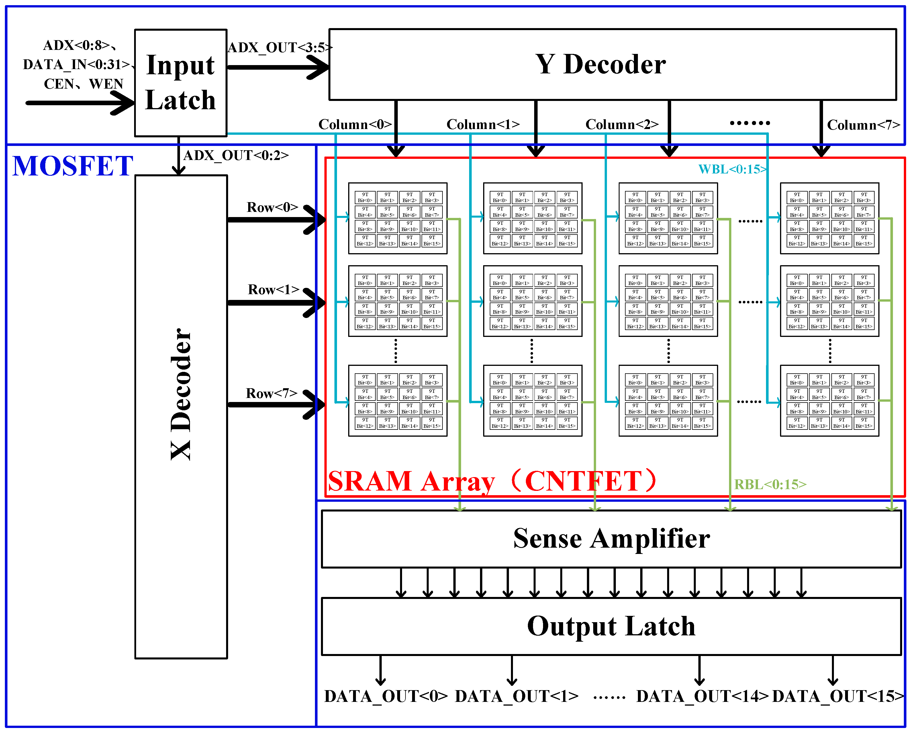
This work implemented a 64 × 16-bit carbon–silicon heterogeneous-integrated SRAM circuit with the proposed novel 9T cell using a silicon-based 55 nm process and a carbon-based 500 nm process. The block diagram of the proposed SRAM is shown in
Figure 1. The SRAM circuit consists of five primary functional blocks: input latch, address decoder, SRAM memory array, sense amplifier, and output latch. Among these, the input latch, decoder, sense amplifier, and output latch(outlined in blue) were designed using a silicon-based 55 nm process, while the memory array(outlined in red) was implemented with a carbon-based 500 nm process. As conventional silicon-based processes approach their physical limits, the scaling down of channel length induces a remarkable degradation in gate control over the channel, accompanied by increased leakage current and consequently a substantial rise in static power consumption. The memory array occupies over half of the SRAM area. Employing a carbon-based process for its design can significantly reduce power consumption and enhance overall energy efficiency. Furthermore, CNTFET demonstrates compatibility with silicon-based processes, enabling heterogeneous integration design and improving integration density. The operational principle of the proposed SRAM is that input signals are initially latched by the input latch, and the latched address signals are subsequently processed by the decoder to access the corresponding memory array for read/write operations. During a read operation, the sense amplifier amplifies the subtle voltage differential generated by the memory cell to determine the stored data. Finally, the processed data from the sense amplifier are transferred to the output latch to ensure the stability and reliability of the output data.
The read/write operation timing of the proposed SRAM is shown in
Figure 2. SRAM enters standby mode when the enable signal (CEN) is high. When CEN is pulled down to low and the write enable signal (WEN) is high, the read operation is triggered at the rising edge of CLK, as shown in
Figure 2a, where t
ar is the access time of the read operation. Conversely, when both CEN and WEN are pulled down to low, the write operation is triggered at the rising edge of CLK, as shown in
Figure 2b, where t
aw is the access time of the write operation.
2.1. Carbon Nanotube Field-Effect Transistor (CNTFET)
The conventional silicon-based MOSFET is approaching physical limits, being confronted with the short-channel effect, soaring static power consumption, and quantum tunneling leakage currents at sub-5 nm technology nodes. CNTFET is considered to be one of the most promising technologies to improve the performance of integrated circuits in the post-Moore era due to its high mobility, one-dimensional ballistic transport capability, low power consumption, and other characteristics.
The CNTFET is composed of carbon nanotubes (single-walled or multi-walled), a gate, a source, and a drain. The carbon nanotube is used as the conducting channel, and the carrier transport characteristics are regulated by the gate electric field. Based on the position of the gate, carbon nanotubes can be classified into top-gate CNTFET (
Figure 3a) and gate-all-around CNTFET (
Figure 3b). The gate of the top-gate CNTFET is stacked above the carbon nanotube channel, with enhanced gate control ability. The top-gate CNTFET is applicable to high-performance logic circuits and carbon–silicon heterogeneous-integrated SRAM designs. The gate-all-around CNTFET completely wraps the CNT channel through the atomic layer deposition technology to form a fully enclosed electric field, which has the optimal electrostatic control ability and superior suppression of short-channel effects. However, the fabrication process exhibits extremely high complexity and requires nanoscale alignment accuracy. The gate-all-around CNTFET is applicable to ultra-low-power nanoelectronic devices and quantum computing units.
CNTs exhibit significant advantages in memory applications due to their high carrier mobility, low power consumption, and compatibility with low-temperature fabrication processes. The high carrier mobility of CNTs improves the read/write speed of memory devices, while their low power consumption characteristic contributes to reducing overall system energy consumption. Furthermore, the low-temperature process compatibility of CNTs enables the integration of CNTFETs with silicon-based MOSFETs, facilitating heterogeneous integration. Consequently, the application of CNTs in memory design not only holds the potential to transcend the physical limitations of conventional silicon-based devices but also further improves memory performance and energy efficiency.
2.2. Novel Read/Write-Decoupled SRAM Cell
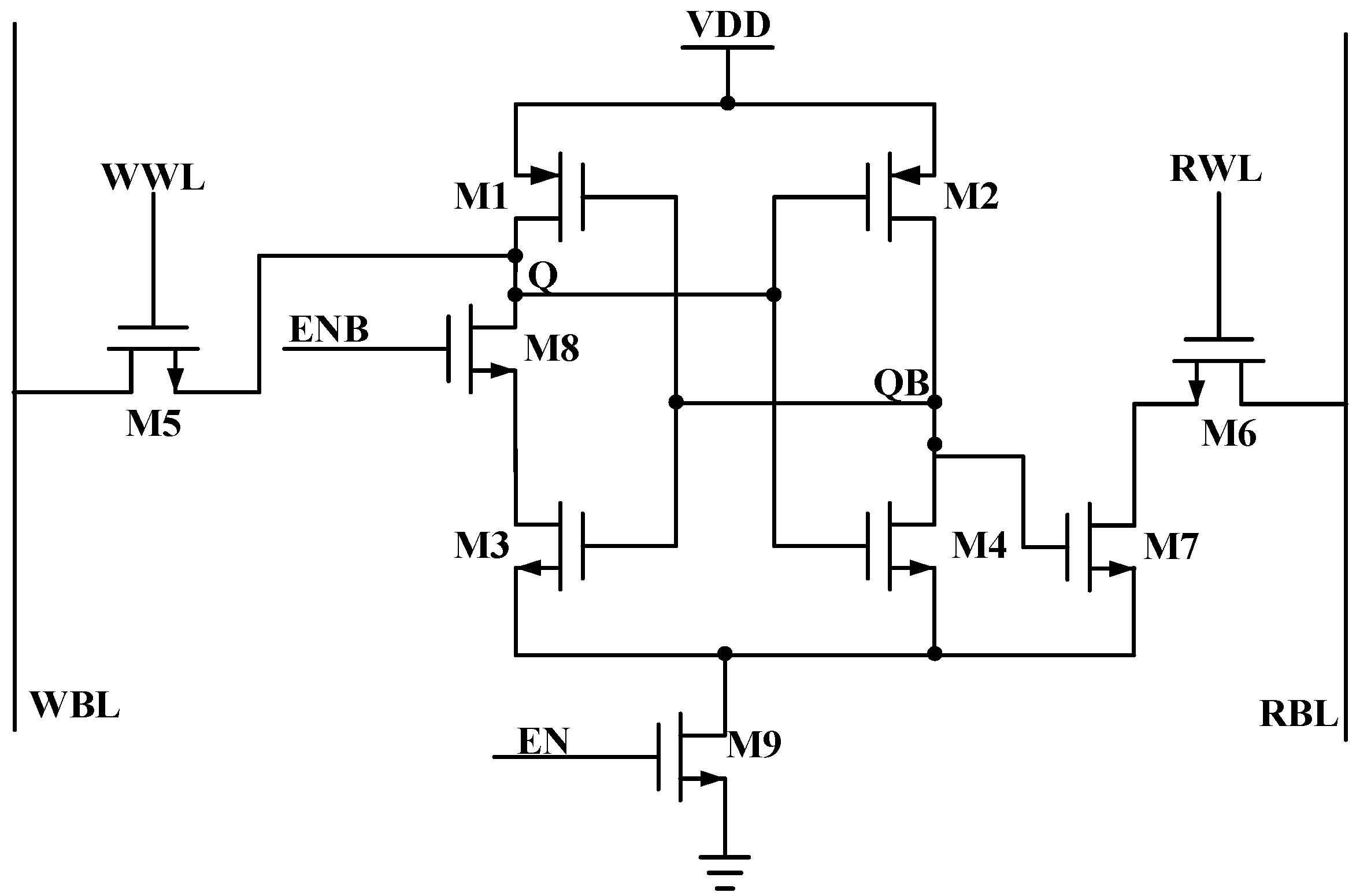
A novel read/write-decoupled SRAM cell based on CNTFET is proposed in this paper, as shown in
Figure 4. The novel cell has the advantages of low power consumption, high storage density, and high stability. The cell shown in
Figure 4 does not include a path between the pull-up and the pull-down transistors, thereby enabling all transistors to operate at minimal size and achieving a significant reduction in cell area. Compared with the conventional 6T SRAM cell, the 9T SRAM cell has three more transistors, namely, M7, M8, and M9. The gate of M7 is connected to the storage node QB, which can separate the storage node with an external circuit and improve the stability of the memory cell. Transistor M8 is short when the circuit is in standby mode and maintains the memory cell in a cross-coupled feedback state. During the read/write state, transistor M8 turns off to cut off the feedback loop of the memory cell and enable more efficient data writing to the storage node. Transistor M9 decreases the leakage current when the circuit is in standby state.
The read/write timing of the proposed SRAM cell is shown in
Figure 5. When the write word line (WWL) is 1, the read word line (RWL) is 0, EN is 1, ENB is 0, and both M6 and M8 are turned off, while M5 and M9 are turned on, enabling direct data writing from the write bit line (WBL) to storage node Q. Conversely, when the WWL is 0, the RWL is 1, EN is 1, ENB is 0, and both M5 and M8 are turned off, while M6 and M9 are turned on. If the storage node Q is 0, QB is 1, and transistor M7 is turned on. As M6 is also turned on, a path from the read bit line (RBL) to the ground is formed, which lowers the RBL voltage. If the storage node Q is 1 and QB is 0, transistor M7 is turned off. The voltage of RBL remains the same as that in the precharge state. The readout data are held high after passing through the sense amplifier.
2.3. Sense Amplifier
The structure of the sense amplifier used in this study is shown in
Figure 6 [
14]. Before the read operation, the sense amplifier is in the precharge state, the value of the PRE signal is 1, PRE_BAR is 0, and EN is 0. Transistors M1 and M9 are turned on, and the precharging nodes are a and c, respectively. As the transmission gate formed by M10 and M11 remains conductive, the potentials of nodes a and b are equal, which are clamped to approximately 1/2 VDD. Meanwhile, transistor M13 turns on, pulling node d to the ground. The potential of node c is precharged to high due to the signal of node d propagating through the inverter composed of transistors M7 and M8. Consequently, the potential of DOUT is held high during the precharge state. During the read operation, the value of the PRE signal is 0, PRE_BAR is 1, and EN is 1. Transistors M1 and M9 are turned off, and the transmission gate formed by M10 and M11 is also turned off. For logic “0” detection, RBL starts to discharge, the potential of node b rapidly rises, M6 turns on, and node d is pulled up to high potential. The potential of node c is discharged to a low level due to the signal of node d propagating through the inverter composed of transistors M7 and M8. At the same time, transistor M12 turns on, and the potential of node d is pulled up again, forming a positive feedback loop to accelerate the sensing speed. For logic “1” detection, the potential of RBL remains unchanged, and there is no change in the potential of nodes a and b. Transistor M6 turns off, and node c remains in the same state as prior to the read operation, resulting in the high potential of node c.
2.4. Clock Gating
To reduce power consumption, clock gating was introduced to process the clock signal in this study. The use of clock gating can effectively reduce unnecessary flip and dynamic power consumption. The clock gating circuit encompasses AND-based clock gating, latch-based clock gating, and register-based clock gating [
15]. The AND-based clock gating is the simplest and most direct gated clock circuit, achieving the enabling and disabling of the clock signal through a logical AND operation between the gating signal and the clock signal. However, the AND gate may introduce additional propagation delay when the gating signal has a rapid transition rate, which may influence the timing and performance. The latch-based clock gating controls the clock signal propagation through the latch. Similarly, the register-based clock gating controls the propagation through the register. Compared with AND-based clock gating, the implementations of latch-based and register-based clock gating are more complex and require additional control logic. Furthermore, register-based clock gating may require more resource consumption.
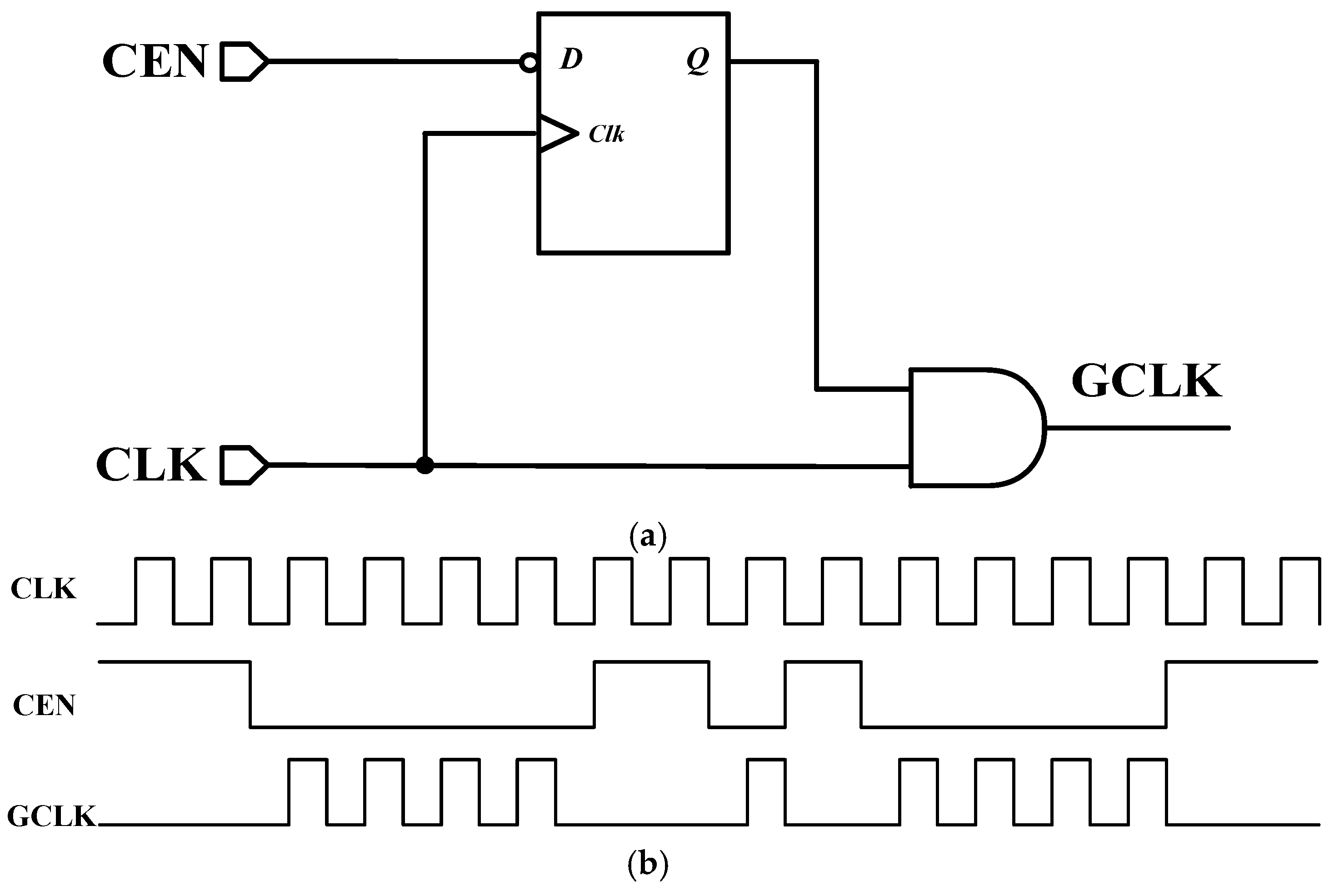
The latch-based clock gating is shown in
Figure 7. When CEN is held low, the clock propagation is permitted to ensure normal operation. Conversely, when CEN is held high, the clock propagation is prevented by the gating signal, achieving power consumption reduction.
3. Simulation Results
The proposed design was implemented by a silicon-based 55 nm and a carbon-based 500 nm process. Monolithic 3D (M3D) integration technology was applied to the carbon–silicon heterogeneous-integrated SRAM design. The M3D technology integrates silicon-based and carbon-based devices in a vertically stacked multilayer architecture, achieving hierarchical optimization of logic, memory, and interconnect functions [
16]. The key to M3D technology resides in utilizing complementary properties of silicon and carbon materials to transcend the physical limits of conventional 2D integration. Ref. [
17] implemented a monolithic three-dimensional heterogeneous integrated sensing–memory–compute system-on-chip. The work employed monolithic 3D integration technology to construct a four-layer vertically stacked structure, integrating over two million CNTFETs and one million resistive random-access memory (RRAM) cells. It represents the largest functional monolithic 3D system based on nanomaterials to date, showing the scalability of carbon nanotube monolithic 3D integration technology. In addition, researchers have proposed a fully carbon-based monolithic three-dimensional sensing system [
18]. The system features a CMOS voltage-controlled oscillator as the analog-to-digital conversion unit and a CNTFET-based multifunctional sensor as the sensing unit. Operating at 5 V supply voltage, the system achieved a concentration gradient response ranging from 780 MHz to 1.1 GHz, with a frequency response resolution of 2.75 MHz/ppm (1 ppm = 10–6). A Stanford University team employed monolithic three-dimensional integration technology to directly integrate a CNTFET-based computing layer onto the back end of line (BEOL) of a silicon imager, constructing a three-layer vertical structure that eliminates the conventional bottleneck of serial read–memory–compute operations and enables real-time pixel-level processing [
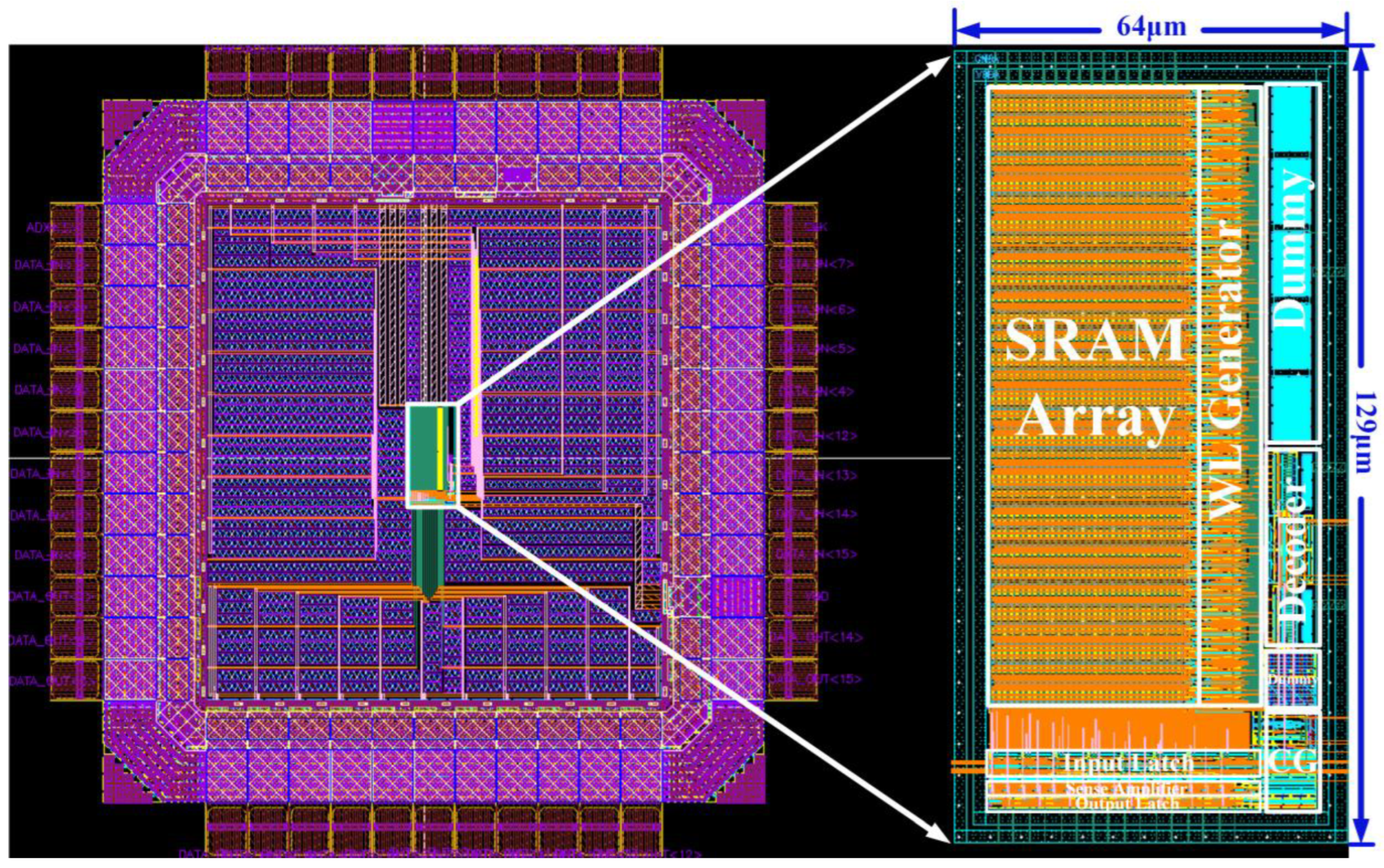
19]. This research indirectly demonstrates the reliability and feasibility of the carbon–silicon heterogeneous integrated SRAM technology proposed in this work. The layouts of silicon-based SRAM and carbon–silicon heterogeneous-integrated SRAM are shown in
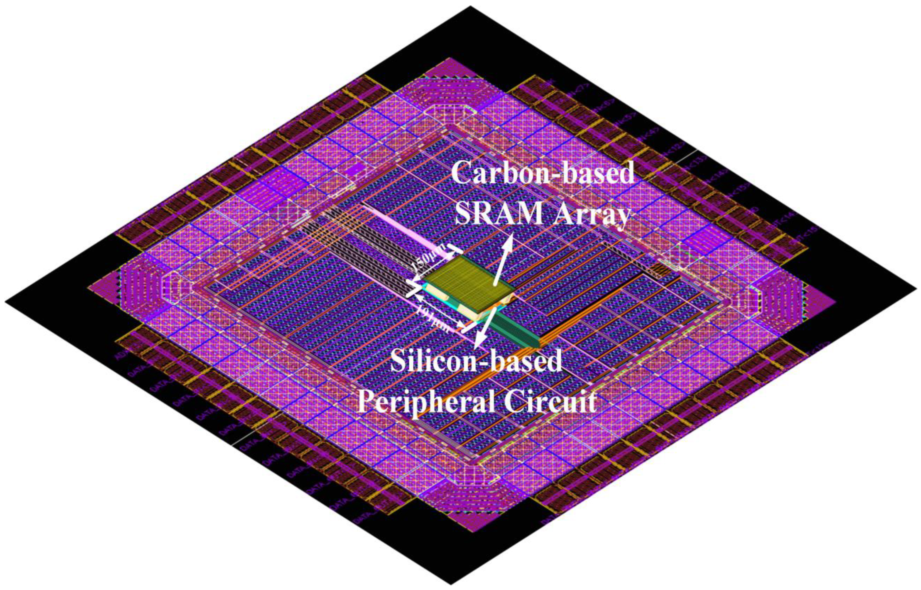
Figure 8 and
Figure 9, respectively. The active area of the silicon-based SRAM is 0.008256 mm
2, and the active area of the carbon–silicon heterogeneous-integrated SRAM is 0.02865 mm
2. As the proposed design was implemented by a silicon-based 55 nm process and a carbon-based 500 nm process, there is significant disparity in the feature sizes of the transistors. If transistors with comparable feature sizes are used, higher integration density can be achieved. The proposed design methodology can better demonstrate its area advantages under more advanced carbon-based technology nodes.
3.1. Simulation Results of Novel Cell
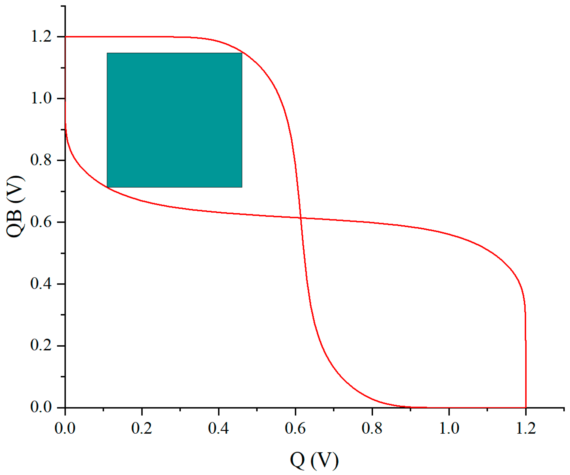
Static noise margin (SNM) is a key metric that evaluates the ability of a memory cell to resist external noise interference during standby mode. SNM represents the maximum DC noise voltage that a memory cell can withstand without inducing data flipping when read and write operations are not performed. The butterfly curve of the proposed carbon-based memory cell, depicted as the red curve, is shown in
Figure 10. The SNM is defined as the side length of the largest square in the butterfly curve, which is shown as the green square in
Figure 10. The SNM of the proposed 9T SRAM cell is 399.9 mV. A comparison of the SNM with other carbon-based SRAM cells is shown in
Table 1. Compared with 6T [
20], 8T [
21], 10T [
22], and 10T [
23] carbon-based designs, the SNM of the proposed carbon-based cell is higher by 33.3%, 22.14%, 23.72%, and 18.68%, respectively. Although the SNM of the proposed carbon-based cell is 0.58% smaller than that of 12T [
24], the proposed carbon-based cell achieves less area and higher integration density. The results show that the proposed carbon-based cell is feasible and has a superior ability to resist external noise interference.
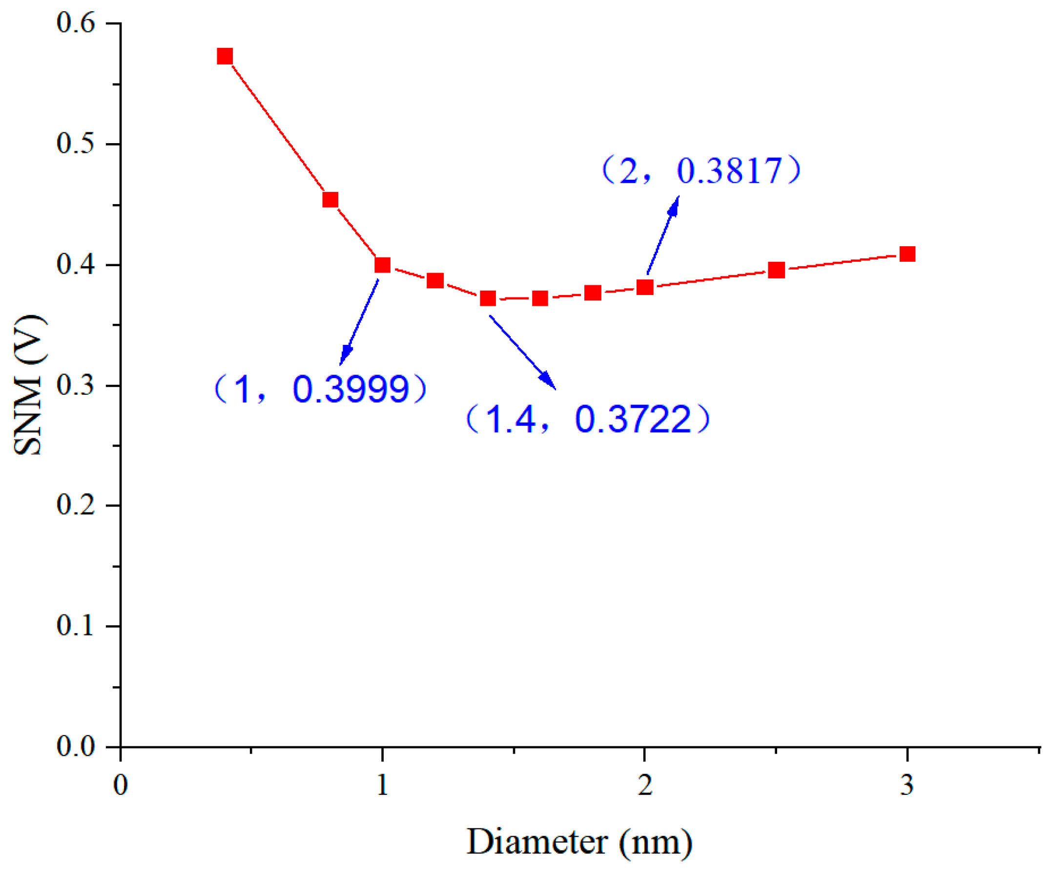
In carbon-based SRAM cells, the chiral vector of carbon nanotubes indirectly determines the SNM by its diameter, bandgap, and electrical properties. The VS-CNTFET model [
25] does not explicitly encompass the chiral vector. Instead, it utilizes the diameter as a core parameter. The recommended diameter range of the model is 1~2 nm. As shown in
Figure 11, the SNM of the proposed cell initially decreases and then gradually increases within the diameter range from 1 nm to 2 nm. When the diameter of carbon nanotubes is 1 nm, the SNM reaches the maximum of 399.9 mV. When the diameter exceeds the recommended range, the SNM increases significantly, approaching 600 mV. Although the diameter of carbon nanotubes exceeding the recommended diameter range can improve SNM, it may induce unpredictable issues such as increased power consumption and circuit function failure. Therefore, when using the VS-CNTFET model for circuit design, an appropriate diameter should be selected to ensure proper circuit operation.
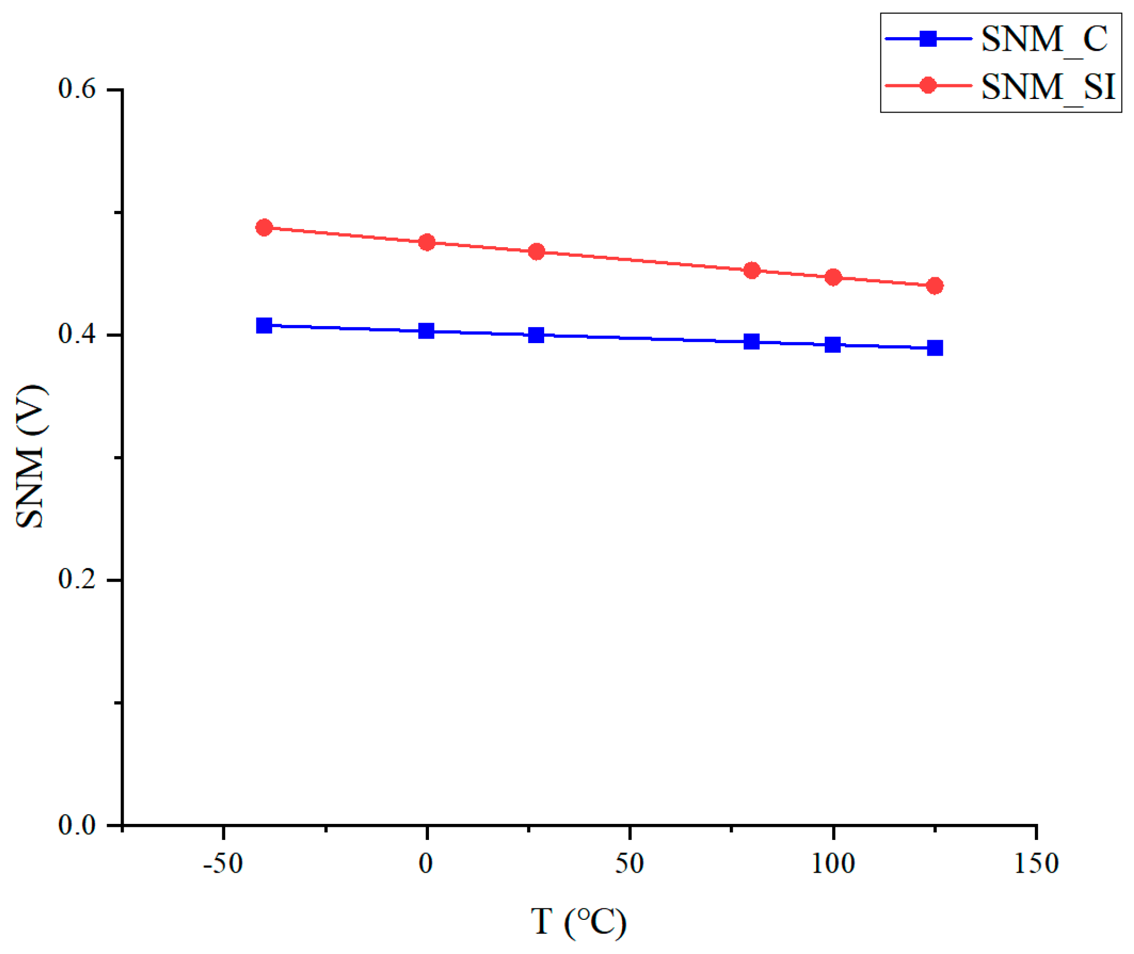
An analysis of SNM on both carbon-based 9T and silicon-based 9T SRAM cells at different temperatures was conducted. The result is shown in
Figure 12. Although the SNM of the silicon-based cell is higher than the carbon-based one of the same size, the carbon-based cell is less dependent on temperature, indicating that the carbon-based cell has superior temperature stability.
The power consumption of SRAM cells primarily consists of dynamic and static power consumption. Dynamic power consumption primarily consists of the charging and discharging consumption of bit lines and storage nodes, as well as the short-circuit power consumption generated by the simultaneous conduction of transistors during switching transients. Static power consumption primarily consists of the leakage power generated by the transistors when they are turned off. The power consumption of carbon-based, 2D material-based (2DM), and silicon-based SRAM cells is compared in
Table 2. Overall, the carbon-based SRAM cells exhibit superior low-power performance, and the carbon-based 9T cell proposed in this paper has lower static power consumption.
The read delay of SRAM cells primarily consists of the word line activation delay and the bit line discharge time (discharge to the trigger threshold of the sense amplifier). As the potential of RBL remains unchanged during read 1 (as discussed in
Section 2.3), only read 0 delay is performed. The read delay is defined as the time required for the RBL to discharge from precharge potential to ground potential. The write delay of SRAM cells primarily consists of the word line activation delay and the transition of the storage node. The read/write delays of carbon-based, 2D material-based, and silicon-based SRAM cells are compared in
Table 3. The results show that the carbon-based SRAM cells exhibit superior read/write performance, and the carbon-based 9T cell proposed in this paper has faster read/write speed.
3.2. Simulation Results of SRAM
The power consumption of SRAM circuits primarily consists of dynamic and static consumption. Dynamic power consumption is primarily generated by the SRAM during read/write operations or access switching. Static power consumption is primarily generated by the leakage current of transistors during the SRAM in standby state.
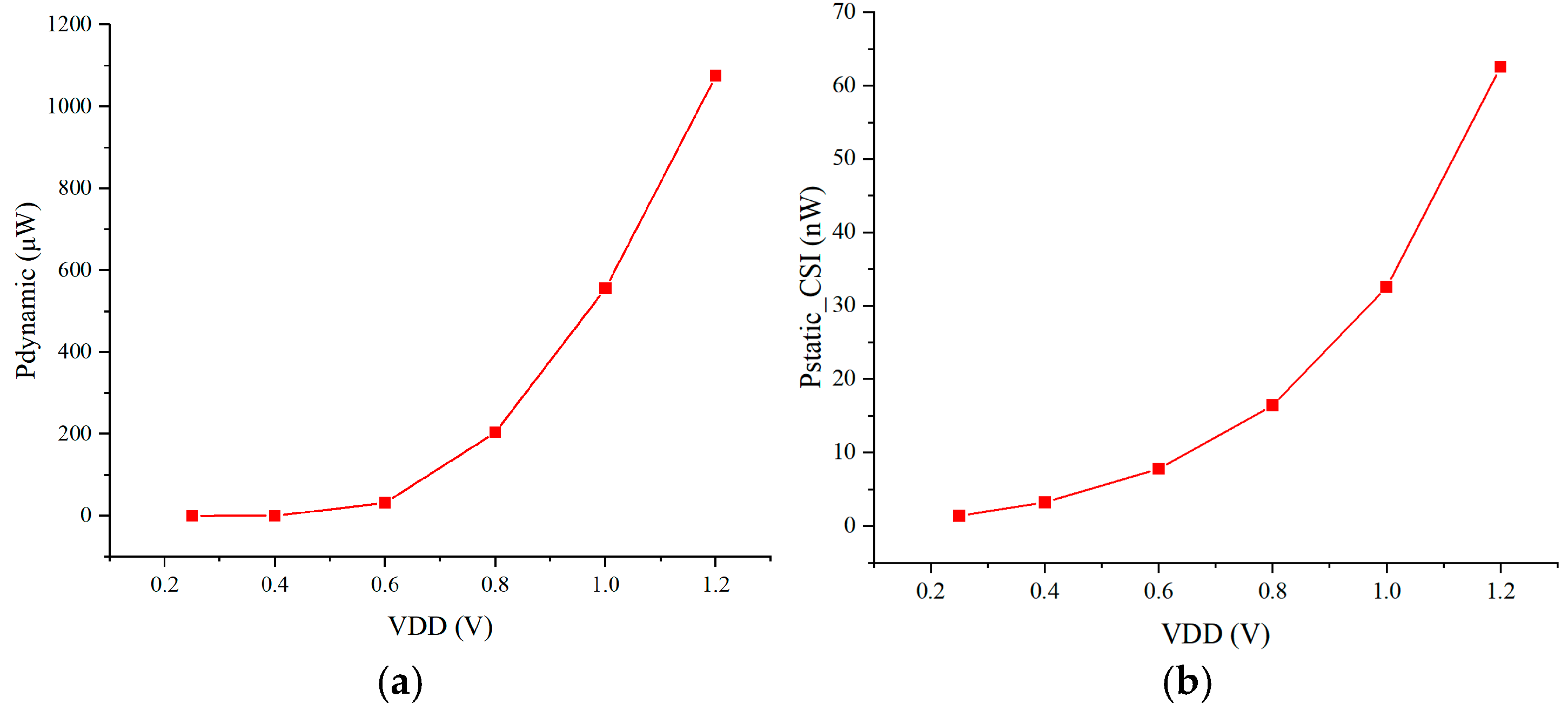
Figure 13 presents the dynamic power consumption (
Figure 13a) and static power consumption (
Figure 13b) of the carbon–silicon heterogeneous-integrated SRAM as functions of the supply voltage, ranging from 250 mV to 1.2 V. When the supply voltage is 1.2 V, the dynamic power consumption of the proposed SRAM is 1.07 mW and the static power consumption is 62.54 nW.
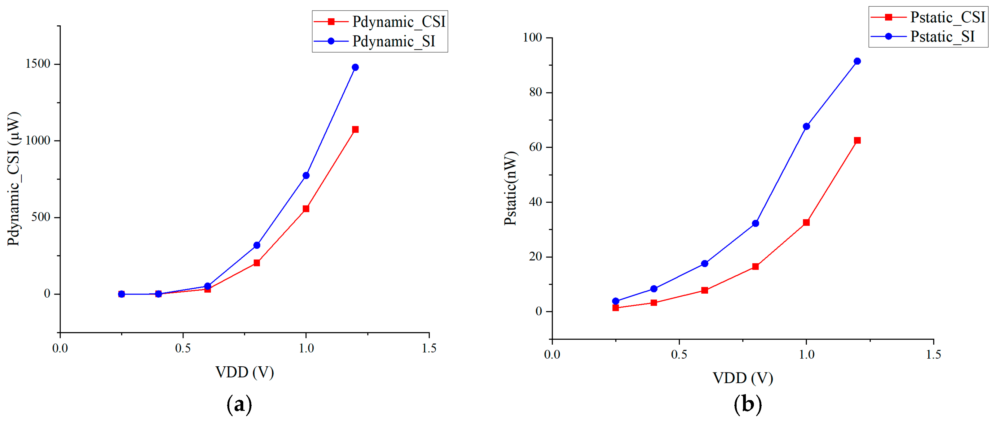
Figure 14 presents the power consumption of the carbon–silicon heterogeneous-integrated SRAM and silicon-based SRAM as functions of the supply voltage under identical capacity and circuit structure. As shown in
Figure 14, the power consumption of the carbon–silicon heterogeneous-integrated SRAM is lower than that of the silicon-based SRAM. The result is consistent with previous theories.
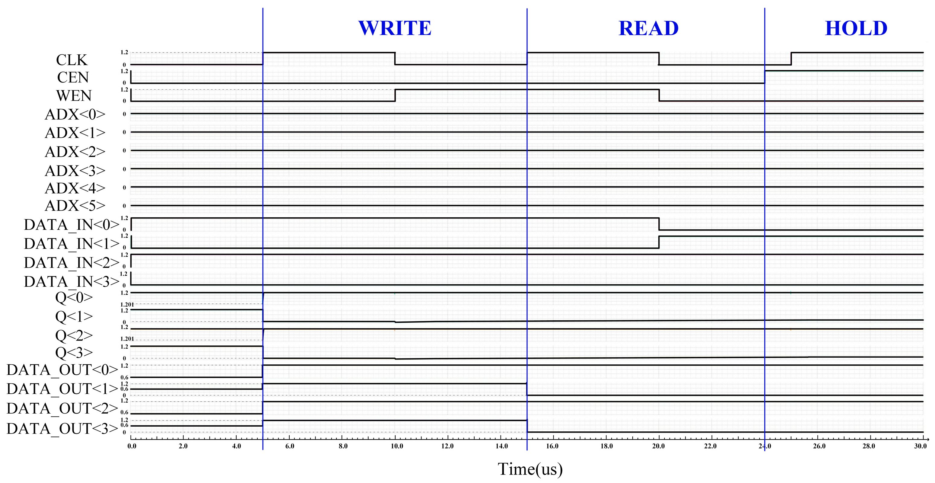
The timing of the proposed SRAM is shown in
Figure 15. When both CEN and WEN are pulled low, a write operation is triggered at the rising edge of CLK, and external data DATA_IN will be written into the storage node Q. When CEN is pulled low and WEN is high, a read operation is triggered at the rising edge of CLK, and the value of storage node Q will be read out through the sense amplifier. When the CEN is high, SRAM enters a standby mode, and the values of storage node Q and DATA_OUT remain unchanged.
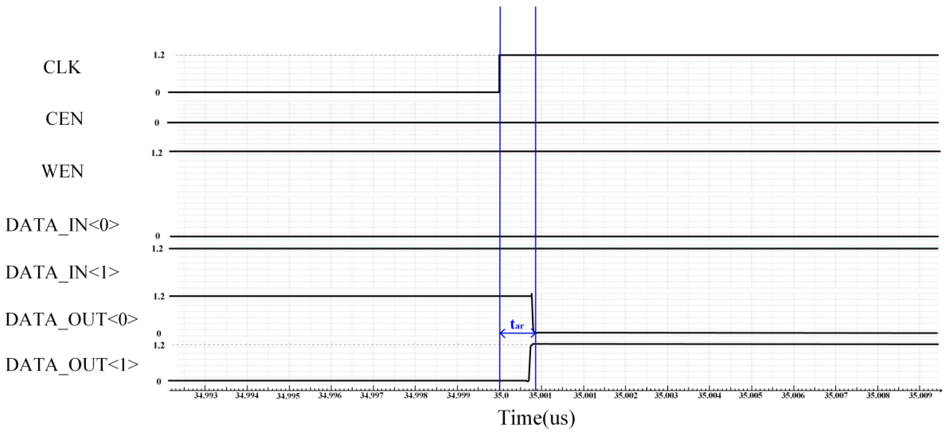
The access time of SRAM is defined as the total time required from receiving an access request to correctly reading out the data. It is a key metric that evaluates the performance of SRAM and directly affects the overall speed of the system. As shown in
Figure 16, the access time of the proposed SRAM is 872 ps.
The comparison results of this work with others are shown in
Table 4. The proposed SRAM achieves the lowest static power consumption due to the novel 9T cell, which can reduce leakage current during standby mode. Due to the superior performance of carbon nanotubes, such as high carrier mobility and low power characteristics, the carbon–silicon heterogeneous-integrated SRAM has lower power consumption and access time than the SRAM employing CMOS technology.
4. Conclusions
This paper proposes a low-power carbon–silicon heterogeneous-integrated SRAM. This SRAM was implemented by a silicon-based 55 nm process and a carbon-based 500 nm process, operating at 1.2 V supply voltage. The simulation results showed that the read delay of SRAM using a silicon-based 55 nm process was 886 ps, the static power consumption was 91.51 nW, and the dynamic power consumption was 1.48 mW. The SRAM with carbon–silicon heterogeneous-integrated technology achieved 1.58%, 31.66%, and 27.70% reductions in read delay (from 886 ps to 872 ps), static power consumption (from 91.51 nW to 62.54 nW), and dynamic power consumption (from 1.48 mW to 1.07 mW), respectively. For SRAMs with larger storage capacities, the design principle proposed in this work can reflect more significant power consumption advantages. As the storage array occupies over half of the total area in large-capacity SRAMs, the proposed memory cell can reduce the overall static power consumption. Furthermore, as the storage array is designed using carbon-based technology, CNTs inherently possess low-power characteristics, and the power consumption of SRAMs can be further reduced. In addition, with the adoption of more advanced carbon-based technology nodes in the future, the proposed carbon–silicon heterogeneous integration method can further highlight its integration advantages.
It is worth mentioning that CNTFETs still face technical limitations in manufacturing and integration. High surface roughness of the interlayer dielectric can lead to the embedding of nanoscale carbon nanotubes into irregular voids, thereby reducing their effective density and severely degrading the quality of source/drain contacts, which is detrimental to the performance of CNT transistors. Moreover, constrained by wafer thinning and bonding alignment processes, through-silicon via (TSV) technology struggles to match the high density of CNT devices, limiting the potential of 3D stacking. Compared with TSV-based 3D integration, monolithic 3D integrated circuits are fabricated sequentially from the substrate in the vertical direction, with multiple layers of active transistors and back-end-of-line interconnects. The density and dimensions of interlayer interconnects rely on advanced back-end processes, and alignment accuracy is determined by the lithography tool. Therefore, the monolithic 3D integration technology has a higher upper limit of interconnect density and offers greater scalability and potential. This work provides a novel pathway to overcome the performance limitations of silicon-based memory and lays the foundation for high-performance, low-power carbon-based memory designs in the future. Furthermore, it provides innovative methodologies for integrated circuit technologies in the post-Moore era.
