Article

Hash-Based Message Authentication Code with a Reverse Fuzzy Extractor for a CMOS Image Sensor †

Graduate School of Science and Engineering, Ritsumeikan University, 1-1-1 Nojihigashi, Kusatsu-shi 525-8577, Japan
*
Author to whom correspondence should be addressed.
This paper is an extended version of our paper published in Okura, S.; Ishikiy, R.; Takanoy, S.; Shirahatay, M.; Kubotay, T.; Shiozakiy, M.; Ishikawa, K.; Takayanagi, I.; Fujinoy, T. A 2-Mpixel CMOS Image Sensor with Device Authentication and Encryption Key Generation Based on Physically Unclonable Function. In Proceedings of the 2019 International Image Sensor Workshop (IISW), Snowbird, UT, USA, 23–27 June 2019.
Electronics 2025, 14(10), 1971; https://doi.org/10.3390/electronics14101971
Submission received: 10 March 2025 / Revised: 20 April 2025 / Accepted: 1 May 2025 / Published: 12 May 2025
(This article belongs to the Section Networks)

Abstract

:
The MIPI (Mobile Industry Processor Interface) Alliance provides a security framework for in-vehicle network connections between sensors and processing electronic control units (ECUs). One approach within this framework is data integrity verification for sensors with limited hardware resources. In this paper, the security risks associated with image sensor data are described. Adversarial examples (AEs) targeting the MIPI interface can induce misclassification, making image data integrity verification essential. A CMOS image sensor with a message authentication code (CIS-MAC) is then proposed as a defense mechanism starting from the image sensor to protect image data from malicious manipulations, such as AE attacks. Evaluation results of the physically unclonable function (PUF) response and random number, which are utilized for generating the cryptographic key and MAC tag, are presented using a 2 Mpixel CMOS image sensor. The area of the CIS-MAC circuit is estimated based on a Verilog HDL design and synthesis using a 0.18 μm CMOS process. Various hash topologies are evaluated to select a hash function suitable for key generation and MAC tag generation within the CMOS image sensor. The estimated area of the CIS-MAC circuit is 67 kGE and 0.86 mm 2 , demonstrating feasibility for implementation in a CMOS image sensor typically fabricated using analog process technology.

1. Introduction

To guarantee the success of the Internet of Things (IoT), information security is required. For this purpose, security functionalities such as authentication of system components, data integrity protection, and data encryption can be utilized according to required security level.
The Mobile Industry Processor Interface (MIPI) Alliance has established a security framework to safeguard long-range, in-vehicle network connections between image sensors and their corresponding processing electronic control units (ECUs). Image sensors play crucial roles in advanced driver assistance systems (ADASs) and autonomous driving systems (ADSs). To ensure security, it is vital to protect the data transmitted by these sensors against threats such as the installation of unauthorized components, malicious alterations of sensor data, and potential privacy breaches due to unauthorized access. However, approaches integrated into image sensors for the purpose of safeguarding the captured data from such threats have not yet been thoroughly addressed. Therefore, the Physically Unclonable Function (PUF) [1,2,3,4,5] is rapidly being developed as a lightweight on-chip authentication solution to address security concerns in IoT. Static Random Access Memory (SRAM) PUFs have been extensively studied [6]. Additionally, non-volatile Resistive Random Access Memory (RRAM) PUFs have attracted significant research interest due to their superior reconfigurability [7]. For a CMOS image sensor which does not employ large RAM cells, the CIS with a PUF (CIS–PUF) [5,8] presents another notable PUF with small in-pixel overhead, where pixel-to-pixel fixed pattern noise (PPFPN) is utilized to generate unique fingerprint pattern from a large number of pixels. In this paper, we propose a CMOS image sensor integrated with a Hash-based Message Authentication Code (HMAC) as a defense mechanism beginning at the image sensor level. This security is implemented at the pixel level, thus ensuring the scalability of the framework. Protection is guaranteed from the origin of the sensor data within the sensor device to its final destination in the system-on-chip (SoC) device. Sensor application developers are tasked with balancing the necessary security measures with the processing efficiency, implementation complexity, thermal management, and power consumption of the sensor system. The MIPI framework specifies two ciphersuites: one optimized for efficiency and the other for performance. The “efficiency” ciphersuite ensures the integrity of data using AES–CMAC (without encryption), and is intended for sensors with constrained hardware resources. The “performance” ciphersuite provides data integrity using AES–GMAC, along with optional AES–CTR encryption, and is designed for sensors equipped with dedicated hardware support. This framework is computationally efficient and can also be applied to other use-cases that utilize image sensors for machine vision applications. In particular, the deployment of image sensors in safety-critical applications is expected to increase as the development of the IoT ecosystem progresses.
For the “efficiency” ciphersuite, the PUF serves as a unique identifier (ID) and cryptographic key for a device, leveraging the physical variations inherent to the manufacturing process. The strong dependence of PUF on internal physical parameters makes them highly tamper-evident IDs and key storage solutions that do not require non-volatile memory (NVM). Thus, PUF provide a secure foundation starting from the data source, preventing attackers from exploiting vulnerabilities in sensor networks. To ensure the security of image information, we previously proposed a 2 Mpixel, 12 bit CIS–PUF [8], in which the pixel-to-pixel fixed pattern noise (PPFPN) is utilized as the PUF ID for each device. CIS–PUF-based device authentication is achieved through a challenge–response (CR) authentication scheme, which consists of two phases: enrollment and verification. During the enrollment phase, the whole PUF ID bits derived from the pixel array are recorded by the verifier. In the verification phase, the verifier issues a challenge, which is a randomly selected pixel address. The CIS then responds with the PUF ID string corresponding to the verifier’s challenge. As the verifier issues a different challenge for each authentication session, knowledge of a previous correct response does not benefit an attacker. Beyond device authentication, PUF can also be utilized to generate cryptographic keys for the “efficiency” ciphersuite, such as for data integrity verification, where the key is effectively bound to the CIS. The cryptographic key, which is initially generated during enrollment, is securely recorded by the ECUs. The CIS–PUF regenerates the key on demand, which is required for the message authentication code (MAC). To generate cryptographic keys while mitigating the noise present in PUF response measurements, post-processing is necessary. For CIS–PUF, we have further proposed a fuzzy extractor-based dynamic soft-decision error correction mechanism, which achieves high error correction capability with minimal circuit overhead [9].
Our contribution is summarized as follows:
  • A CMOS Image Sensor with a Message Authentication Code (CIS-MAC) is proposed.
  • The evaluation results of the responses of the physically Unclonable Function (PUF) and the random numbers used to generate cryptographic keys and MAC tags are presented.
  • The integrity and authenticity of image protection technology are discussed.
  • Feasibility study for a small area implementation of CIS-MAC is performed.
In this paper, the security risks for image sensor data are first described, followed by the proposal of a CMOS image sensor with message authentication code (CIS–MAC) as a countermeasure. In Section 2, adversarial examples (AEs) are identified as a security risk for image sensor data. As AE attacks targeting the MIPI can induce misclassification, verifying the integrity of the image data is necessary. In Section 3, a CIS–MAC scheme that starts from the image sensor is proposed as a defense mechanism to protect image data against malicious manipulations, such as AE attacks. Evaluation results of the physically unclonable function (PUF) response and random number, which are utilized to generate the cryptographic key and MAC tag, are presented for a 2 Mpixel CMOS image sensor. In Section 4, the area of the CIS–MAC circuit is estimated based on a Verilog HDL design and synthesis using a 0.18 µ m CMOS process. Furthermore, various Hash topologies are evaluated to select a Hash function which is suitable for key and MAC tag generation in the CMOS image sensor.

2. Security Risks for Image Sensor Data

In a standard image recognition system [10,11,12,13], image data collected by an image sensor are sent to a host device, which then analyzes the data using AI. Ensuring the trustworthiness of the data from the image sensor and the analysis results is crucial for the secure use of the system. Figure 1 depicts the adversary’s attack scenario. Consider a system where image data captured by the image sensor are transmitted to the host device via MIPI, with the AI model on the host device performing image classification. The adversary seeks to cause misclassification in the AI model by executing a backdoor attack, which involves creating a backdoor model and manipulating the captured images. A real-world example of a threat has been reported, where an attack targets the mobile industry processor interface (MIPI)—the image sensor interface that transmits image data from the image sensor to the host device. This attack can be executed using a small attack device which is capable of injecting fault signals; for instance, in the context of car-sharing services, the attacker could potentially install the attack device within the vehicle. Invasive attacks, such as fault attacks [14], which involve physically injecting electrical faults into the MIPI to manipulate image data, and bypass attacks [15], which digitally alter image data by transmitting and receiving data through an attacking device, have been reported. Non-invasive attacks, such as electromagnetic interference (EMI) attacks [16] on MIPI, have also been documented. These tampering methods can be exploited to create adversarial examples [17,18] and backdoor attacks [19,20], ultimately leading to misclassification in AI classification outcomes. In the case of adversarial examples, model misclassification occurs by pre-computing the method to tamper with the entire image. In contrast, during a backdoor attack, the adversary can implant a backdoor model within the host device to cause misclassification when a specific trigger mark is present. The misclassification is then induced by placing the trigger mark at a particular location within the input image [14,21]. Although backdoor attacked images may appear to be visibly corrupted and could be recognized as altered by human observers, most traffic sign recognition systems do not display captured images when notifying drivers about detected traffic signs [22]. As a result, drivers are unlikely to be aware of the attack, significantly increasing its potential impact.
Using the German Traffic Sign Recognition Benchmark (GTSRB) [23] as the dataset and the VGG11 model [24] as the victim DNN model, we simulated how an attacker could use a backdoor attack to induce misclassification in the AI model. The model accuracy on the clean test dataset was 96%. The attack procedure is described as follows:
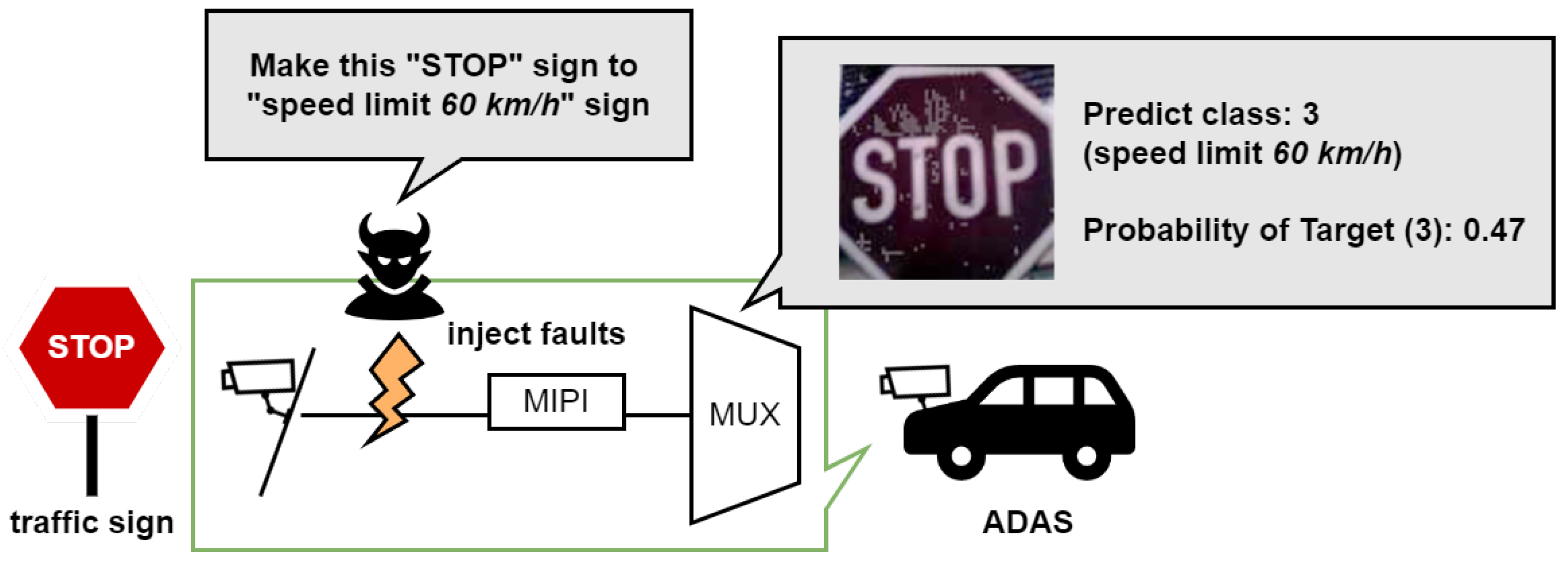
  • The attacker first pre-obtains a target image (e.g., a traffic sign) from the victim system. This image is used to pre-compute the perturbations used in the AE.
  • The attacker then connects an attack device to the victim system, which is capable of generating the pre-computed perturbations to implement a fault injection attack.
  • The AE is triggered only when the target traffic sign is captured, at which time the attack device continuously adds perturbations to the captured image by injecting fault signals into the image sensor interface.
Victim images belonging to class 14 (STOP) were selected, and the target class for misclassification was set to class 3 (speed limit 60 km/h). In this way, a fault injection attack was performed on the MIPI when the target pixel signal was transmitted. For 50 images acquired under fault injection, the attack success rate was 100% for target class 3. This result suggests that the integrity of the image data should be verified in order to prevent misclassification due to fault injection attacks against the MIPI.

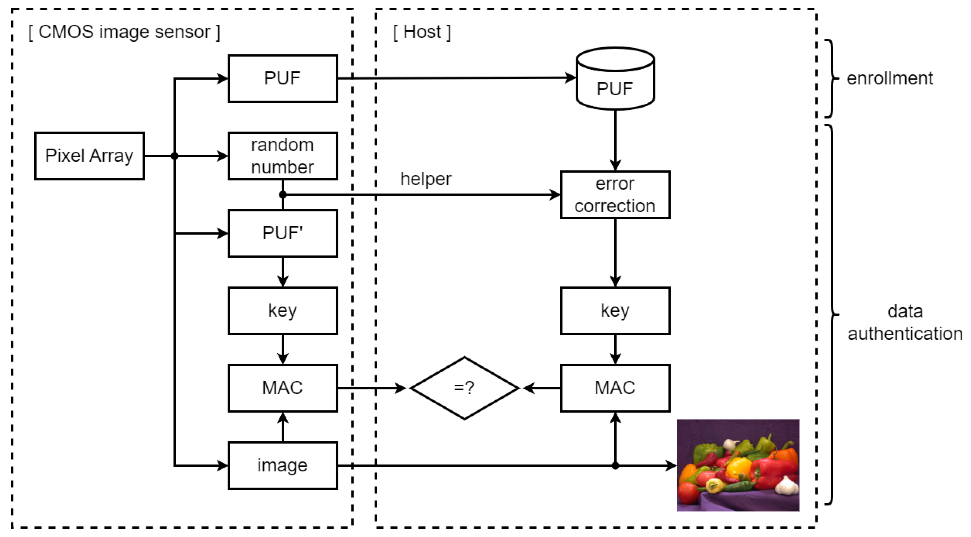
3. Overview of Message Authentication from CMOS Image Sensor to Host Device

In order to protect image data from malicious manipulations, including AE attacks, by employing a defense mechanism that originates at the image sensor, we propose a Hash-based message authentication scheme for a CMOS image sensor, as depicted in Figure 2. Not only does the image sensor generate imaging data, but it also produces a secret cryptographic key for the MAC tag. This cryptographic key is derived from a response of a Physically Unclonable Function (PUF) that exploits the inherent physical variations in the manufacturing process. During the authentication phase, the regenerated PUF response, denoted as P U F , exhibits a slight deviation from the reference response P U F obtained during the enrollment phase due to temporal noise. To mitigate this issue, helper data, encoded from the regenerated response P U F and a random number, are also employed for error correction. The reverse fuzzy extractor scheme [25,26] enables the execution of complex error decoding on the host device, which typically offers greater processing capability compared to the image sensor that is fabricated using analog process technology. The host device employs the helper data to correct the reference value P U F stored in its secure memory, thereby reproducing the cryptographic key from the noisy PUF response P U F . It subsequently generates a MAC tag using both the reproduced cryptographic key and the received image data. Finally, the host device verifies data integrity by comparing the MAC tags. If an attacker alters the device or modifies the image, the resulting compromise of data integrity leads to an authentication error.

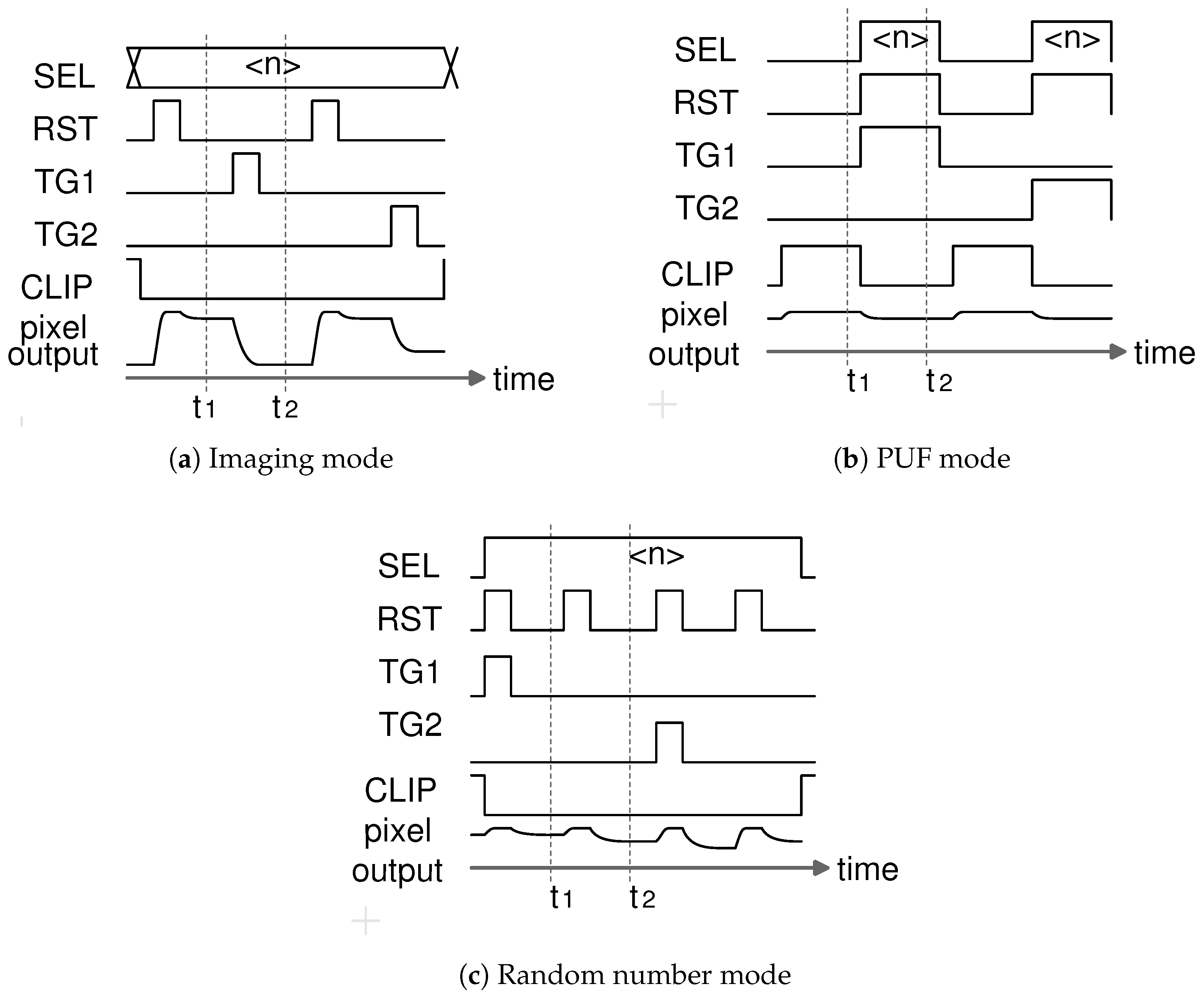
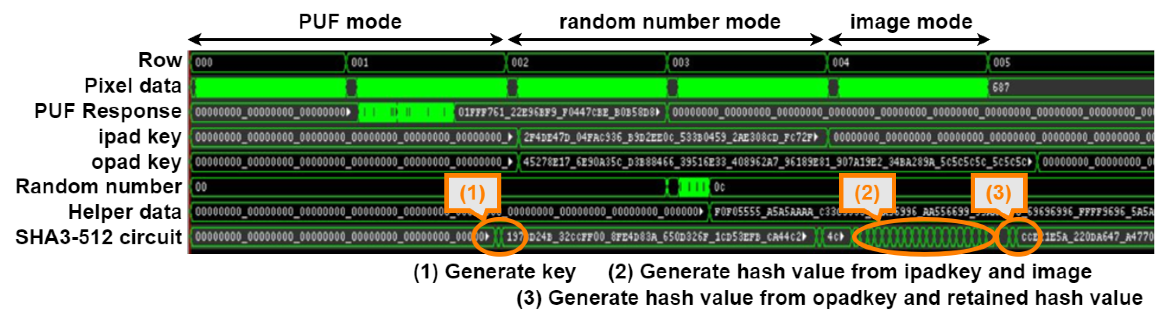
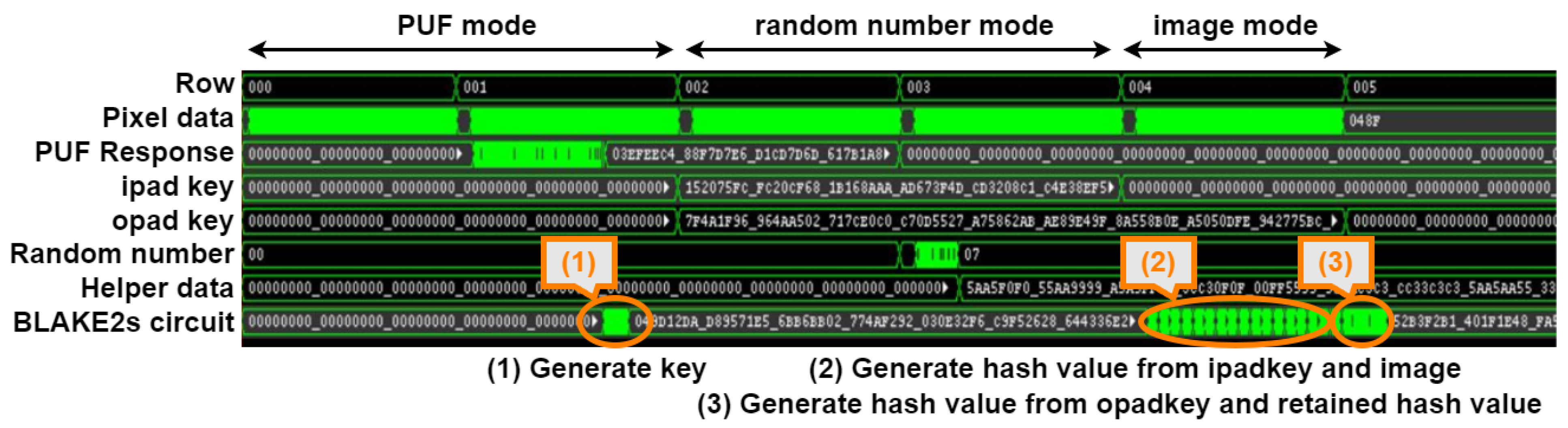
3.1. PUF Response and Random Number

We conducted an evaluation of a CMOS image sensor chip to assess its performance in generating both a PUF response and random numbers. Figure 3 depicts the evaluation environment, wherein a 2 Mpixel CMOS image sensor provided by Brillnics was employed as the device under test (DUT). Subsequently, the raw PUF data and raw random data were read out and processed on a PC to generate the PUF response and random number.
Figure 4 provides block diagrams showing an overview of the CMOS image sensor chip and a column readout circuit.
The pixel array consists of numerous pixels. A timing generator controls the vertical scanner that drives these pixels, while control registers toggle the pixel operation mode between imaging, PUF, and random number modes. The column readout circuit processes the pixel output voltage, generates a digital output that is subsequently transmitted to a signal processing circuit. Representative timing diagrams are presented in Figure 5 [27].
The readout signals under each operation mode are summarized in Table 1.
In the imaging mode, as depicted in Figure 5a, the reset and signal levels of a selected n th row pixel are read at t 1 and t 2 , respectively. After correlated double sampling (CDS) is performed by the column amplifier (AMP), the threshold voltage (Vth) of the SF transistor, along with the kTC noise, is canceled.
In the PUF mode, as shown in Figure 5b, the readout signals at t 1 and t 2 are used to derive the difference in output level between the clip-transistor M 0 and the SF in the n th row. Differential double sampling (DDS) is executed in the column amplifier (AMP) to capture the raw PUF data, which include both the V th variation and temporal noise. The V th variation is approximately 100 mV pp , a value attributed to the small size of the source-follower (SF) transistor, which is minimized to maximize the fill factor of the photodiodes (PD1 and PD2). In PUF mode, both the threshold voltage ( V th ) of the SF transistor and the kTC noise are read out, since the kTC noise is not canceled. However, in this scenario, the raw PUF data are predominantly influenced by the fixed V th variation rather than by the temporal noise, which is approximately 10 mV pp . A PUF response bit is assigned a value of either 1 or 0 through a comparison of the raw PUF data obtained from vertically adjacent shared pixels. The comparison between these vertically adjacent pixels eliminates the column fixed pattern noise (FPN), thereby enhancing the uniqueness of the PUF response [28], since the raw PUF data also include column FPN caused by variations in M 0 and the bias current I d .
To reliably generate the cryptographic key for the MAC tag, it is essential that the PUF response exhibits both high repeatability and uniqueness.
During the random number mode, as depicted in Figure 5c, the floating diffusion (FD) node is reset prior to both t 1 and t 2 . After the DDS is performed, the uncorrelated FD reset noise is read out, thereby removing both the optical signal integrated in PD1 and the threshold voltage of the SF transistor. The FD reset noise exhibits a normal distribution, with the FD capacitance C FD being approximately 1 fF and the FD reset noise (given by 2 k T / C F D ) measuring 2.9 mV at 1 σ . The least significant bit (LSB) of the A/D converter (ADC) output is employed as a raw random number bit, as the probability of “0” or “1” in the LSB is expected to be close to 50%; however, the non-linearity of the ADC introduces a bias in this probability. This probability bias can be mitigated by taking the XOR of multiple raw random number bits [29]. Furthermore, the randomness and unpredictability of the random number are crucial for concealing the P U F within the helper data employed for error correction.

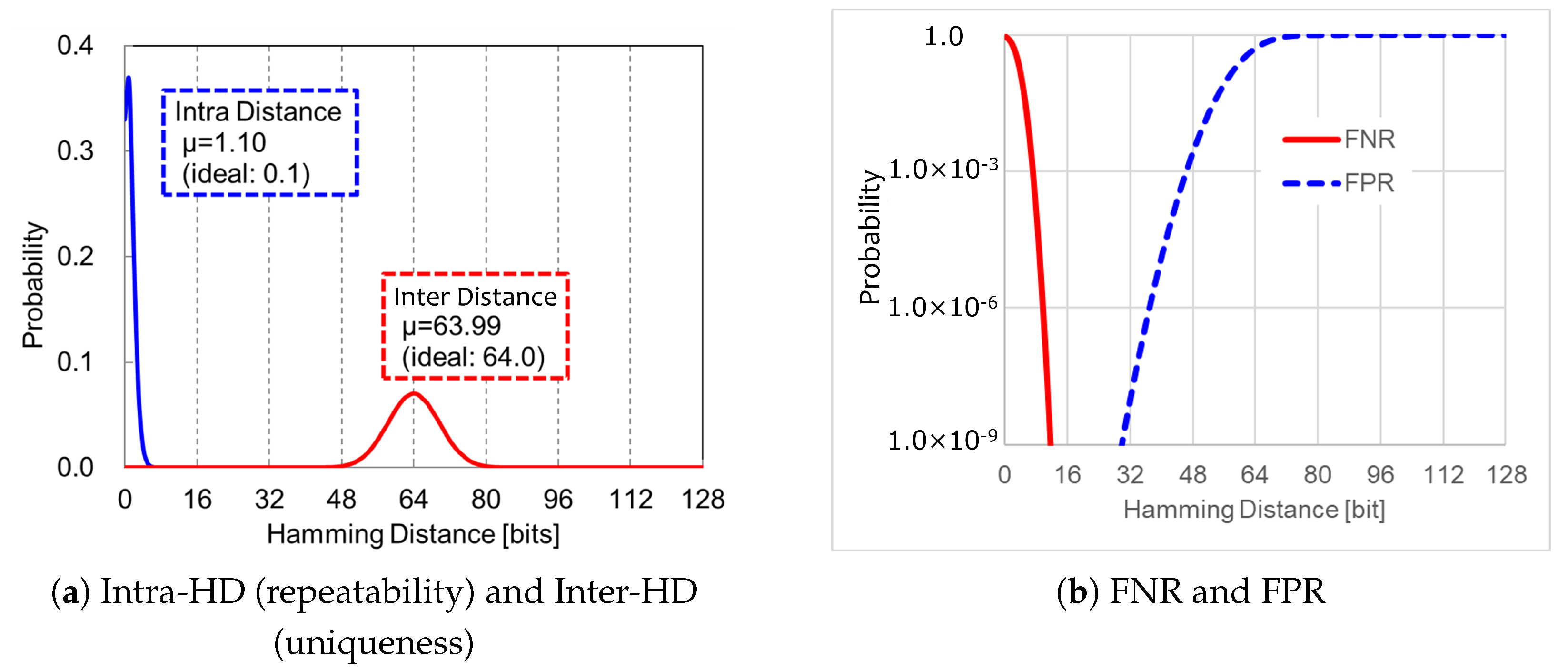
3.1.1. Evaluation of PUF Response

The PUF response is evaluated using the Hamming distance (HD), as shown in Figure 6, where the PUF ID length is 128 bits.
Figure 6a illustrates the Intra-HD and Inter-HD metrics [8]. The Intra-HD, derived from a single device, is influenced by temporal noise and indicates the repeatability of the response; meanwhile, the Inter-HD, measured across different devices, reflects the uniqueness of the response, ideally achieving a value of 50% (64 bits). For instance, 100 frames of PPFPN data are captured from 15 CISs and subsequently averaged to minimize the effect of random noise. The bit difference observed between two of the 15 devices is attributable to device-to-device mismatches. The distributions of the Intra-HD and Inter-HD do not overlap with each other. Both metrics were fitted to binomial distributions, and the false-negative rate (FNR) and false-positive rate (FPR) were computed using the cumulative distribution function, as illustrated in Figure 6b. For any given device, the probability that the Hamming distance (Intra-HD) exceeds 0 bits is 100%. Moreover, the probability that the Hamming distance exceeds 10% (i.e., 12/128 bits) is less than 1 × 10 9 . This observation indicates that simple error correction is sufficient for IoT applications. Meanwhile, the probability that the Hamming distance between different devices (Inter-HD) is below 128 bits is 100%, and the probability that it is under 22% (i.e., 29/128 bits) is less than 1 × 10 9 . The repeatability was additionally evaluated under voltage and temperature (VT) variations, with the supply voltage ranging from 2.6 V to 3.0 V and the ambient temperature spanning from 0 °C to 60 °C. At 2.6 V and 60 °C, the worst repeatability was observed, with a Hamming distance of 1.62 % ( 2.07 /128 bit). This indicates that the cryptographic key generated from the PUF response will be unique with high confidence and exhibit sufficient reproducibility of random noise even under severe conditions.

3.1.2. Evaluation of Random Number

To confirm the randomness of the CMOS image sensor’s output in random number mode, the entropy was estimated using the NIST SP 800–90B test [30]. Designed to evaluate the quality of entropy sources, this test employs 10 distinct entropy estimators. The raw random number data were captured over a length of 207 Mbit for entropy estimation. To mitigate the probability bias of “0” s and “1” s, between 0 and 3 rounds of XOR operations were applied to the raw random number bits as a post-processing step. The estimated minimum entropy, which is ideally equal to 1.0 under conditions of true randomness, is summarized in Table 2.
It can be seen that the minimum entropy improved as the number of XOR operations applied to the raw random number data increased. Table 3 presents detailed results of the random number tests conducted using NIST 800–22 for two cases: (A) XOR ×0 and (B) XOR ×3. The average p-value significantly improved with the application of 3 rounds of XOR operations, and the number of passed random number sequences also increased substantially. When XOR ×3 was applied, the generated random numbers exhibited high randomness, making them suitable for obscuring the PUF response in the helper data.

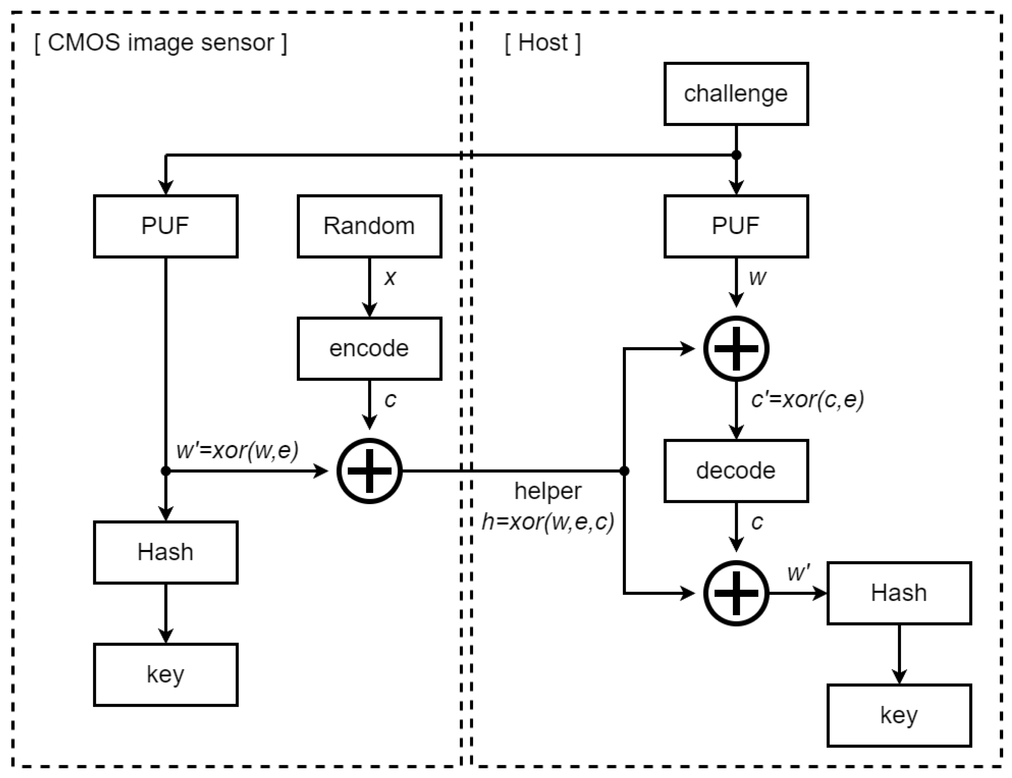
3.2. Key Generation Circuit

Figure 7 shows a block diagram of the key generation circuit used for the MAC tag based on the reverse fuzzy extractor approach [25], which allows for extremely lightweight implementations on resource-constrained CMOS image sensors.
The host device stores the PUF responses generated by the CMOS image sensor during the initial enrollment phase in its secure memory. When the user changes the device, the newly generated PUF response is stored in the secure memory once again. During the message authentication phase, the CMOS image sensor operates in PUF mode, and a PUF response w is measured for a given challenge. For enhanced security, the cryptographic key is derived by hashing the response w , ensuring that the raw PUF data are never stored in the non-secure memory of the CMOS image sensor throughout the message authentication process. Then, the CMOS image sensor is configured to operate in random number mode, and a random number x is subsequently read out. The random number x is encoded into c using an error-correcting code, and the helper data h are computed based on c and w . Meanwhile, the host device retrieves the PUF response w for the same challenge from its secure memory. Due to temporal noise e, the reference response w may not exactly match the regenerated w . Nonetheless, the reproduction procedure is capable of recovering the MAC key using the helper data h. The error-correcting code is capable of recovering the code c by decoding the XOR of w and h. The secret w is then retrieved by applying XOR to the recovered c with the helper data h, thereby enabling the MAC key to be produced in the host device. The random x must be unpredictable to ensure that the cryptographic key remains secure, since a predicted x combined with the public helper data h could expose the response w . This reverse fuzzy extractor approach eliminates the need for a memory circuit for the helper data in the CMOS image sensor, requiring only a logic circuit for error correction and Hashing.
The key extraction and recovery processes were simulated 620 × 10 3 times using the measured PUF response. We used the Reed–Muller (RM) code, which is frequently employed in communications applications. RM codes offer relatively high error correction performance and are easy to decode. In the fuzzy extractor, this code was applied as the error correction code [31,32]. In particular, RM(16,5,8) is more redundant than RM(8,4,4), but provides better error correction capability. With RM(8,4,4), key recovery failed 476 times, resulting in an error rate of only 0.077%. With the more redundant RM(16,5,8), every key recovery attempt was successful, and the error rate was less than 0.00017%, considering the finite number of key recovery operations.

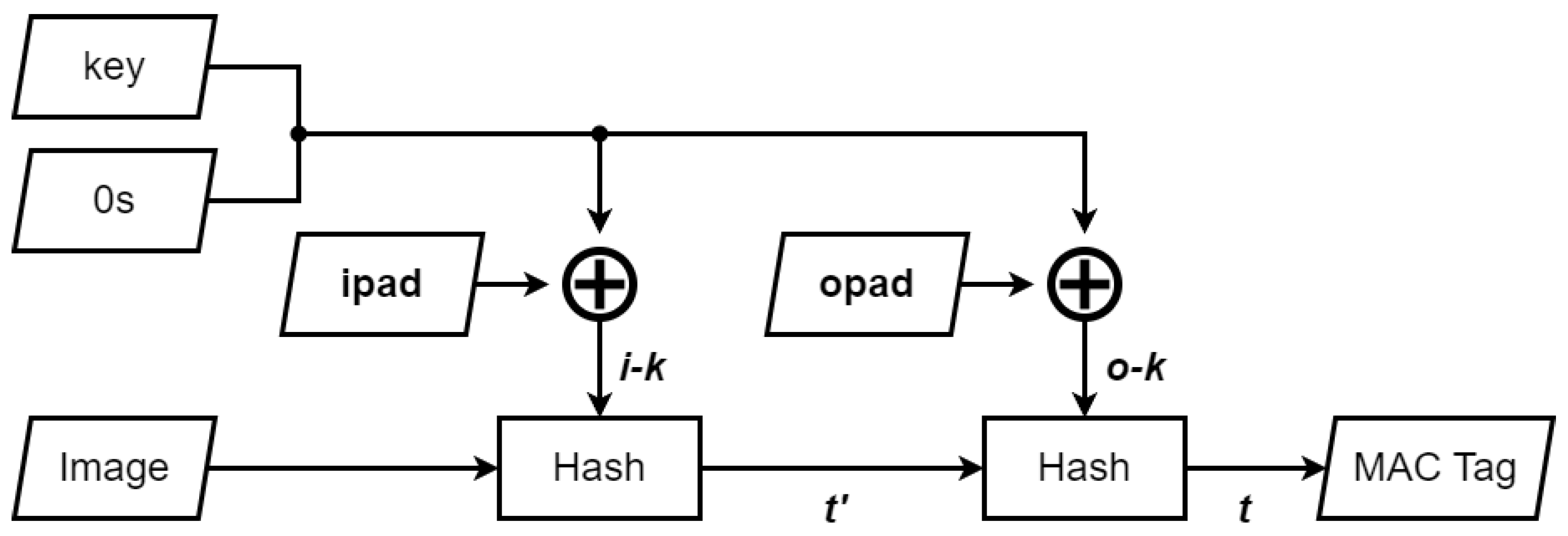
3.3. MAC Tag Generation Module

There are various implementations of MAC, and one approach that employs a Hash function to implement MAC is known as the Hash-based Message Authentication Code (HMAC) method [33]. HMAC, defined as a U.S. standard by NIST, is widely adopted in cryptographic applications. Rather than prescribing a specific Hash function, HMAC permits the use of any Hash function. An overview of HMAC is provided in Figure 8.
First, zero-padding is applied to the key so that the size of the input key becomes equal to the block length of the Hash function. An ipad key i-k is subsequently generated by XORing the padded key with a bit string called ‘ipad’, which is formed by repeating the bit string ‘00110110’ until it matches the block length of the Hash function. The input message is concatenated with the key i-k and then fed into the Hash function, resulting in the generation of an intermediate Hash tag t . However, since this intermediate Hash tag t is vulnerable to tampering and spoofing attacks, an additional round of Hashing is necessary. Similarly, an opad key o-k is generated by applying XOR to the padded key with a bit string called ‘opad’, which is constructed by repeating the bit string ‘01011100’ until it matches the block length of the Hash function. The Hash tag t is concatenated with the key o-k and then passed through the Hash function once more, resulting in the production of a Hash tag t, which serves as the final output MAC tag.

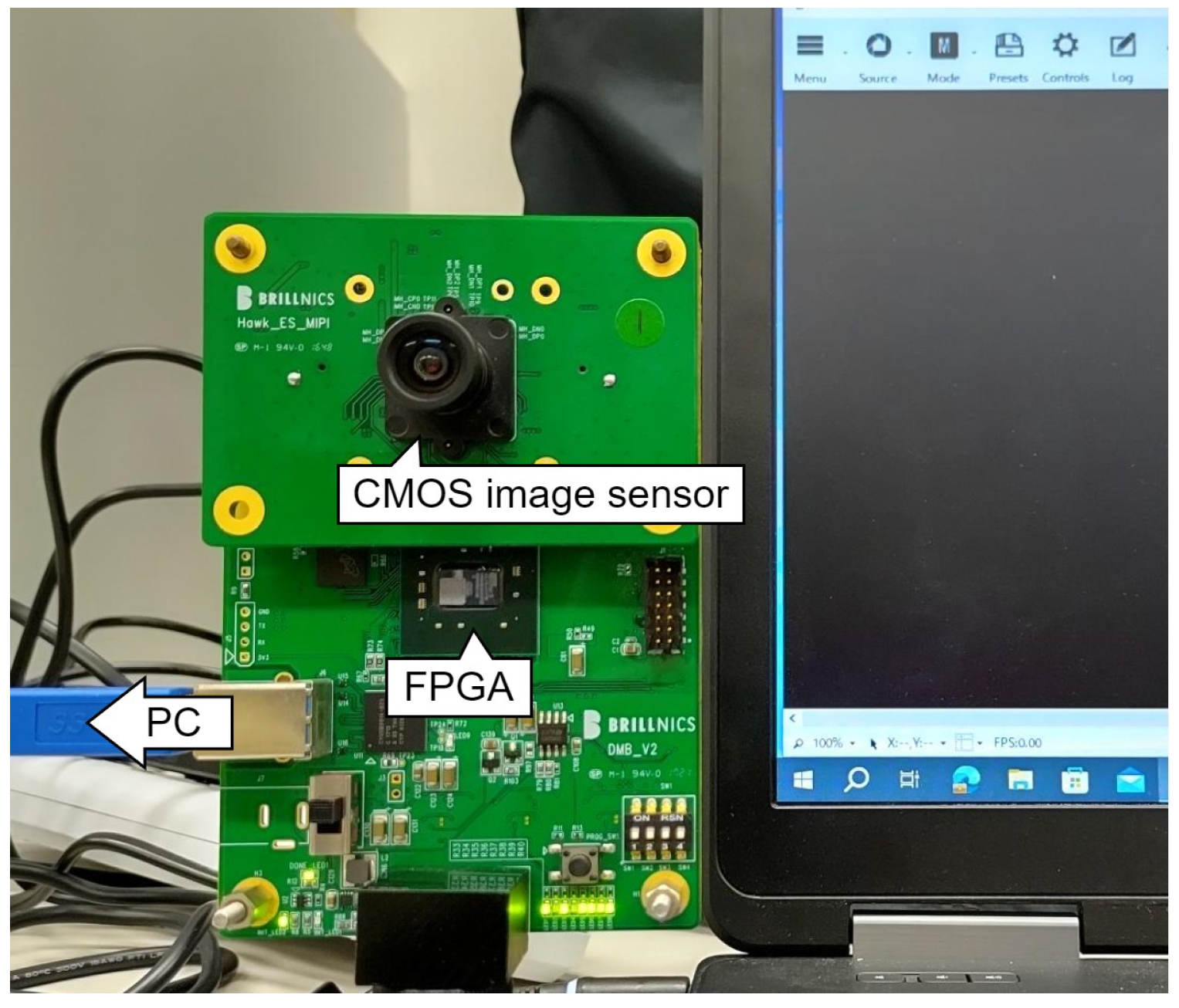
4. Design of the CIS–MAC Circuit

We propose a CMOS image sensor with message authentication in this section. As HMAC does not specify a particular Hash function, we evaluate various Hash functions to select one which is suitable for use in the CIS–MAC. To implement the HMAC in the CMOS image sensor, it is essential to meet two key requirements: (1) High throughput to support high-speed image data readout. (2) a compact circuit area suitable for fabrication using legacy analog processing technology. Based on these requirements, we designed a CIS–MAC circuit with candidate Hash functions and estimated the circuit area using a 0.18 µ m CMOS process.

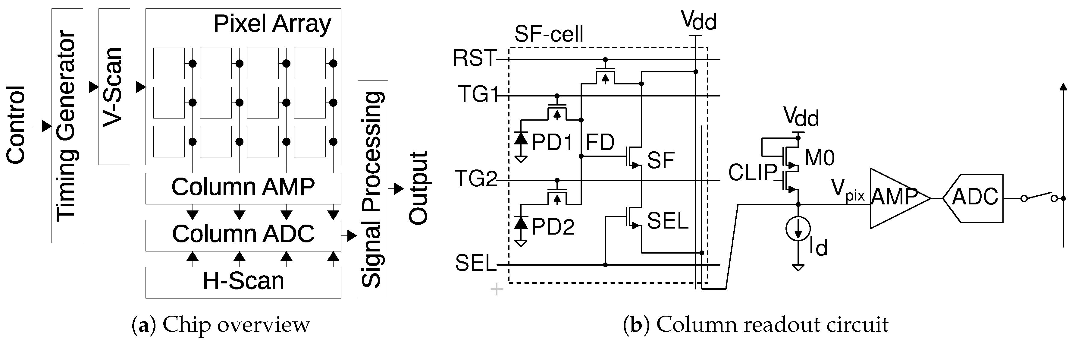
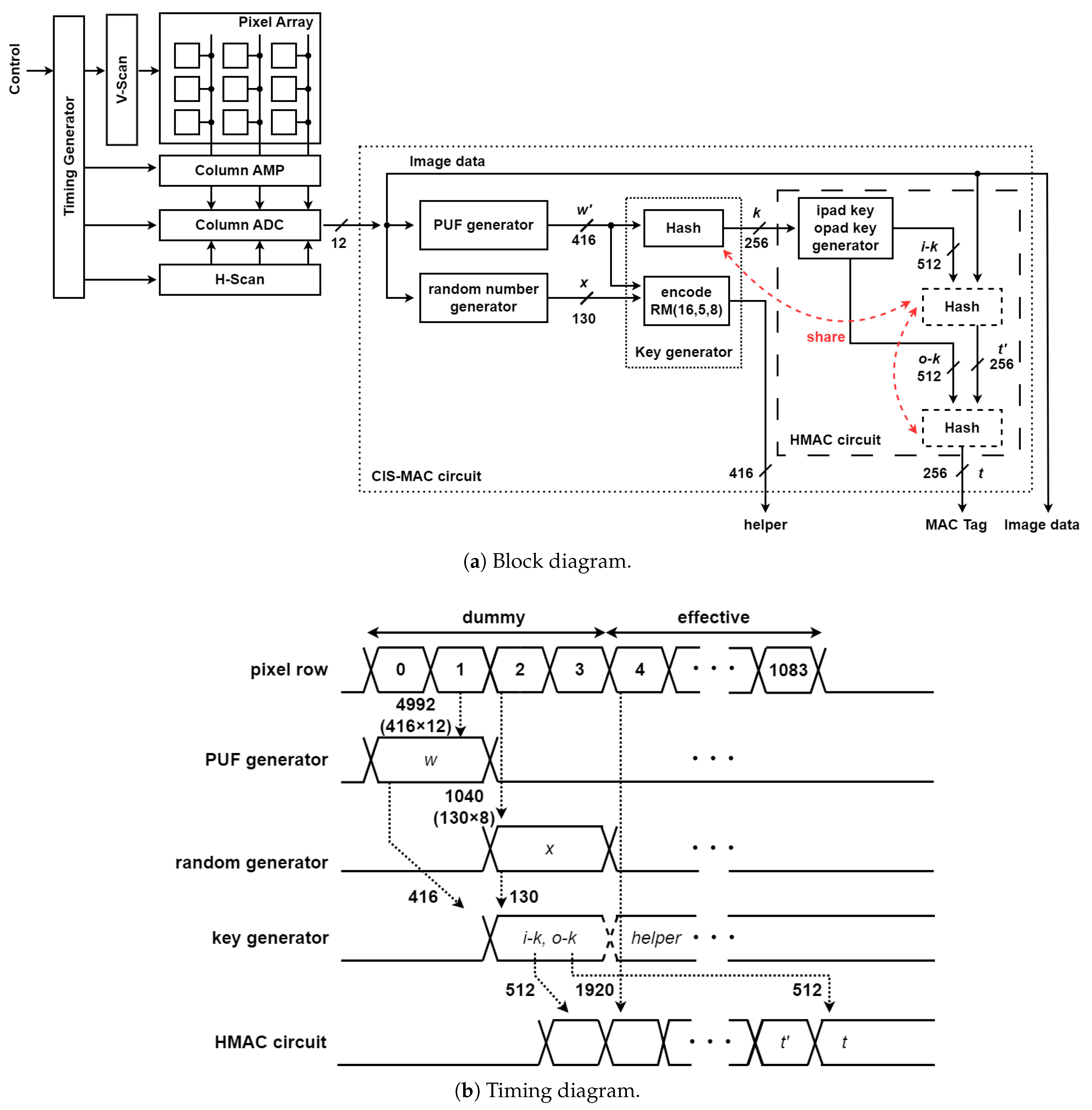
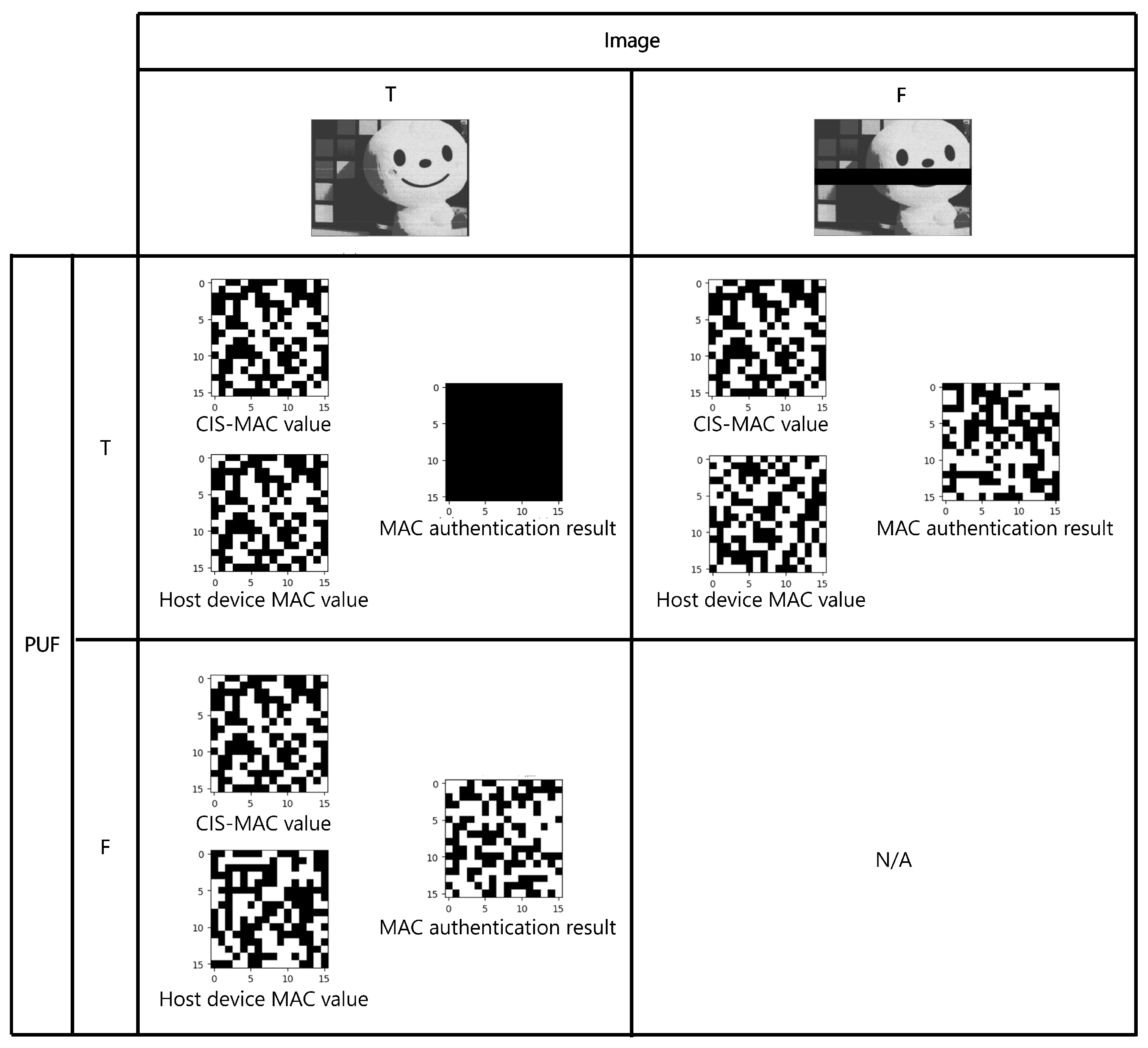
4.1. Proposed CMOS Image Sensor with Message Authentication

We propose a CMOS image sensor with message authentication, the block diagram of which is shown in Figure 9a.
The CIS–MAC circuit sequentially processes the raw PUF data, the raw random numbers, and the image data. The amount of information contained in the helper data generated using the Reed–Muller code RM (16,5) is 5 bits out of 16 bits. Therefore, it is necessary to have 130 bits ( = 26 × 5 bits > 128 bits) of information by using 26 codewords of RM (16,5), considering that an attacker has more than 128 bits of information, to prevent brute force attacks on eavesdropping helper data. At this time, the actual bit length of PUF response w is 416 bits ( = 26 × 16 bits). The PUF generator compares the raw PUF data from vertically adjacent pixels to generate a PUF response with improved uniqueness. The raw PUF data—a 12-bit digitized pixel output in PUF mode—are stored in the PUF generation circuit. After scanning one row of pixels, 416 × 12 bits of raw PUF data are stored. The random number generator applies XOR × 3 operations to multiple raw random data to produce a random number with enhanced randomness and unpredictability. The raw random data, which are 12-bit digitized pixels output in random number mode, are used as input to the random number generator. A 130-bit random number x is generated from 1040 pixels ( 130 × 2 3 ) of raw random data. The helper data are derived from both the PUF response and the random number. The 130-bit random number x is encoded into a 416-bit code c using the RM(16,5,8), where it can be noted that c is shown in Figure 7. The 416-bit helper data h are then generated by applying XOR between the 416-bit PUF response w and the 416-bit code c in the encoding block. As the effective data volume in the 416-bit helper data is 130 bits due to encoding, the success rate of a brute force attack is 2 130 , which is sufficiently low for IoT applications. Meanwhile, the PUF response alone is utilized to generate the cryptographic key through a Hash function. The cryptographic key has a length of 256 bits, meeting the standard for typical 256-bit Hash functions. The 256-bit MAC tag is then generated using the cryptographic key and the image data. As the image data are read out at very high speed, the Hash circuit must support high throughput. To minimize the circuit area, three Hash circuits are shared, and the Hashing operations for the cryptographic key k, the intermediate Hash tag t , and the final Hash tag t are processed sequentially. As a result, the CMOS image sensor outputs the helper data, the MAC tag, and the image data.
The timing diagram of the proposed CMOS image sensor with message authentication is shown in Figure 9b. The raw PUF data and raw random data are read out from the dummy pixel rows, followed by the 1080 effective pixel rows. The cryptographic keys, i-k and o-k, are generated first, following which the PUF response w is cleared at row 2. The key i-k, the 1080 rows of image data, and o-k are subsequently input into the HMAC circuit to generate the MAC tag t.

4.2. Evaluation of Hash Functions for the CIS–MAC

Hash functions that are standardized and can be implemented in IoT devices (e.g., standard Hashes, lightweight Hashes, and next-generation Hashes) [34,35] were evaluated for implementation in CIS–MAC circuits. As Hashing of the image data and the ipad key must match the readout speed of the image data, multiple Hash circuits are time-interleaved based on the input size and processing cycle of the Hash circuit. Suppose that the input size is 32 bits and the processing cycle is 4 clock cycles (4-clk). Given that image data are typically packed in 16-bit words, two Hash circuits are required, as shown in Figure 10.
The number of interleaved Hash circuits, estimated according to the size of the image input data and number of processing cycles, is detailed in Table 4. The area for the entire interleaved Hash circuit could then be estimated from the unit circuit area and the number of interleaved circuits. Notably, SHA2 is a widely utilized standard Hash function [36,37,38]. The evaluated lightweight Hashes included PHOTON [39], QUARK [40], and SPONGENT [41], while the evaluated next-generation Hashes were SHA3 [42] and BLAKE2 [43,44].
Five types of PHOTON Hashes [39] were considered: PHOTON–80/20/16, PHOTON–128/16/16, PHOTON–160/36/36, PHOTON–224/32/32, and PHOTON–256/32/32. The numbers at the end of the name represent the Hash value bit length, input bit rate, and output bit rate, respectively. To support the image input data rate, 106, 156, 80, 102, and 78 interleaved circuits were found to be required, corresponding to interleaved circuit areas of 123.8 , 266.5 , 169.5 , 284.2 , and 340.2 kGE, respectively. QUARK Hashes [40] include three types: U–QUARK, D–QUARK, and S–QUARK. To support the image input data rate, 136, 88, and 32 interleaved circuits were found to be required, resulting in interleaved circuit areas of 325.3 , 248.1 , and 148.5 kGE, respectively. SPONGENT Hashes [41] are available in five types: SPONGENT–88, SPONGENT–128, SPONGENT–160, SPONGENT–224, and SPONGENT–256. The number at the end of the name corresponds to the Hash value bit length. To support the image input data rate, it was found that 90, 140, 90, 120, and 140 interleaved circuits are required, resulting in interleaved circuit areas of 101.4 , 236.2 , 197.1 , 348.4 , and 459.4 kGE, respectively. Although lightweight Hash functions such as PHOTON, QUARK, and SPONGENT have relatively small individual circuit areas, their processing cycles are long relative to the input bit length. As a result, a significant number of interleaved circuits is required, leading to a substantial increase in the total interleaved circuit area.
SHA–3 [42] includes four variants: SHA3–224, SHA3–256, SHA3–384, and SHA3–512, with input bit lengths of 1152 bits, 1088 bits, 832 bits, and 576 bits, respectively. As the processing cycles of these SHA–3 variants enable them to support the image input data rate with a single circuit, the corresponding circuit areas are 31.3 , 31.6 , 31.4 , and 30.7 kGE, respectively. BLAKE2 [43,44] consists of two types: BLAKE2s and BLAKE2b, with input bit lengths of 1024 bits and 512 bits, respectively. The processing times of these BLAKE2 variants are also sufficient to support the image input data rate with a single circuit, with circuit areas of 41.5 and 20.8 kGE, respectively. From the above analysis, while SHA–3 and BLAKE2 have relatively large individual circuit areas, their processing cycles are short relative to the input bit length. As a result, SHA3–512 and BLAKE2s were selected to design CIS–MAC circuits using a 0.18 µ m CMOS process, allowing for estimation of the feasibility of the CIS–MAC circuit with minimal area.

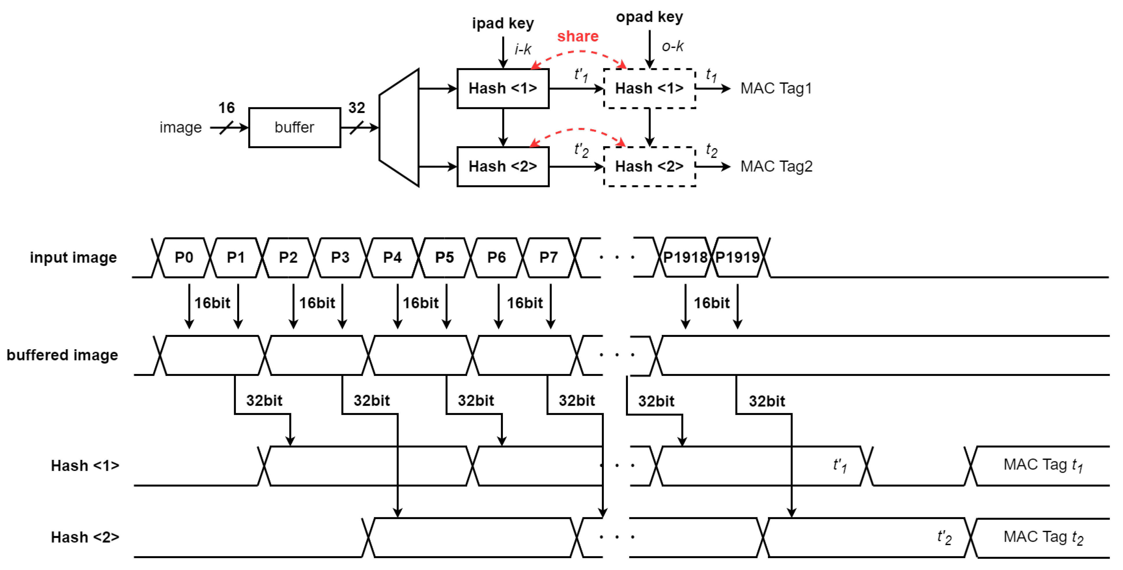
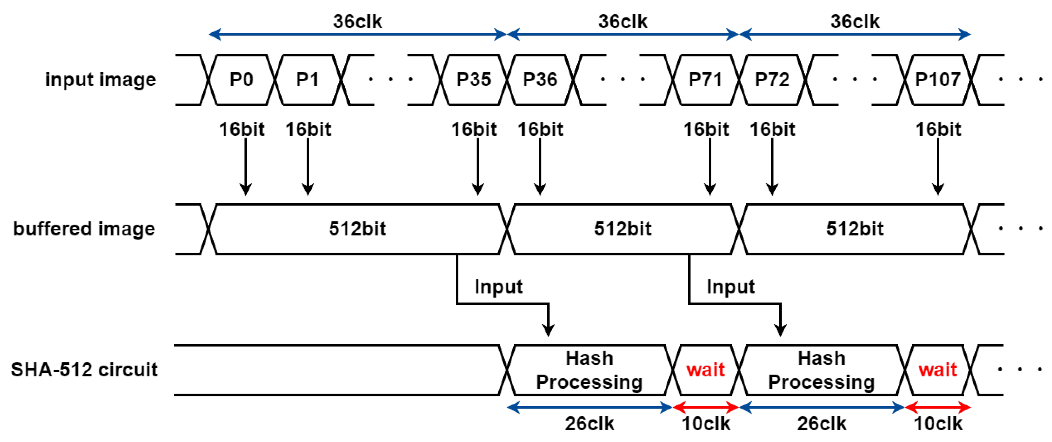
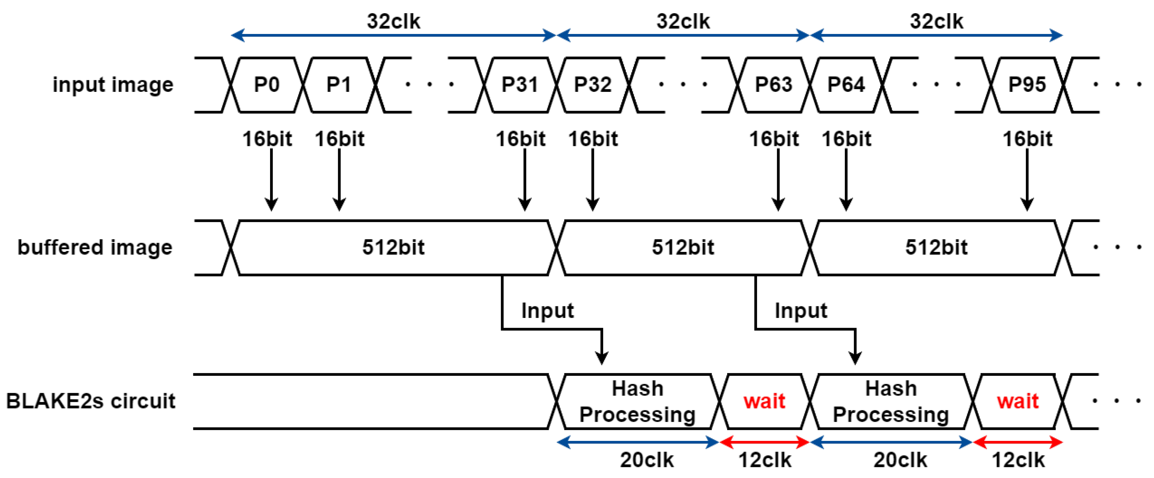
4.3. Timing Design of the HMAC Circuit

Figure 11 shows the operation timing of the HMAC circuit with SHA3–512. Hash processing is performed on each 576-bit block of image data (=16 × 36) as the input block. As the Hash processing requires 26 clock cycles (26-clk), the subsequent input block is processed after a wait of 10 clock cycles (10-clk).
Furthermore, Figure 12 shows the operation timing of the HMAC circuit with BLAKE2s. Hash processing is performed on each 512-bit block of image data (=16 × 32) as the input block. As the Hash processing requires 20 clock cycles (20-clk), the subsequent input block is processed after a wait of 12 clock cycles (12-clk).

4.4. Simulation Results

The CIS–MAC circuits were designed and simulated using Verilog HDL, utilizing measured pixel data. The pixel data consisted of two lines of raw PUF data, two lines of raw random data, and one line of raw image data. The simulation results for the CIS–MAC circuits using SHA3–512 and BLAKE2s are shown in Figure 13 and Figure 14, respectively.
The Hash circuit generates a cryptographic key from the raw PUF data in rows 0 and 1. A random number is derived from the raw random data in rows 2 and 3, and helper data are generated based on the key and the random number. Next, the ‘ipadkey’ and ‘opadkey’ are generated using the derived key. In row 4, the Hash circuit sequentially processes each pixel using the ‘ipadkey’ and the image data as inputs. Once the image data input is complete, the final MAC tag is computed using the ‘opadkey’ and the Hash value output from row 4 as inputs. The image data in row 4 are output without delay, but the final MAC tag costs 1 line of overhead. The Verilog simulation confirmed that the generated key matched that generated using Python (version 3.11.6, Available online: https://www.python.org/downloads/release/python-3116/ (accessed on 31 December 2024)). Similarly, the MAC tag obtained from the Verilog simulation matched that generated with Python.

4.5. Circuit Area Estimation via Logic Synthesis

Logic synthesis was performed on the CIS–MAC circuit using a 0.18 µ m CMOS process [45], in order to estimate the circuit area. The result of logic synthesis, in which the circuit area is given by the equivalent number of NAND gates, is shown in Table 5.
The result for the CIS–MAC circuit using SHA–256 is also shown for comparison. The peripheral area (i.e., other than the Hash circuit), including the PUF response generation circuit. is about 46 kGE. Notably, the peripheral area of the CIS–MAC circuit using SHA–256 circuit was also larger, as control circuits for sequential processing via interleaved Hash circuits needed to be added. As the CIS–MAC circuit using SHA3–512 can generate a MAC using one Hash circuit, the circuit area can be reduced by 37% based on the CIS–MAC circuit using SHA–256. The CIS–MAC circuit using BLAKE2s can reduce the circuit area by 41%. In particular, the area of BLAKE2s—which has a small circuit area—becomes 0.86 mm 2 , and it is possible to mount a circuit capable of MAC authentication with 3.6 % of the circuit area of 3.0 µ m pitch and 1920 × 1080 pixels.

5. Conclusions and Future Work

The MAC value is calculated in real time using the same CIS-PUF as the image captured by the imaging device, and the captured image and MAC are output simultaneously. Generally, the memory implemented in a CIS chip is about one line of pixels, and implementing a large amount of memory in one frame leads to an extreme increase in the chip area, which is unrealistic. Therefore, we proposed a method to calculate the MAC value without storing all the image data in the CIS by sequentially inputting pixel data of the number of bits into the input block of the Hash function. This method will be compatible with any CMOS image sensor by modifying the pixel control sequence and adding CIS-MAC logic circuits, which include a standard hash circuit. Since the CIS-MAC processing occurs based on the pixel readout clock, the proposed CIS-MAC can be applied to higher resolution and/or higher frame rates.
Figure 15 shows the result of MAC authentication to confirm the integrity of the image data and the authenticity of the device. This figures show the output image from the pixel data, the CIS–MAC value generated on the FPGA of the experimental board, the key regenerated on the host device, the MAC values of the host device generated from the received pixel data, and the authentication result of the MAC value, respectively. We verified the case in which the image was tampered with by an attack and the case in which the sensor was spoofed (PUF is different). If the captured image is tampered with before the host device receives it, the MAC values of the host device is changed. To simulate this case, the pixel data values of 100 lines in the captured image are set to 0 before the MAC values of the host device are generated. This changes part of the output captured image to black. In the PUF response, even if the initial value stored in the host device and the value generated by the CIS are different, a reverse fuzzy extractor can correct the error and the generated MAC value is the same. It is also confirmed that the attack is detected when the image data are tampered with or the sensor is manipulated by the different MAC value. These experimental results confirm that the data integrity and device authenticity verification system using the CIS–MAC circuit works correctly as expected.
To complete our approach, we will implement the proposed CIS-MAC in a CMOS image sensor to evaluate the area and power consumption within a constrained floor plan and verify the robustness of the proposed scheme under severe environmental conditions in future work.

6. Summary

First, the security risks associated with image sensor data were described; in particular, adversarial examples (AEs) targeting the MIPI can induce misclassification, making the verification of image data integrity essential. A CMOS image sensor with a message authentication code (CIS–MAC) was proposed as a defense mechanism starting from the image sensor, in order to protect image data from malicious manipulations such as AE attacks. Evaluation results of the physically unclonable function (PUF) response and random number, which are utilized for generation of the cryptographic key and MAC tag, were presented for a 2 Mpixel CMOS image sensor. The minimum entropy of the random number with XOR ×3 was very high ( 0.932590 ), and the random number tests defined in the NIST SP 800–22 were successfully passed in the majority of cases. Furthermore, the PUF response demonstrated high repeatability and uniqueness, and the key recovery error with the Reed–Muller code RM(16,5,8) was less than 0.077 %. According to evaluation of various Hash topologies, SHA3–512 and BLAKE2s were selected as Hash functions that are suitable for key generation and MAC tag generation within the CMOS image sensor. The area of the CIS–MAC circuit was estimated based on a Verilog HDL design and synthesis using a 0.18 µ m CMOS process. The estimated area of the CIS–MAC circuit with BLAKE2 was 67 kGE and 0.86 mm 2 , demonstrating its feasibility for implementation in a typical CMOS image sensor fabricated using analog process technology.

Author Contributions

Conceptualization, H.O., K.Y., T.F. and S.O.; Data curation, Y.R. and M.H.; Formal analysis, Y.R. and T.O.; Funding acquisition, S.O.; Investigation, T.O., H.O. and K.Y.; Methodology, Y.R., M.H., T.O., H.O., K.Y., T.F. and S.O.; Project administration, S.O.; Software, Y.R., M.H. and T.O.; Supervision, T.F. and S.O.; Validation, Y.R., M.H. and T.O.; Writing—original draft, Y.R.; Writing—review and editing, S.O. All authors have read and agreed to the published version of the manuscript.

Funding

This work was supported by JSPS KAKENHI Grant Number JP24K15001.

Data Availability Statement

Data are contained within the article.

Acknowledgments

This work was supported by JSPS KAKENHI Grant Number JP24K15001. This research was conducted in cooperation with Synopsys Corporation through the VLSI Design and Education Center, the University of Tokyo. The library used in this research is the result of Tamaru/Onodera Laboratory, Graduate School of Informatics, Kyoto University, and was released by Kazutoshi Kobayashi, Kyoto Institute of Technology. I would like to express my deep gratitude to all involved.

Conflicts of Interest

The authors declare no conflict of interest.

References

  1. Li, J.; Seok, M. A 3.07 μm2/bitcell physically unclonable function with 3.5% and 1% bit-instability across 0 to 80 ∘C and 0.6 to 1.2 V in a 65 nm CMOS. In Proceedings of the Symposia on VLSI Technology and Circuits, Kyoto, Japan, 16–19 June 2015; pp. C250–C251. [Google Scholar] [CrossRef]
  2. Yoshimoto, Y.; Katoh, Y.; Ogasahara, S.; Wei, Z.; Kouno, K. A ReRAM-based physically unclonable function with bit error rate <0.5% after 10 years at 125 ∘C for 40 nm embedded application. In Proceedings of the Symposia on VLSI Technology and Circuits, Honolulu, HI, USA, 13–17 June 2016; pp. 1–2. [Google Scholar] [CrossRef]
  3. Willers, O.; Huth, C.; Guajardo, J.; Seidel, H. MEMS-Based Gyroscopes as Physical Unclonable Functions; IEICE Technical Committee on CCS Computer and Communications Security: Vienna, Austria, 24–28 October 2016. [Google Scholar]
  4. Chen, J.; Tanamoto, T.; Noguchi, H.; Mitani, Y. Further investigations on traps stabilities in random telegraph signal noise and the application to a novel concept physical unclonable function (PUF) with robust reliabilities. In Proceedings of the Symposia on VLSI Technology and Circuits, Kyoto, Japan, 16–19 June 2015; pp. T40–T41. [Google Scholar] [CrossRef]
  5. Cao, Y.; Zhang, L.; Zalivaka, S.S.; Chang, C.H.; Chen, S. CMOS Image Sensor Based Physical Unclonable Function for Coherent Sensor-Level Authentication. IEEE TCAS-I 2015, 62, 2629–2640. [Google Scholar] [CrossRef]
  6. Lu, L.; Kim, T.T.H. A High Reliable SRAM-Based PUF With Enhanced Challenge-Response Space. IEEE Trans. Circuits Syst. II Express Briefs 2022, 69, 589–593. [Google Scholar] [CrossRef]
  7. Lin, B.; Pang, Y.; Gao, B.; Tang, J.; Wu, D.; Chang, T.W.; Lin, W.E.; Sun, X.; Yu, S.; Chang, M.F.; et al. A Highly Reliable RRAM Physically Unclonable Function Utilizing Post-Process Randomness Source. IEEE J. Solid-State Circuits 2021, 56, 1641–1650. [Google Scholar] [CrossRef]
  8. Okura, S.; Nakura, Y.; Shirahata, M.; Shiozaki, M.; Kubota, T.; Ishikawa, K.; Takayanagi, I.; Fujino, T. A Proposal of PUF Utilizing Pixel Variations in the CMOS Image Sensor. In Proceedings of the International Image Sensor Workshop, Hiroshima, Japan, 30 May–2 June 2017; pp. 66–69. [Google Scholar]
  9. Okura, S.; Ishiki, R.; Shirahata, M.; Kubota, T.; Shiozaki, M.; Ishikawa, K.; Takayanagi, I.; Fujino, T. A Dynamic Soft-Decision Fuzzy Extractor for a CMOS Image Sensor PUF. In Proceedings of the 2018 ISPACS, Ishigaki, Japan, 27–30 November 2018. [Google Scholar]
  10. Turay, T.; Vladimirova, T. Toward Performing Image Classification and Object Detection with Convolutional Neural Networks in Autonomous Driving Systems: A Survey. IEEE Access 2022, 10, 14076–14119. [Google Scholar] [CrossRef]
  11. Fujiyoshi, H.; Hirakawa, T.; Yamashita, T. Deep learning-based image recognition for autonomous driving. IATSS Res. 2019, 43, 244–252. [Google Scholar] [CrossRef]
  12. Badjie, B.; Cecílio, J.; Casimiro, A. Adversarial Attacks and Countermeasures on Image Classification-based Deep Learning Models in Autonomous Driving Systems: A Systematic Review. ACM Comput. Surv. 2024, 57, 1–52. [Google Scholar] [CrossRef]
  13. Suman, S.; Kumar, D.; Kumar, A. Fuzzy Based Convolutional Noise Clustering Classifier to Handle the Noise and Heterogeneity in Image Classification. Mathematics 2022, 10, 4056. [Google Scholar] [CrossRef]
  14. Oyama, T.; Okura, S.; Yoshida, K.; Fujino, T. Backdoor attack on deep neural networks triggered by fault injection attack on image sensor interface. In Proceedings of the 5th Workshop on Attacks and Solutions in Hardware Security, Virtual, 19 November 2021; pp. 63–72. [Google Scholar]
  15. Liu, W.; He, W.; Hu, B.; Chang, C.H. A practical man-in-the-middle attack on deep learning edge device by sparse light strip injection into camera data lane. In Proceedings of the 2022 IEEE 35th International System-on-Chip Conference (SOCC), Belfast, UK, 5–8 September 2022; pp. 1–6. [Google Scholar]
  16. Jiang, Q.; Ji, X.; Yan, C.; Xie, Z.; Lou, H.; Xu, W. GlitchHiker: Uncovering vulnerabilities of image signal transmission with IEMI. In Proceedings of the 32nd USENIX Security Symposium (USENIX Security 23), Anaheim, CA, USA, 9–11 August 2023; pp. 7249–7266. [Google Scholar]
  17. Szegedy, C.; Zaremba, W.; Sutskever, I.; Bruna, J.; Erhan, D.; Goodfellow, I.; Fergus, R. Intriguing properties of neural networks. arXiv 2013, arXiv:1312.6199. [Google Scholar]
  18. Goodfellow, I.J.; Shlens, J.; Szegedy, C. Explaining and harnessing adversarial examples. arXiv 2014, arXiv:1412.6572. [Google Scholar]
  19. Gu, T.; Dolan-Gavitt, B.; Garg, S. Badnets: Identifying vulnerabilities in the machine learning model supply chain. arXiv 2017, arXiv:1708.06733. [Google Scholar]
  20. Gu, T.; Liu, K.; Dolan-Gavitt, B.; Garg, S. Badnets: Evaluating backdooring attacks on deep neural networks. IEEE Access 2019, 7, 47230–47244. [Google Scholar] [CrossRef]
  21. Oyama, T.; Yoshida, K.; Okura, S.; Fujino, T. Fundamental study of adversarial examples created by fault injection attack on image sensor interface. In Proceedings of the 2022 Asian Hardware Oriented Security and Trust Symposium (AsianHOST), Singapore, 14–16 December 2022; pp. 1–6. [Google Scholar]
  22. Versaci, M.; Angiulli, G.; La Foresta, F.; Laganà, F.; Palumbo, A. Intuitionistic fuzzy divergence for evaluating the mechanical stress state of steel plates subject to bi-axial loads. Integr. Comput.-Aided Eng. 2024, 31, 1–17. [Google Scholar] [CrossRef]
  23. Stallkamp, J.; Schlipsing, M.; Salmen, J.; Igel, C. Man vs. computer: Benchmarking machine learning algorithms for traffic sign recognition. Neural Netw. 2012, 32, 323–332. [Google Scholar] [CrossRef] [PubMed]
  24. Simonyan, K.; Zisserman, A. Very deep convolutional networks for large-scale image recognition. arXiv 2014, arXiv:1409.1556. [Google Scholar]
  25. Maes, R.; Peeters, R.; Herrewege, A.; Wachsmann, C.; Katzenbeisser, S.; Sadeghi, A.R.; Verbauwhede, I. Reverse Fuzzy Extractors: Enabling Lightweight Mutual Authentication for PUF-enabled RFIDs. In Proceedings of the Financial Cryptography and Data Security: 16th International Conference, FC 2012, Kralendijk, Bonaire, 27 Februray–2 March 2012; Revised Selected Papers 16. pp. 374–389. [Google Scholar] [CrossRef]
  26. Dodis, Y.; Reyzin, L.; Smith, A. Fuzzy extractors: How to generate strong keys from biometrics and other noisy data. In Proceedings of the Advances In Cryptology-EUROCRYPT 2004: International Conference On The Theory And Applications Of Cryptographic Techniques, Interlaken, Switzerland, 2–6 May 2004; Proceedings 23. Springer: Berlin/Heidelberg, Germany, 2004; pp. 523–540. [Google Scholar]
  27. Okura, S.; Ishiki, R.; Takano, S.; Shirahata, M.; Kubota, T.; Shiozaki, M.; Ishikawa, K.; Takayanagi, I.; Fujino, T. A 2-Mpixel CMOS Image Sensor with Device Authentication and Encryption Key Generation based on Physically Unclonable Function. In Proceedings of the International Image Sensor Workshop, Snowbird Resort, UT, USA, 24–27 June 2019; pp. 119–122. [Google Scholar]
  28. Shiozaki, M.; Hori, Y.; Fujino, T. Entropy Estimation of Physically Unclonable Functions with Offset Error. Cryptology ePrint Archive, Paper 2020/1284. 2020. Available online: https://eprint.iacr.org/2020/1284 (accessed on 31 December 2024).
  29. Zhang, R.; Wang, X.; Liu, K.; Shinohara, H. A 0.186-pJ per Bit Latch-Based True Random Number Generator Featuring Mismatch Compensation and Random Noise Enhancement. IEEE J. Solid-State Circuits 2022, 57, 2498–2508. [Google Scholar] [CrossRef]
  30. Turan, M.S.; Barker, E.; Kelsey, J.; McKay, K.; Baish, M.; Boyle, M. NIST, SP 800–90B: Recommendation for the Entropy Sources Used for Random Bit Generation; Technical Report; National Institute of Standards and Technology: Gaithersburg, MD, USA, 2018. [Google Scholar]
  31. Clavier, C.; Gaj, K. Cryptographic Hardware and Embedded Systems-CHES 2009: 11th International Workshop Lausanne, Switzerland, 6–9 September 2009; Proceedings; Springer Science & Business Media: Berlin/Heidelberg, Germany, 2009; Volume 5747. [Google Scholar]
  32. Maes, R.; Tuyls, P.; Verbauwhede, I. A soft decision helper data algorithm for SRAM PUFs. In Proceedings of the 2009 IEEE International Symposium on Information Theory, Seoul, Republic of Korea, 28 June–3 July 2009; pp. 2101–2105. [Google Scholar] [CrossRef]
  33. Turner, J.M. The keyed-hash message authentication code (hmac). Fed. Inf. Process. Stand. Publ. 2008, 198, 1–13. [Google Scholar]
  34. Abed, S.; Jaffal, R.; Mohd, B.J.; Al-Shayeji, M. An analysis and evaluation of lightweight hash functions for blockchain-based IoT devices. Clust. Comput. 2021, 24, 3065–3084. [Google Scholar] [CrossRef]
  35. Rao, V.; Prema, K.V. Light-weight hashing method for user authentication in Internet-of-Things. Ad Hoc Netw. 2019, 89, 97–106. [Google Scholar] [CrossRef]
  36. Dobraunig, C.; Eichlseder, M.; Mendel, F. Security Evaluation of sha-224, sha-512/224, and sha-512/256; Institute for Applied Information Processing and Communications, Graz University of Technology: Graz, Austria, 2015. [Google Scholar]
  37. Turan, M.S.; Perlner, R.; Bassham, L.E.; Burr, W.; Chang, D.; jen Chang, S.; Dworkin, M.J.; Kelsey, J.M.; Paul, S.; Peralta, R. Status Report on the Second Round of the SHA-3 Cryptographic Hash Algorithm Competition; NIST Interagency Report; National Institute of Standards and Technology: Gaithersburg, MD, USA, 2011; Volume 7764. [Google Scholar]
  38. Sekioka, Y.; Oyama, T.; Tatsuno, H.; Yoshida, K.; Okura, S.; Fujino, T. A Study on Small Area HMAC-SHA256 Circuit Suitable for CMOS Image Sensor; Technical Report; HWS Technical Committee on Hardware Security; Institute of Electronics, Information and Communication Engineers: Tokyo, Japan, 7–8 March 2022; Volume 122. [Google Scholar]
  39. Guo, J.; Peyrin, T.; Poschmann, A. The PHOTON Family of Lightweight Hash Functions. Cryptology ePrint Archive, Paper 2011/609. 2011. Available online: https://eprint.iacr.org/2011/609.pdf (accessed on 31 December 2024).
  40. Aumasson, J.P.; Henzen, L.; Meier, W.; Naya-Plasencia, M. Quark: A Lightweight Hash. J. Cryptol. 2013, 26, 313–339. [Google Scholar] [CrossRef]
  41. Bogdanov, A.; Knezevic, M.; Leander, G.; Toz, D.; Varici, K.; Verbauwhede, I. SPONGENT: The Design Space of Lightweight Cryptographic Hashing. Cryptology ePrint Archive, Paper 2011/697. 2011. Available online: https://eprint.iacr.org/2011/697.pdf (accessed on 31 December 2024).
  42. Nannipieri, P.; Bertolucci, M.; Baldanzi, L.; Crocetti, L.; Di Matteo, S.; Falaschi, F.; Fanucci, L.; Saponara, S. SHA2 and SHA-3 accelerator design in a 7 nm technology within the European Processor Initiative. Microprocess. Microsystems 2021, 87, 103444. [Google Scholar] [CrossRef]
  43. Aumasson, J.P.; Neves, S.; Wilcox-O’Hearn, Z.; Winnerlein, C. BLAKE2: Simpler, smaller, fast as MD5. Cryptology ePrint Archive, Paper 2013/322. 2013. Available online: https://eprint.iacr.org/2013/322 (accessed on 31 December 2024).
  44. Saarinen, M.J.O.; Aumasson, J.P. The BLAKE2 Cryptographic Hash and Message Authentication Code (MAC); RFC 7693; Internet Engineering Task Force: Fremont, CA, USA, 2015. [Google Scholar] [CrossRef]
  45. Onodera, H.; Hirata, A.; Kitamura, T.; Kobayashi, K.; Tamaru, K. P2Lib: Process Portable Library and Its Generation System. Trans. Inf. Process. Soc. Jpn. 1999, 40, 1660–1669. [Google Scholar]
Figure 1. Attack flow of the adversary.
Electronics 14 01971 g001
Figure 2. The proposed Hash-based message authentication scheme.
Electronics 14 01971 g002
Figure 3. Measurement environment.
Electronics 14 01971 g003
Figure 4. Block diagrams.
Electronics 14 01971 g004
Figure 5. Timing diagrams for different CMOS image sensor operation modes.
Electronics 14 01971 g005
Figure 6. PUF response evaluation results.
Electronics 14 01971 g006
Figure 7. Fuzzy extractor circuit block diagram.
Electronics 14 01971 g007
Figure 8. The overview of HMAC.
Electronics 14 01971 g008
Figure 9. Proposed CMOS image sensor with message authentication.
Electronics 14 01971 g009
Figure 10. Diagram of interleaved Hash processing.
Electronics 14 01971 g010
Figure 11. SHA3–512 image processing timing.
Electronics 14 01971 g011
Figure 12. BLAKE2s image processing timing.
Electronics 14 01971 g012
Figure 13. Simulation result of CIS–MAC circuit using SHA3–512.
Electronics 14 01971 g013
Figure 14. Simulation result of CIS–MAC circuit using BLAKE2s.
Electronics 14 01971 g014
Figure 15. The result of MAC authentication.
Electronics 14 01971 g015
Table 1. Readout signal for each operation mode.
ModeImagingPUFRandom Number
Optical Signalreadoutremovedcanceled
Vth variationcanceledreadout ( 100 mV pp )canceled
kTC noisecanceledreadout ( 10 mV pp )readout
Table 2. The results of the random number test NIST SP 800–90B for the output random number data.
#XORMin. Entropy
XOR ×00.780533
XOR ×10.907243
XOR ×20.923184
XOR ×30.932590
Table 3. Result of the random number test NIST 800–22 for the output random number data.
(A) Ave. p-Value(A) Passed(B) Ave. p-Value(B) Passed
Frequency0.0000000/600.27570959/60
BlockFrequency0.0000000/600.46859559/60
CumulativeSums0.0000000/600.94960259/60
Runs0.0000000/600.93195258/60
LongestRun0.0000000/600.88813759/60
Rank0.43727459/600.93195258/60
FFT0.0000000/600.29925157/60
NonOverlappingTemplate0.00029655/600.97606060/60
OverlappingTemplate0.0000000/600.80433759/60
Universal0.0000000/600.67177959/60
ApproximateEntropy0.0000000/600.56805558/60
RandomExcursions0.80433738/38
RandomExcursionsVariant0.73991837/38
Serial0.0000008/600.56805559/60
LinearComplexity0.83430859/600.96429560/60
Table 4. Comparison of circuit area when applying various Hash functions in CIS–MAC circuit.
Hash CircuitInput Bits [bit]Cycle [clk]Number of Interleaved CircuitsCircuit Area [kGE/Unit]Area of the Entire Interleaved Circuit [kGE]
SHA–2565126831339
SHA–512102488228.456.8
PHOTON 80/20/16201321061.2123.8
PHOTON 128/16/16161561561.7266.5
PHOTON 160/36/3636180802.1169.4
PHOTON 224/32/32322041022.8284.2
PHOTON 256/32/3232156784.4340.2
U–Quark8681362.4325.3
D–Quark1688882.8248.1
S–Quark3264324.6148.5
SPONGENT–88845901.1101.4
SPONGENT–1288701401.7236.2
SPONGENT–1601690902.2197.1
SPONGENT–224161201202.9348.4
SPONGENT–256161401403.3459.3
SHA3–224115225131.331.3
SHA3–256108825131.631.6
SHA3–38483225131.431.4
SHA3–51257625130.730.7
BLAKE2b102429141.541.5
BLAKE2s51220120.820.8
Table 5. CIS–MAC logic synthesis results.
Hash CircuitCircuit Area [GE]
SHA–256113k (Hash circuit: 13k)
SHA3–51271k (Hash circuit: 26k)
BLAKE2s67k (Hash circuit: 21k)
Disclaimer/Publisher’s Note: The statements, opinions and data contained in all publications are solely those of the individual author(s) and contributor(s) and not of MDPI and/or the editor(s). MDPI and/or the editor(s) disclaim responsibility for any injury to people or property resulting from any ideas, methods, instructions or products referred to in the content.

