
FATE: A Flexible FPGA-Based Automatic Test Equipment for Digital ICs


Abstract
1. Introduction
- In this study, we designed a configurable test channel, which can achieve different chip test items, to detect the chip’s functional faults, delay faults, etc., and provide more test channels to adapt to more chips.
- In the case of a limited number of interfaces, the system supports test vectors of any length by round-robin scheduling interface transmissions, thereby improving fault coverage.
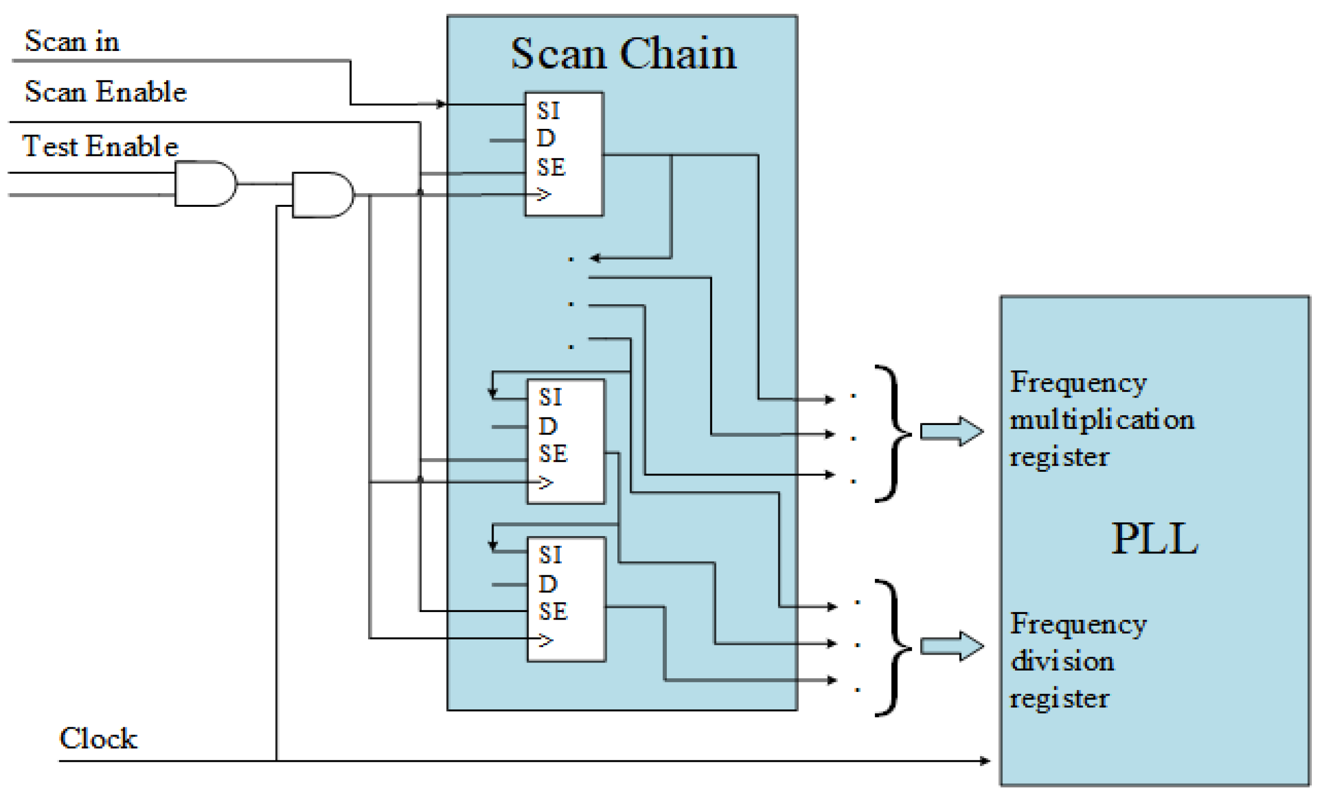
- Based on the structure of the chip’s design for testability, the frequency scanning test method can quickly obtain the limit performance of the chip for the appropriate scene.
2. DFT and Related Works
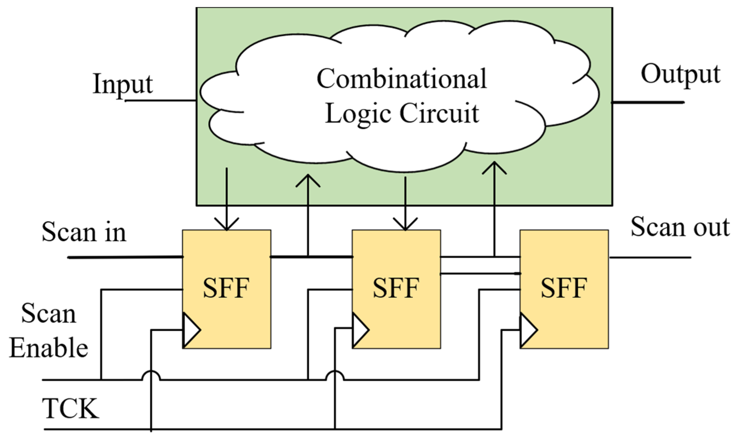
2.1. Scan Test Design
2.2. Related Works
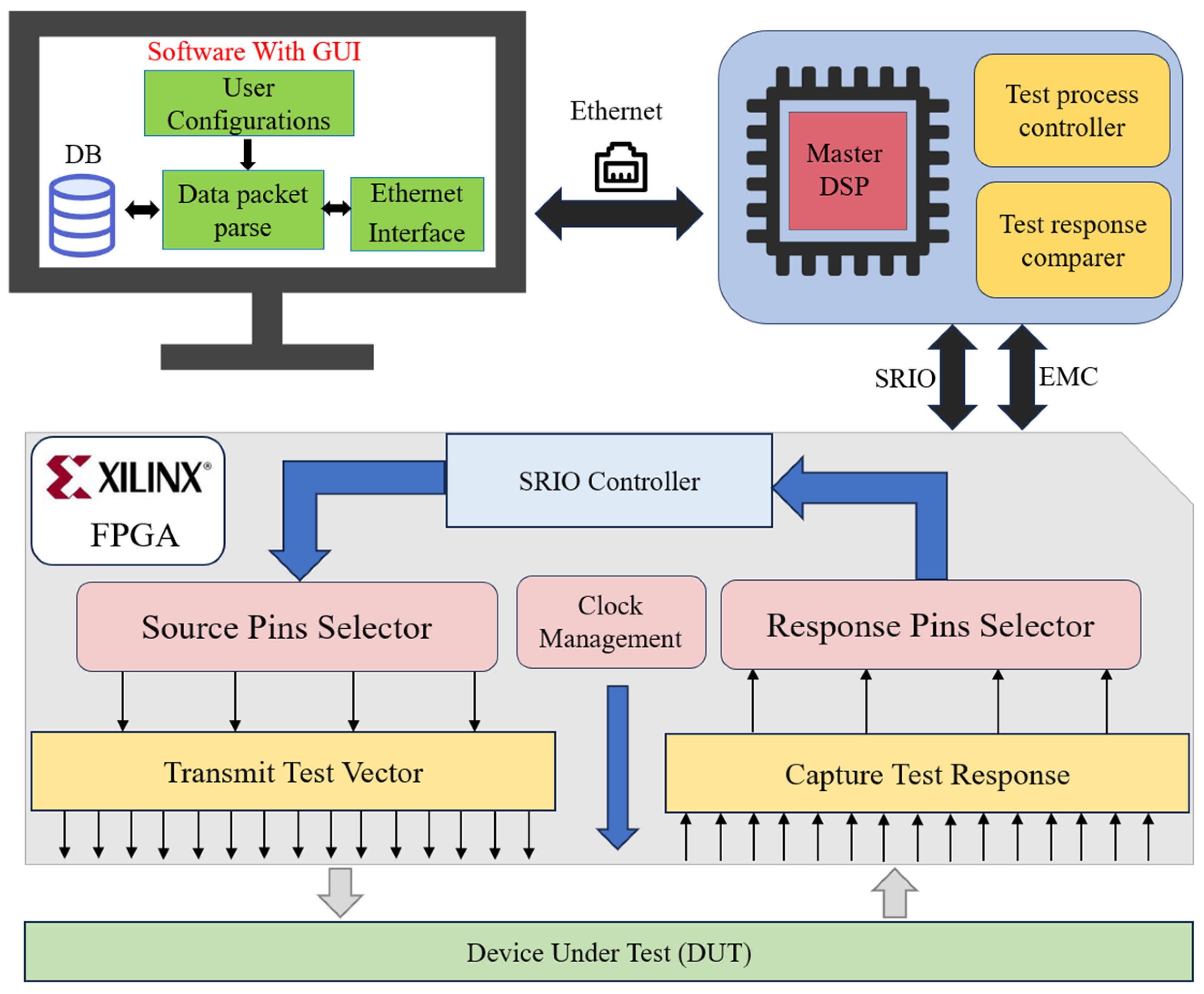
3. FATE System Design
3.1. Overview
3.2. Hardware Design of FATE
3.2.1. Test Channel
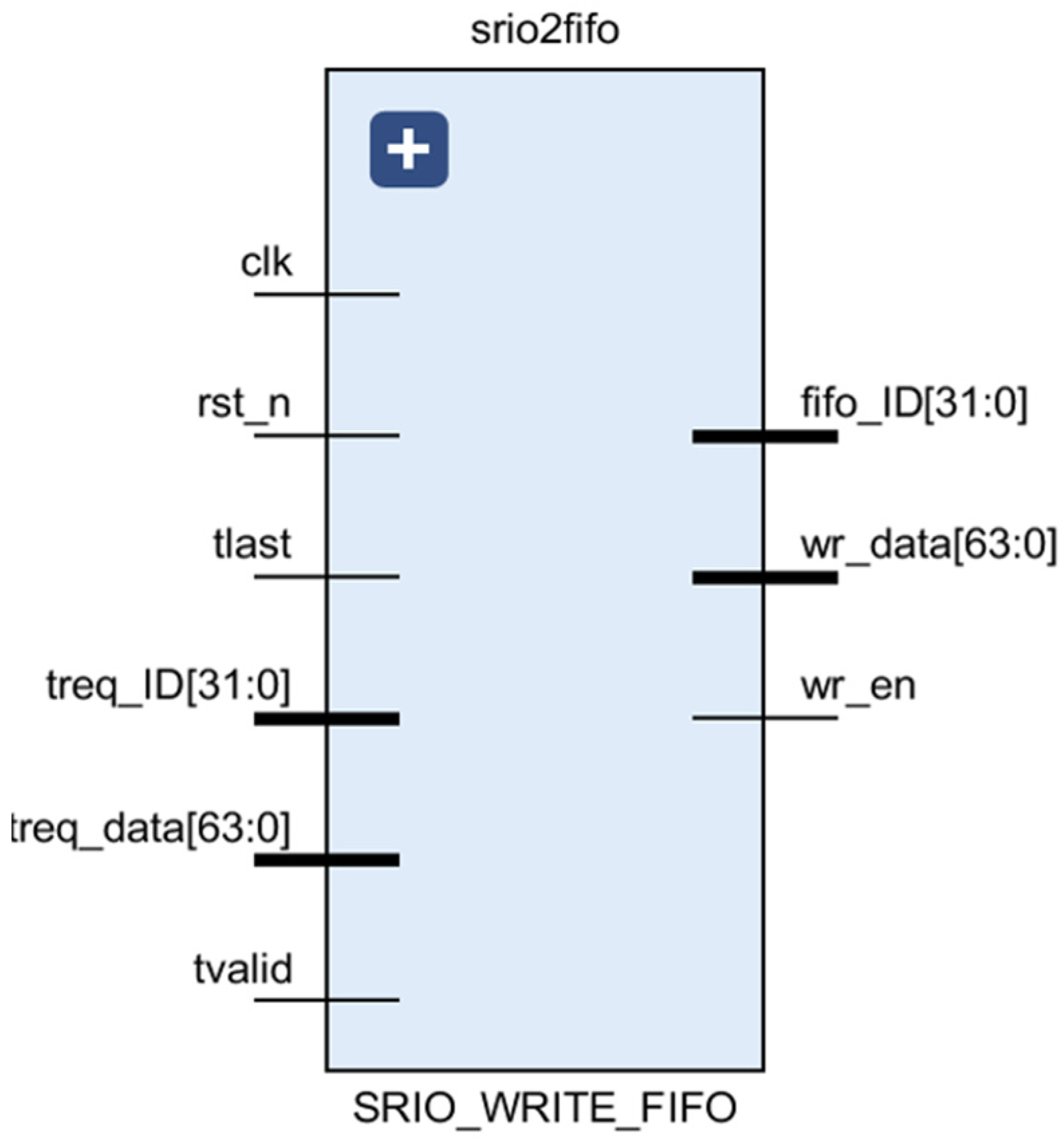
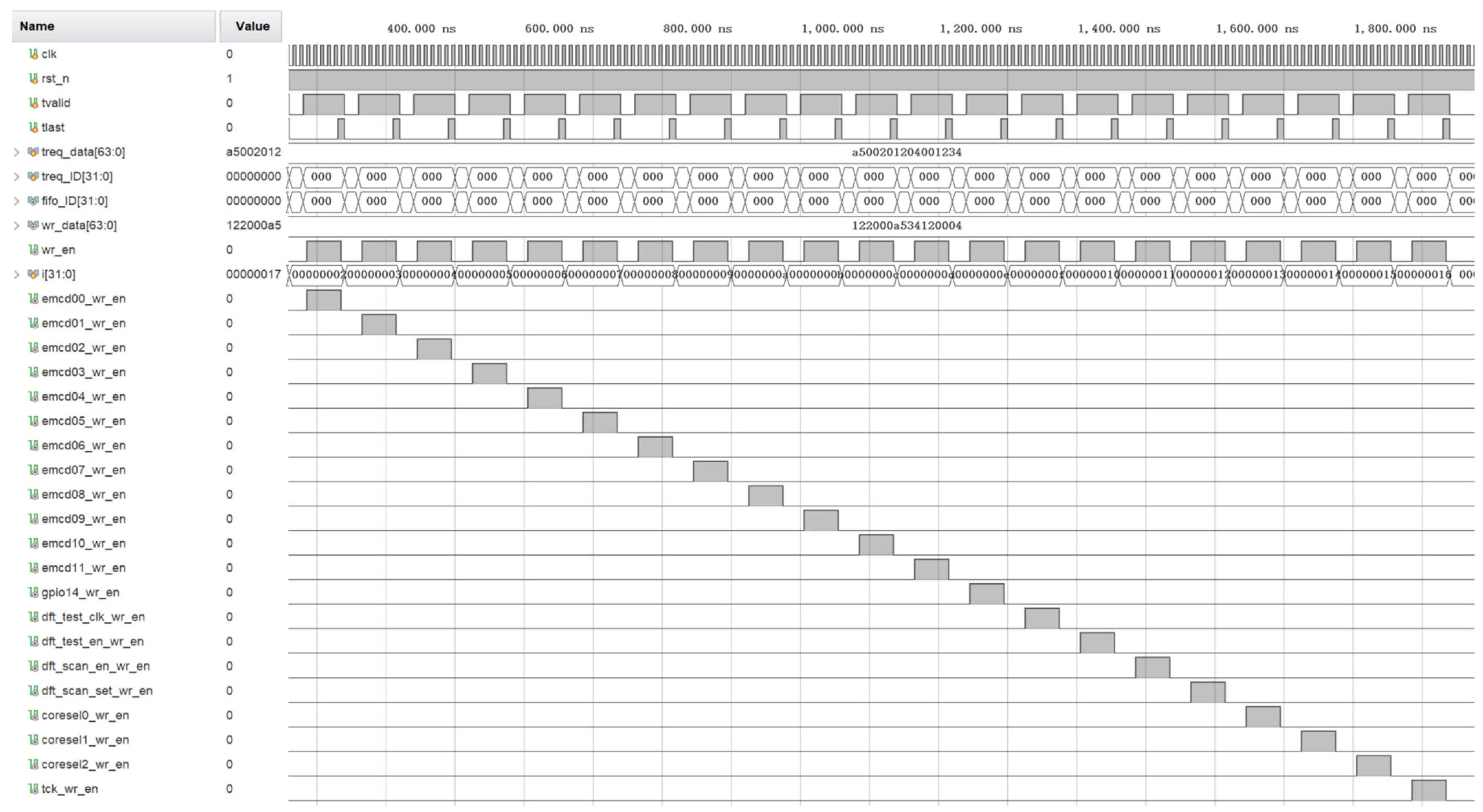
3.2.2. SRIO Controller
3.2.3. Configurable Design of Test Channels
3.2.4. Clock Management Module
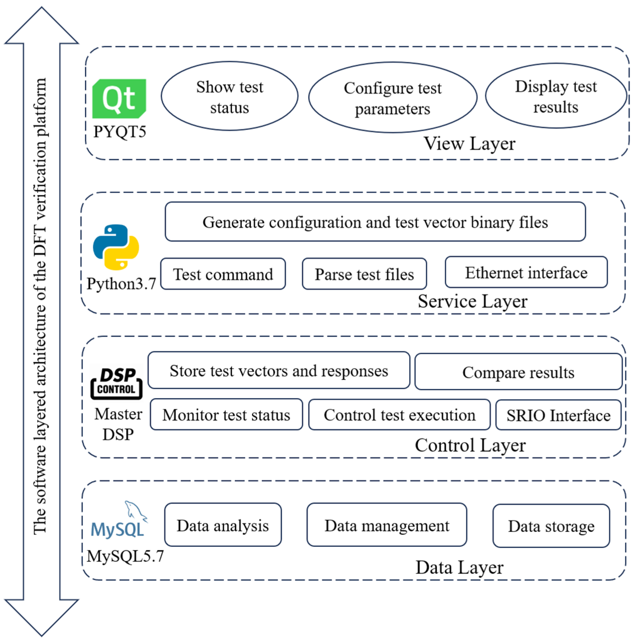
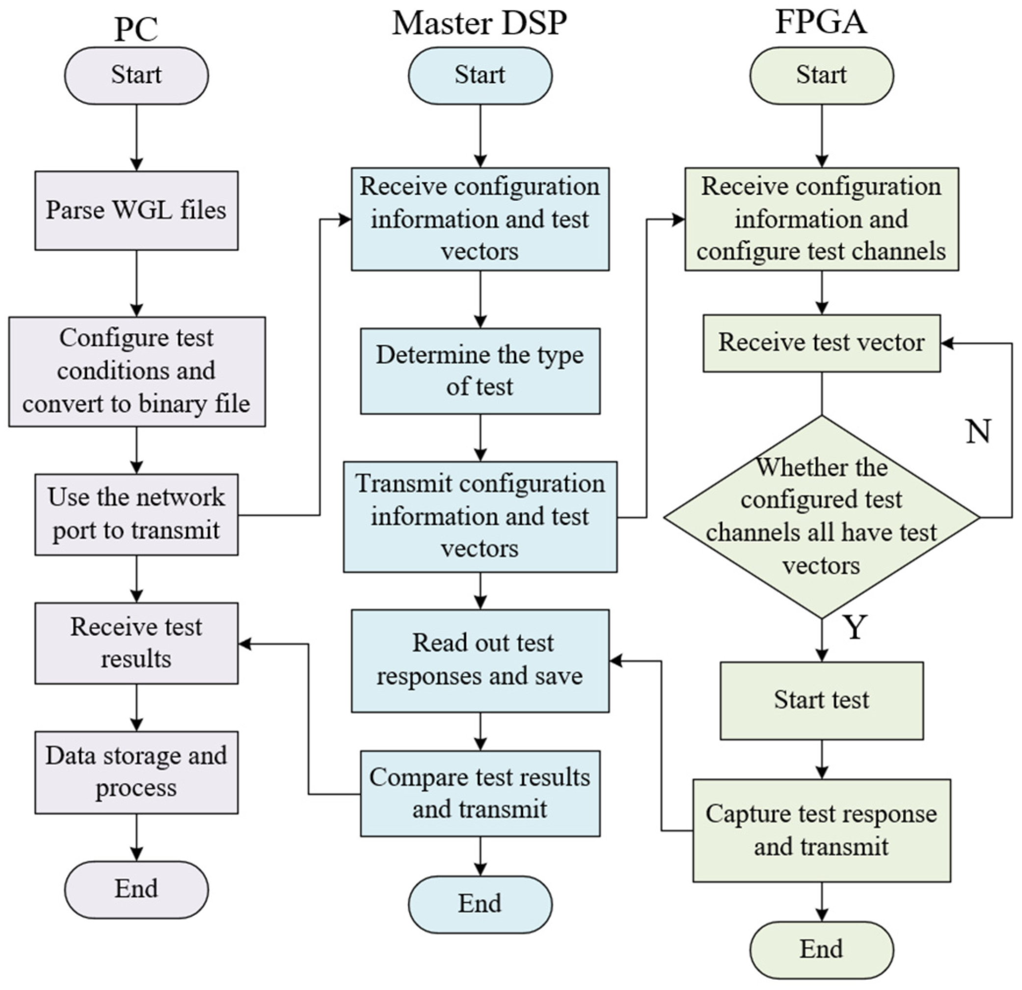
3.3. Software Design of FATE
3.3.1. Overall Software Design
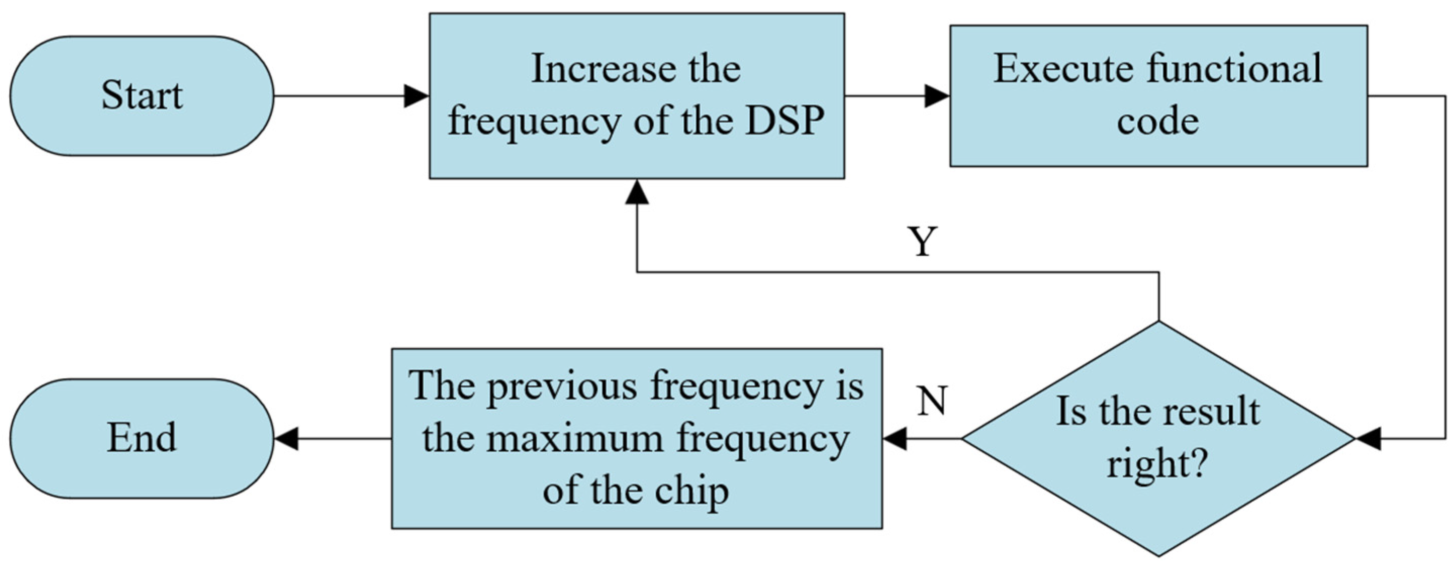
3.3.2. Chip Performance Test
3.3.3. Round-Robin Scheduling Transmit
| Algorithm 1. Round-robin scheduling algorithm |
| Input: Number of input pins X, Number of output pins Y, Threshold value Q, Depth of the FIFO H, Length of the test vector L, Length of completed transmission of test vectors P, Threshold flags T Initial: P = 0 1: for (i = 1 to X) do 2: Master DSP transmits a test vector of length H to input channel i. 3: end for |
| 4: P = P + H |
| 5: while (L − P > Q) do 6: if T then |
| 7: for (i = 1 to Y) do 8: FPGA transmits the test response of length Q from the output channel i to the Master DSP. 9: end for 10: for (i = 1 to X) do 11: Master DSP transmits a test vector of length Q to input channel i. 12: end for |
| 13: P = P + Q |
| 14: end if 15: for (i = 1 to X) do |
| 16: Master DSP transmits a test vector of length (L − P) to the input channel i. 17: end for 18: for (i = 1 to Y) do |
| 19: FPGA transmits the remaining test responses from the output channel i to the Master DSP. 20: end for |
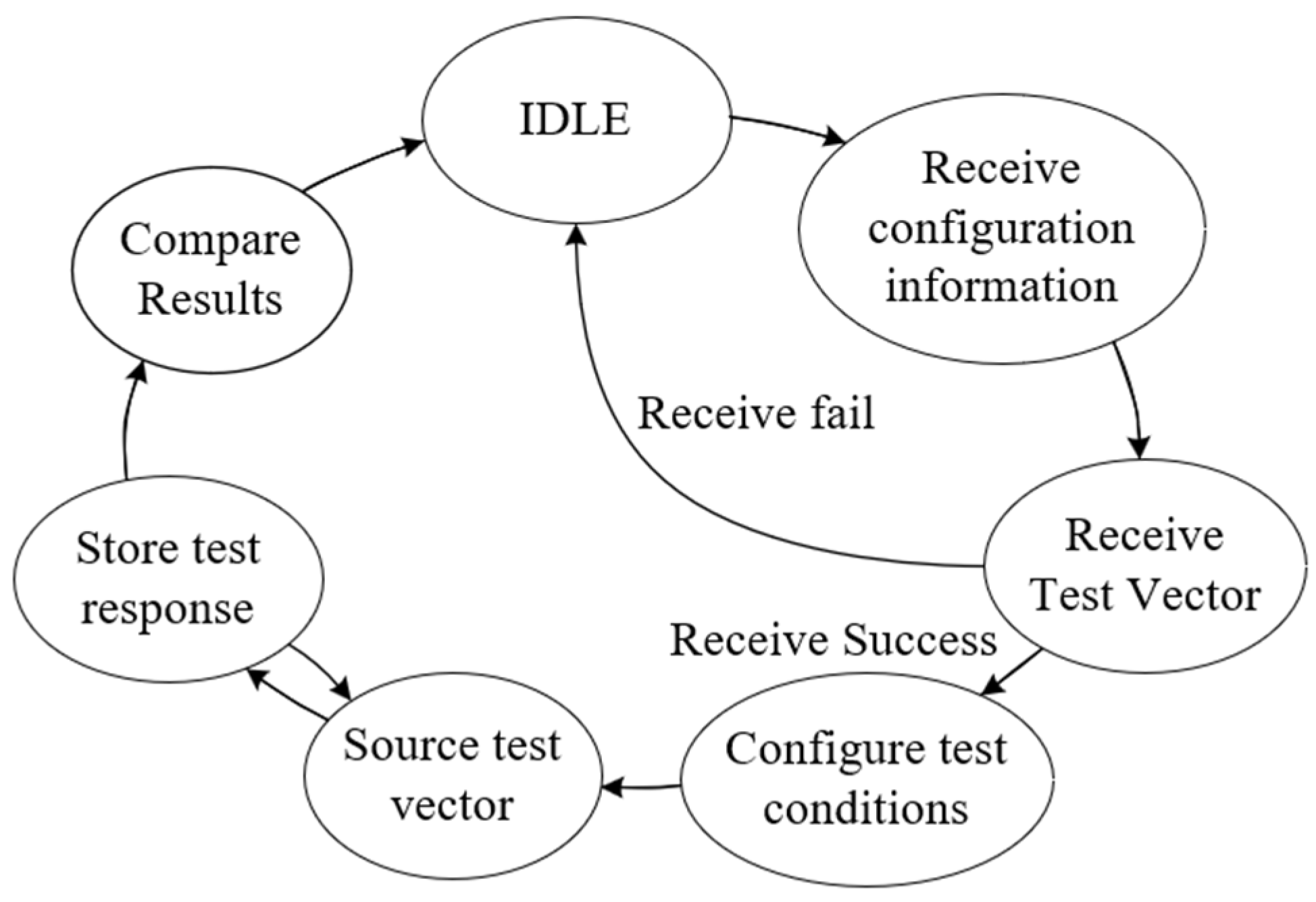
3.3.4. Test Control and Configuration
3.4. The Development Board
4. Validation and Evaluation
4.1. Chip Test and Analysis
4.1.1. Test Progress
4.1.2. Test Vectors and Results
4.2. Verification of Chip Performance
4.3. Performance of the FATE
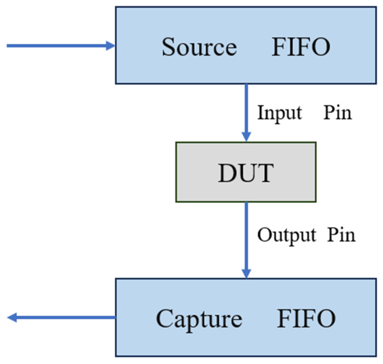
- Before the test vectors in the Source FIFO are completely consumed, new test vectors can be supplied for the next round;
- Before the Capture FIFO overflows, the Master DSP can read the test responses from the FIFO;
- During the data transmission between the Master DSP and FPGA, both the test vectors consumed by the test chip and the test responses generated do not exceed the set threshold depth.
5. Conclusions
Author Contributions
Funding
Data Availability Statement
Conflicts of Interest
References
- Wang, F.; Wang, L.; Yin, L. SoC chip UVM platform automated development system. China Integr. Circuit. 2023, 32, 72–77. [Google Scholar]
- Ishida, M.; Ichiyama, K. An ATE System for Testing RF Digital Communication Devices with QAM Signal Interfaces. IEEE Des. Test. 2016, 33, 15–22. [Google Scholar] [CrossRef]
- Song, X.; Wang, Y.; Chen, H. A Universal Auto Test Program Generation on Advantest V93000 ATE Platform. In Proceedings of the 2023 China Semiconductor Technology International Conference (CSTIC), Shanghai, China, 26–27 June 2023. [Google Scholar]
- Ionel, R.; Demian, P. A solution for integrating the Vector CANCase XL with the Teradyne Test Station ICT. In Proceedings of the International Symposium on Electronics and Telecommunications (ISETC), Timisoara, Romania, 8–9 November 2018. [Google Scholar]
- Shvachko, A.A.; Prokopenko, T.N.; Yanakova, E.S.; Kozlov, V.K. Digital Circuit Testing Methods: An Analysis of Modern Problems. In Proceedings of the Russian Young Researchers in Electrical and Electronic Engineering (ElConRus), St. Petersburg, Moscow, Russia, 26–29 January 2021. [Google Scholar]
- Lim, H.; Yun, H.; Kang, S. Scan Cell Modification for Intra Cell-Aware Scan Chain Diagnosis. IEEE Trans. Circuits Syst. II-Express Briefs 2022, 69, 4498–4502. [Google Scholar] [CrossRef]
- Kim, S.; Jang, S.; Kang, S. Scan Chain Architecture with Data Duplication for Multiple Scan Cell Fault Diagnosis. IEEE Trans. Comput-Aided Des. Integr. Circuits Syst. 2023, 42, 2717–2727. [Google Scholar] [CrossRef]
- Pathak, S.; Grover, A.; Pohit, M.; Bansal, N. LoCCo-Based Scan Chain Stitching for Low-Power DFT. IEEE Trans. Very Large Scale Integr. (VLSI) Syst. 2017, 25, 3227–3236. [Google Scholar] [CrossRef]
- Li, Y.H.; Lien, W.C.; Lin, I.C.; Lee, K.J. Capture-Power-Safe Test Pattern Determination for At-Speed Scan-Based Testing. IEEE Trans. Comput-Aided Des. Integr. Circuits Syst. 2014, 33, 127–138. [Google Scholar] [CrossRef]
- Ahmad, S.; Iqbal, K. X-Sand Filter: An X-Tolerant Response Compaction Technique for Faster-Than-At-Speed Testing. Mehran Univ. Res. J. Eng. Technol. 2020, 39, 353–364. [Google Scholar] [CrossRef]
- Hasib, O.A.T.; Savaria, Y.; Thibeault, C. Optimization of Small-Delay Defects Test Quality by Clock Speed Selection and Proper Masking Based on the Weighted Slack Percentage. IEEE Trans. Very Large Scale Integr. (VLSI) Syst. 2020, 28, 764–776. [Google Scholar] [CrossRef]
- Nawarathna, L.; Udugampola, N.; Yasawardhana, Y.; Weerasinghe, T.; Thayaparan, S. Low-Cost Automatic Test Equipment for Digital ICs Using DE0-Nano-Altera Cyclone IV FPGA. In Proceedings of the 3rd International Conference on Electrical, Control and Instrumentation Engineering (ICECIE), Kuala Lumpur, Malaysia, 27–27 November 2021. [Google Scholar]
- Rabakavi, B.; Siddamal, S. Design of High Speed, Reconfigurable Multiple ICs Tester using FPGA Platform. In Proceedings of the International Conference on Electrical, Electronics, Communication, Computer, and Optimization Techniques (ICEECCOT), Msyuru, India, 14–15 December 2018. [Google Scholar]
- Vanitha, K.; Sathiya Moorthy, C.A. Implementation of an integrated FPGA-based automatic test equipment and test generation for digital circuit. In Proceedings of the International Conference on Information Communication and Embedded Systems (ICICES), Chennai, India, 21–22 February 2013. [Google Scholar]
- Bayrakci, A.A. ELATE: Embedded low cost automatic test equipment for FPGA-based testing of digital circuits. In Proceedings of the 10th International Conference on Electrical and Electronics Engineering (ELECO), Bursa, Turkey, 30 November–2 December 2017. [Google Scholar]
- Che, W. FPGA-based memory test system design and test algorithm implementation. In Proceedings of the 3rd International Conference on Electronic Information Engineering and Computer (EIECT), Shenzhen, China, 17–19 November 2023. [Google Scholar]
- Wang, L.J.; Liu, X.L. Design and Implementation of an Automatic Test and Verification System for SoC. J. Phys. Conf. Ser. 2023, 2474, 012053. [Google Scholar] [CrossRef]
- Carvalho, D.D.; Sanches, B.; Carvalho, M.D.; Noije, W.V. A flexible stand-alone FPGA-based ATE for ASIC manufacturing tests. In Proceedings of the IEEE 19th Latin-American Test Symposium (LATS), Sao Paulo, Brazil, 12–14 March 2018. [Google Scholar]
- Luo, M.; Hu, C.M.; Yin, X.Y.; Wang, Y.H.; Zhao, Z.Y.; Hu, X. PASTE: FPGA-based portable at-speed scan test equipment. In Proceedings of the International Conference on Electronics and Integrated Circuit Technology, Shenzhen, China, 25–27 February 2021. [Google Scholar]
- Zhan, Z.H.; Hao, W.; Tian, Y.; Yao, D.; Wang, X. A Design of Versatile Image Processing Platform Based on the Dual Multi-coreDSP and FPGA. In Proceedings of the Fifth International Symposium on Computational Intelligence & Design, Hangzhou, China, 28–29 October 2012. [Google Scholar]
- LogiCORE IP Serial-RapidIO-Gen 2. Available online: https://www.xilinx.com/products/intellectual-property/ef-di-srio-gen2.html#overview (accessed on 12 March 2024).
- Xilinx, 7 Series FPGAs Data Sheet: Overview. Product Specification. DS180 (v2.6.1). 2020. Available online: https://www.xilinx.com/support/documentation/data_sheets/ds180_7Series_Overview.pdf (accessed on 2 December 2020).


| Interface | Software Overhead | Hardware Error Check | Transmission Distance | Packing Efficiency | Real-Time Performance |
|---|---|---|---|---|---|
| Ethernet | high | not support | long | 79% | normal |
| PCIE | medium | support | middle | 82% | normal |
| SRIO | low | support | middle | 95% | good |
| Port Name | I/O Port | Description |
|---|---|---|
| clk | I | 125 MHz clock |
| rst_n | I | Asynchronous low-level clear |
| tlast | I | The last data indicator signal |
| treq_id | I | SRIO device ID |
| treq_data | I | Master DSP input data |
| tvalid | I | Data valid information |
| fifo_id | O | FIFO ID |
| wr_data | O | FIFO write data bus |
| wr_en | O | FIFO write enable |
| Pin | ID |
|---|---|
| EMCD00 | 8′b00000001 |
| EMCD01 | 8′b00000010 |
| …… | …… |
| EMCD08 | 8′b00001001 |
| EMCD09 | 8′b00001010 |
| Test Vector | Length of Test Vectors | Number of Test Pins Required | Function Description |
|---|---|---|---|
| AC | Approximately 40 million bits | 52 | Based on different paths within the scan chain, transitions from 0 to 1 or from 1 to 0 are generated through test vectors, and the results of these transitions are captured using scan flip-flops at a set frequency. This process is used to verify whether the chip can operate normally at the specified frequency. |
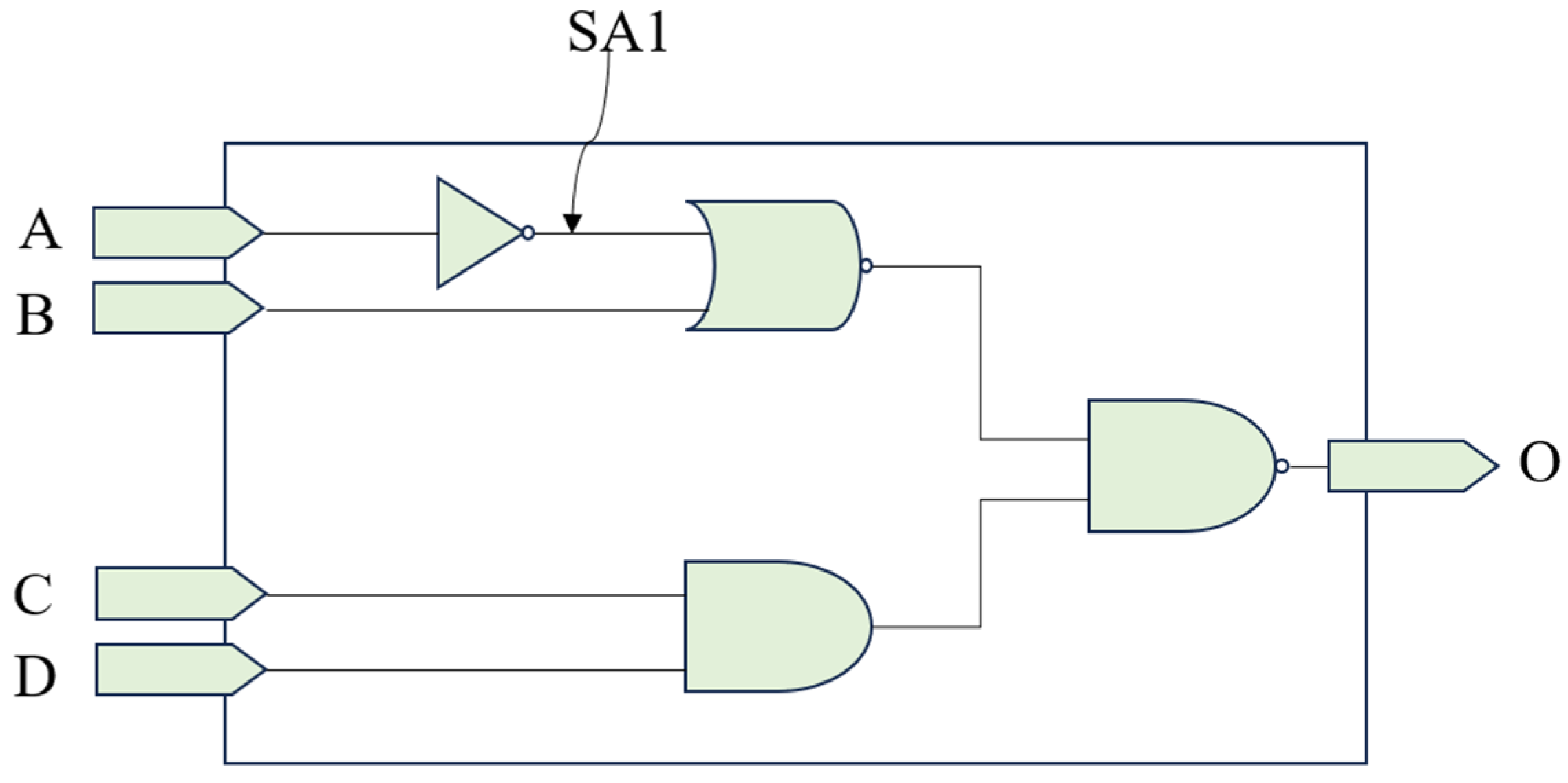
| DC | Approximately 10 million bits | 31 | Based on different positions within the scan chain, test vectors as shown in Figure 12 are generated to check for the presence of stuck faults at internal nodes. |
| 1100 | Approximately one hundred thousand bits | 31 | Numerous 1100 sequences are serially input and output within the scan chain, to check the completeness of the scan chain’s own channels. |
| Chip | Expected Result | Actual Result | Status of the Test |
|---|---|---|---|
| chip 1 | pass | pass | √ |
| chip 2 | pass | pass | √ |
| chip 3 | pass | pass | √ |
| chip 4 | pass | pass | √ |
| chip 5 | pass | pass | √ |
| chip 6 | pass | pass | √ |
| chip 7 | fail | fail | √ |
| chip 8 | pass | pass | √ |
| chip 9 | pass | pass | √ |
| chip10 | pass | pass | √ |
| Test Method | Test Frequency Range (MHz) | Result |
|---|---|---|
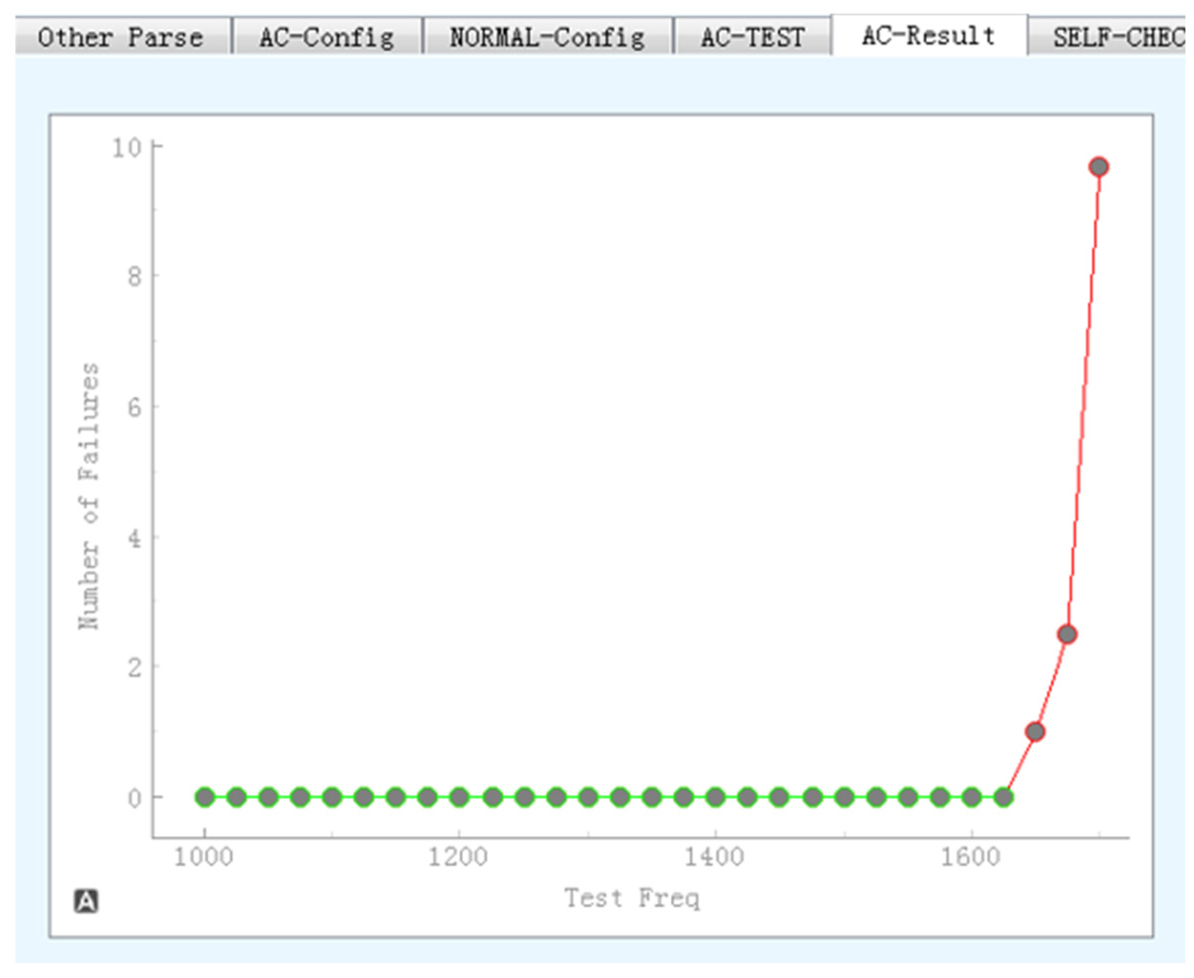
| FATE performance test | [1000, 1625] | pass |
| [1650, 1700] | fail | |
| Execute functional code | [1000, 1625] | pass |
| [1650, 1700] | fail |
| Work | Types of Chips Tested | Number of Test Channels | Supported Test Vector Length | Functional Test | Performance Test |
|---|---|---|---|---|---|
| [12] | NAND Gates | 16 | 2 KB | Support | Not Support |
| [18] | Chip with a design for test. | 16 | 200 MB | Support | Not Support |
| Our work | Chip with a design for test. | 160 | Unlimited | Support | Support |
| Work | Number of Test Channels | The Size of Resources Used by Each Channel | Test Vector Input Rate | Test Response Output Rate |
|---|---|---|---|---|
| PASTE [19] | 40 | 128 Kb | 1056 Mps | 800 Mps |
| Our work | 160 | 80 Kb | 16 Gps | 16 Gps |
Disclaimer/Publisher’s Note: The statements, opinions and data contained in all publications are solely those of the individual author(s) and contributor(s) and not of MDPI and/or the editor(s). MDPI and/or the editor(s) disclaim responsibility for any injury to people or property resulting from any ideas, methods, instructions or products referred to in the content. |
© 2024 by the authors. Licensee MDPI, Basel, Switzerland. This article is an open access article distributed under the terms and conditions of the Creative Commons Attribution (CC BY) license (https://creativecommons.org/licenses/by/4.0/).
Share and Cite
Zhang, J.; Liu, Z.; Hu, X.; Liu, P.; Hu, Z.; Kuang, L. FATE: A Flexible FPGA-Based Automatic Test Equipment for Digital ICs. Electronics 2024, 13, 1667. https://doi.org/10.3390/electronics13091667
Zhang J, Liu Z, Hu X, Liu P, Hu Z, Kuang L. FATE: A Flexible FPGA-Based Automatic Test Equipment for Digital ICs. Electronics. 2024; 13(9):1667. https://doi.org/10.3390/electronics13091667
Chicago/Turabian StyleZhang, Jin, Zhenghui Liu, Xiao Hu, Peixin Liu, Zhiling Hu, and Lidan Kuang. 2024. "FATE: A Flexible FPGA-Based Automatic Test Equipment for Digital ICs" Electronics 13, no. 9: 1667. https://doi.org/10.3390/electronics13091667
APA StyleZhang, J., Liu, Z., Hu, X., Liu, P., Hu, Z., & Kuang, L. (2024). FATE: A Flexible FPGA-Based Automatic Test Equipment for Digital ICs. Electronics, 13(9), 1667. https://doi.org/10.3390/electronics13091667