Abstract
A compound anti-interference control method based on a high-order nonlinear disturbance observer (HONDO) is proposed to address the impact of system disturbances on output voltage when applying the Buck–Boost converter in a microgrid to provide power to loads. Initially, the dynamic circuit model of the Buck–Boost converter is formulated, taking into account the system disturbance. Subsequently, HONDOs are designed to provide real-time estimates of uncertain factors in both the voltage loop and current loop of the circuit. These estimates are then utilized to design backstepping controllers aimed at effectively tracking the load output voltage set point. The simulation and experimental findings indicate that, when faced with load mutations, input voltage variations, and uncertainties in system parameters, the proposed compound anti-interference control method outperforms traditional control techniques by offering superior response speed, broader disturbance estimation capabilities, and enhanced dynamic performance of the Buck–Boost converter.
1. Introduction
Power electronics technology has been widely used in the construction of power systems based on new energy since the development of new energy and the continuous growth of industrial demand. Power electronics technology is currently a research hotspot in microgrid technology. A microgrid is a small-scale power supply system composed of distributed power supplies, energy storage devices, power supply equipment, loads, and other components [1,2].
As a switching power supply, a DC–DC converter can change the voltage output value and has the characteristics of small energy loss and compact device size [3], so it is widely used in the process of microgrid integration into the public network and power supply to loads. DC–DC converters provide different power characteristic voltages for different loads in the operation of a microgrid [4], and their control performance directly affects the stability of the microgrid system. Therefore, DC–DC converters play an important role in microgrid systems. The basic topologies of non-isolated DC–DC converters can be classified as Buck type, Boost type, Buck–Boost type, etc. The Buck–Boost converter is widely used in micro-grid systems because it can increase or decrease the output voltage with a wide voltage conversion range [5,6]. It is also widely used in electric vehicles, communication systems, industrial equipment, and other fields [7].
The Buck–Boost converter adjusts the output voltage by switching the power switch tube on and off. Its main control objective is to maintain a constant output voltage value under various transient conditions of load and power supply. However, in practical applications, the Buck–Boost converter is susceptible to environmental effects such as external input voltage variation, load uncertainty, internal resistive capacitance, and other parameter uncertainties, which can affect the system’s performance. In response to the above problems, experts have proposed many control methods in recent years, including PID control, fuzzy control, and sliding mode control [8,9]. The PID control method is simple in design and easy to implement in practical applications, but when there are disturbances in the system, it will affect the robustness of the system. Fuzzy control has a strong nonlinear adaptive ability [10], which can overcome the shortcomings of the traditional PID controller, but cannot overcome the influence of load uncertainty in the Buck–Boost converter. Sliding mode control [11] can solve the problem of model uncertainty, but it will lead to the chattering of output voltage [12], and variable switching frequency will lead to electromagnetic interference [13], so the system has a steady-state error. This approach still does not meet the control performance requirements of the system. These methods can improve the control performance of the system in different aspects, but they cannot perform active anti-disturbance control over the system disturbances. Disturbance observer-based control (DO) is currently one of the most effective methods for suppressing disturbances [14]. Disturbance observers can estimate system uncertainty and disturbances as lumped disturbances, thereby improving system tracking performance without using large feedback gains. Chen proposed a design method for nonlinear disturbance observer (NDO) [15]. Yang et al. utilized the control method of NDO to solve the robust control problem of nonlinear systems with disturbances and uncertainties [16]. Wang et al. designed a sliding mode control law based on DO for boost converters, achieving asymptotic stability of output voltage under disturbance [17]. The literature [18] proposes a new robust proportional integral derivative controller design method, which solves the disturbance suppression problem of nonminimum phase DC–DC boost converters operating in continuous conduction mode. Errouissi et al. proposed a DO-based output voltage regulation method for boost converters. The controller consists of a combination of linearized feedback control and disturbance observer, which alleviates the impact of transient control saturation. However, there is a large overshoot of the output voltage during system disturbances [19]. The literature [20] proposes an adaptive control method based on a Buck–Boost converter, which improves the overall control effect of the system by updating the switching time adjustment parameters of the switching devices in real-time. The literature [21] proposes a robust passivity-based control strategy to mitigate the instability impact of DC–DC boost power converters providing constant power and voltage loads in DC microgrid systems. Saadat et al. used an adaptive backstepping control method to improve the robustness of parameter estimation and reduce the negative impact of interference factors on the estimation quantity [22]. However, the above methods did not consider the uncertainty of inductance and capacitance parameters in the model. When the inductance and capacitance parameters do not match the nominal values, it will have a certain impact on the system. At the same time, it was not considered that in certain application scenarios, disturbance types may have the influence of higher-order disturbances in addition to step disturbances.
This paper proposes a composite disturbance rejection control method based on high-order nonlinear disturbance observer (HONDO) to address the problem of unstable output voltage caused by system disturbances in Buck–Boost converters. The main contributions of this paper are as follows:
- (1)
- Consider system disturbances and parameter uncertainties, establish system dynamic equations, and introduce nominal values to simplify the system model. Design dual high-order nonlinear disturbance observers for voltage and current loops based on dynamic equations, estimate the disturbance of the Buck–Boost circuit in rea-time, and provide compensation, thereby improving the system’s anti-interference ability against high-order disturbances;
- (2)
- Design a backstepping disturbance rejection controller based on a high-order nonlinear disturbance observer to achieve good tracking of the system output voltage reference value and improve system response speed;
- (3)
- By combining a dual high-order nonlinear disturbance observer with a backstepping controller to form a composite disturbance rejection controller, the proposed control method can eliminate the influence of model parameter uncertainty, have a wider disturbance rejection range, and effectively improve the robustness and dynamic performance of the Buck–Boost converter in microgrid applications.
2. Modeling of the Buck–Boost Converter
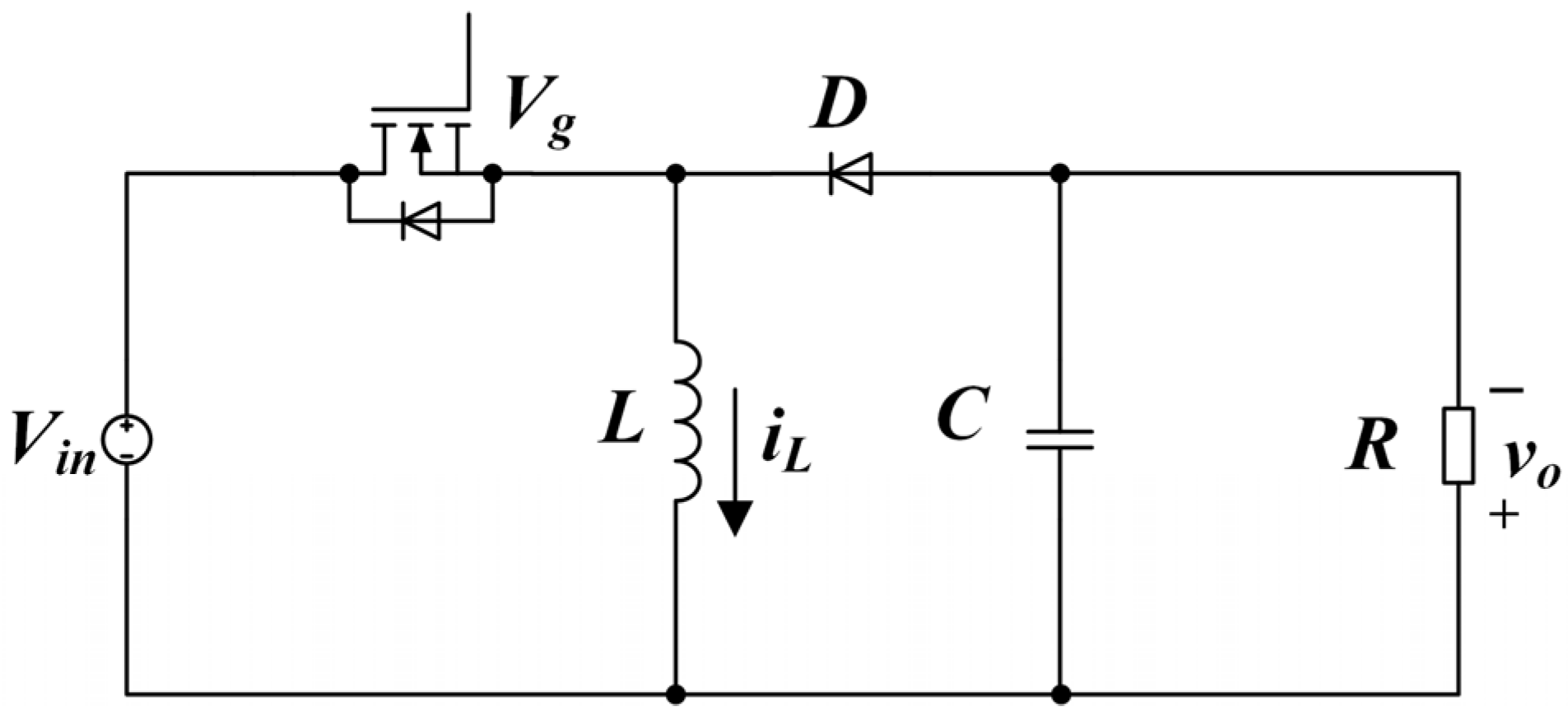
The circuit topology of the Buck–Boost converter based on PWM is shown in Figure 1. is the input voltage, is the switching tube, D is the relaying diode, L is the circuit inductance, C is the circuit capacitance, R is the circuit load resistance, is the inductive current, and is the load output voltage.
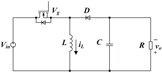
Figure 1.
Circuit topology of the Buck–Boost converter.
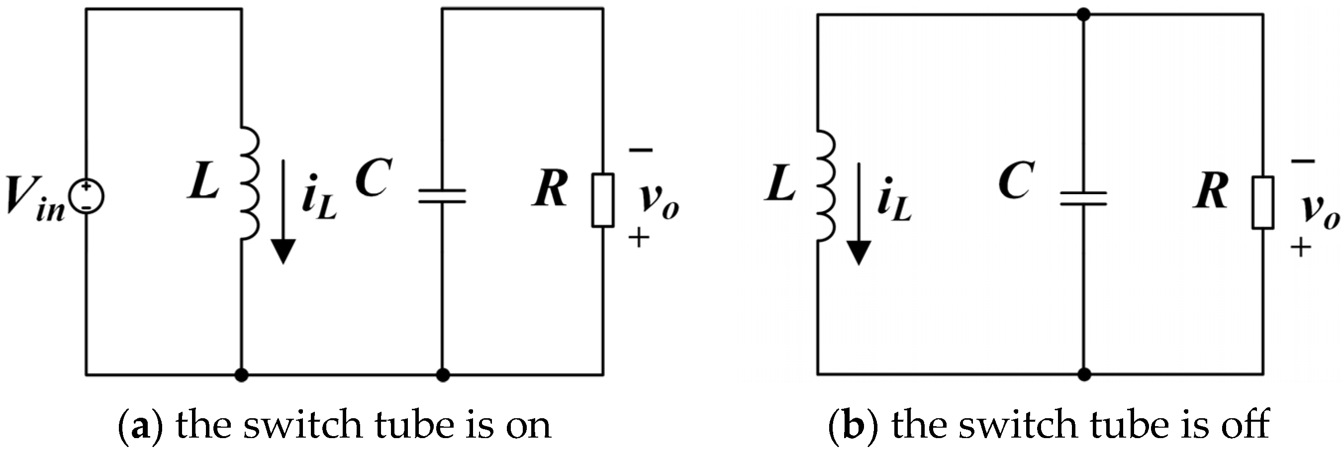
The Buck–Boost converter circuit is modeled using the state space averaging method in continuous inductance mode. When the switch tube () is switched on, the equivalent circuit diagram of the Buck–Boost converter is shown in Figure 2a. The power supply () is supplied at both ends of the inductor, the inductor current () increases linearly, the inductor (L) stores energy, the diode (D) is cut off, and the output voltage at the right end is maintained by the discharge of capacitor C. The circuit model is as follows:
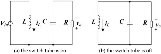
Figure 2.
Equivalent circuit of the Buck–Boost converter.
When the switch tube () is disconnected, the equivalent circuit diagram of the Buck–Boost converter is shown in Figure 2b. The inductor current () flows through the capacitor (C) and the load resistance (R), the diode (D) is switched on, the inductor (L) is discharged, and the capacitor (C) is charged. At this time, the circuit model is as follows:
Therefore, the average switching model can be written as follows:
where is the duty cycle.
Considering the load resistance in the Buck–Boost circuit, the dynamic model of the circuit can be expressed as follows:
The duty cycle () can be obtained from Equation (4):
By inputting the voltage reference value () into Equation (4), the ideal inductance current nominal value of the Buck–Boost converter in a stable state can be obtained:
In practical applications, considering the input voltage () and load resistance (R) in Buck–Boost circuits are subject to various external uncertainties, as well as the uncertainty of inductance (L) and capacitance (C) parameters. Let , , , and be the nominal values of input voltage (), resistance (R), inductance (L), and capacitance ©, respectively. Express as the nominal value . The disturbance caused by the voltage loop channel is represented as , and the disturbance caused by the current loop channel is represented as . The dynamic model (3) of the circuit can be expressed as follows:
where , , , and . The expressions for and are as follows:
where , , , and .
3. Design of High-Order Nonlinear Disturbance Observer
3.1. First-Order Nonlinear Disturbance Observer
Design disturbance observers based on system models to estimate disturbances in the system. Consider the design of disturbance observers for different types of disturbances. When the disturbance is constant, design a first-order nonlinear disturbance observer based on the system model (7) to estimate the disturbance in the system. The form of the voltage loop nonlinear disturbance observer NDO1 is as follows:
The NDO2 form of the current loop nonlinear disturbance observer is as follows:
where and are the estimated values of and disturbances, and are the estimated values of , and , , and are the observer gains, and , .
The disturbance estimation errors and are defined as follows:
Substituting the disturbance observer Equations (9) and (10) into the above equation yields
Organized disturbance estimation error:
When the disturbances and are constant and , , this proves that the error system is asymptotically stable, indicating that the disturbance observer can asymptotically track the disturbance. By designing disturbance compensation gains ( and ) reasonably, it can be ensured that the output channel is not affected by disturbances during a steady state.
3.2. Second-Order Nonlinear Disturbance Observer
When the disturbance s is a slope disturbance as follows:
where and are unknown constants.
According to the system model (7), design second-order nonlinear disturbance observers for voltage and current loops as follows:
where and are the disturbance estimates and , respectively. and are the observer gains, and , .
The disturbance estimation errors and are defined as follows:
Combining Equations (15)–(17), the disturbance estimation error can be obtained:
When the disturbance is a slope (), selecting appropriate and (), the estimation error will converge to zero.
3.3. High-Order Nonlinear Disturbance Observer
When the disturbance is a high-order disturbance as follows:
where is an unknown constant.
According to the system model (7), design the voltage loop HONDO1 and current loop HONDO2 as follows:
where and are disturbance estimates for and , respectively. and are observer gains, and , , , .
The disturbance estimation errors and are defined as follows:
By combining Equations (20)–(23), the disturbance estimation error can be obtained:
When the disturbance satisfies Equation (20) and , the error dynamics equation can be obtained:
Select the parameters and such that the left polynomial of (26) is Hurwitz (the real numbers of the zeros of the polynomials are negative), and the estimation error will converge to zero.
4. Backstepping Controller Based on High-Order Nonlinear Disturbance Observer
To prevent the inductance current from losing control in a single closed-loop control system, a dual closed-loop control method is adopted. The control strategy proposed in this paper consists of two disturbance observers and two backstepping controllers, which are used to estimate system disturbances and regulate output voltage, respectively. By designing two disturbance observers to estimate the disturbances in the inductance current and output voltage channels in real-time and using the estimated values of HONDO to design a backstepping controller, the output voltage can accurately track its reference voltage and improve the robustness of the system. The backstepping control structure based on a high-order nonlinear disturbance observer is shown in Figure 3. In the figure, HONDO1 is the voltage loop high-order nonlinear disturbance observer, HONDO2 is the current loop high-order nonlinear disturbance observer, is the output voltage error, is the inductance current error, and is the output voltage set value.
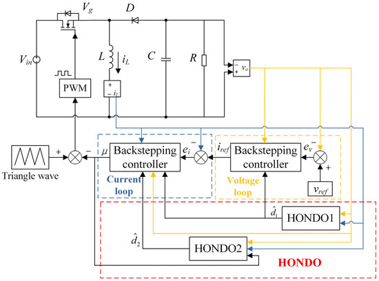
Figure 3.
The control structure of the backstepping control based on high-order nonlinear disturbance observer.
Backstepping controllers exhibit significant advantages when dealing with nonlinear systems, as they enable a layer-by-layer design approach where control laws are recursively constructed in reverse order to ensure the system states evolve along desired trajectories, thereby effectively overcoming nonlinear challenges. The main control objective of the backstepping controller is to control the duty cycle of the Buck–Boost converter switch to adjust the output voltage so that the output voltage can accurately track its reference voltage.
Let and , taking the derivative of yields:
Choose the Lyapunov function as follows:
Differentiate Equation (28) to obtain
In order to stabilize ev, the control quantity iref can be designed as follows:
where k1 > 0 is the control coefficient.
According to Equation (29), can be organized as
Taking the derivative of the inductance current error to obtain
Choose the Lyapunov function as follows:
In order to stabilize , the control quantity can be designed as
where k2 > 0 is the control coefficient.
Differentiate Equation (33) to obtain
According to Equations (33) and (35), it can be seen that V2 is positive definite and is negative definite, and the error system is stable at this time.
By inputting the disturbance estimation values of the high-order nonlinear disturbance observer into Equations (30) and (34), the voltage loop and current loop control rates are obtained, respectively:
5. Simulation and Experimental Verification
To verify the effectiveness of the control strategy proposed in this article, simulation verification was conducted based on the Matlab/Simulink platform. Apply the HONDO composite control method to control the output voltage of the Buck–Boost circuit, estimate the disturbance in the output voltage and inductor current in real-time, and provide compensation. Firstly, verify the anti-interference performance of the proposed backstepping controller based on HONDO (abbreviated as HONDO-B). Then, compare the proposed method with backstepping control based on disturbance observer (abbreviated as DO-B) in the following three situations: (1) sudden load change; (2) input voltage sudden change; (3) the parameters of inductance and capacitance are uncertain. The specific parameters of the Buck–Boost converter system are shown in Table 1.

Table 1.
Parameters of the Buck–Boost converter.
The controller parameters of the composite control method proposed in the simulation experiment are l131 = l231 = 550, l132 = l232 = 1200, l133 = l233 = 8000, k1 = 20, k2 = 1000.
5.1. Simulation Results
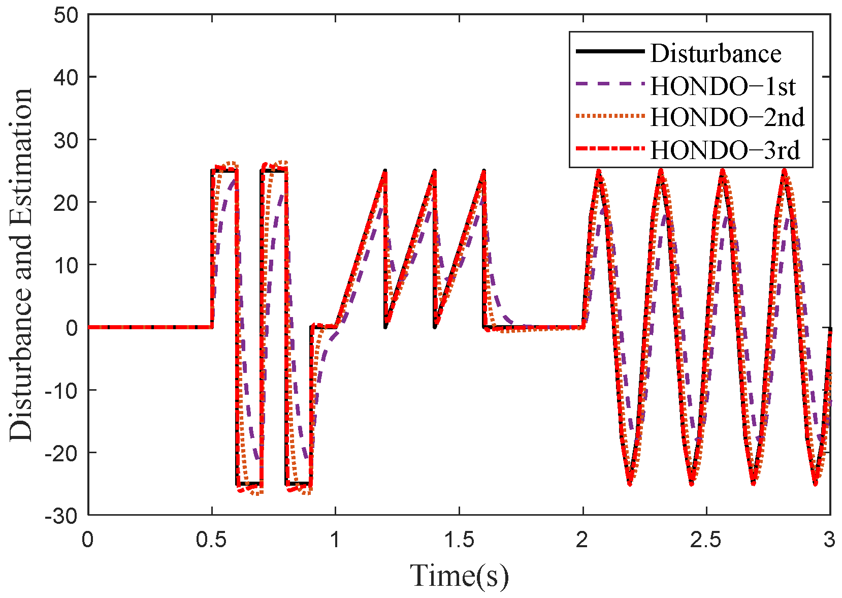
To verify the disturbance estimation ability of the proposed HONDO control strategy, simulation comparisons were conducted on three different orders of HONDO under three different disturbance types. Figure 4 shows the comparison of estimation errors for first-order, second-order, and third-order HONDO, and Figure 5 shows the output voltage waveform. It can be seen that the amplitude of first-order NDO is the largest, while that of third-order NDO is the smallest. The results indicate that the higher the order of HONDO, the stronger its anti-interference ability.

Figure 4.
Comparison of estimation performance of d1 and d2 among the first-order, second-order, and third-order NDOs.
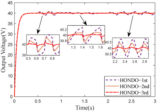
Figure 5.
Output voltage.
Considering the sudden change in load resistance during actual operation, verify the ability of the proposed control method to suppress load disturbances and compare the control algorithm proposed in this paper with DO-B. The simulation time is 1 s, and at t = 0.3 s, the load increases from 50 Ω to 75 Ω. At t = 0.7 s, the load decreases from 75 Ω to 50 Ω. The response curve of the load output voltage is shown in Figure 6. When the load suddenly increases, the absolute integration (IAE) of the output voltage error between the control algorithm proposed in this article and DO-B is 0.0067 V and 0.0923 V, respectively. When the load suddenly drops, the IAE of the output voltage is 0.0048 V and 0.0569 V, respectively. It can be seen that the control method proposed in this article has a shorter time for the output voltage to recover to steady-state value and a smaller overshoot when there is load disturbance in the system. The system output voltage can quickly track the reference value and has strong anti-interference performance.
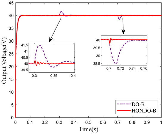
Figure 6.
Output voltage under load mutation.
Considering the sudden change in input voltage during actual operation, verify the ability of the dual closed-loop disturbance observer control method to suppress system input voltage disturbances. The simulation time is 1 s. At t = 0.3 s, the input voltage increases from 60 V to 90 V. At t = 0.7 s, the input voltage decreases from 90 V to 60 V. The load output voltage response curve is shown in Figure 7. In the case of a sudden increase in input voltage, the IAE of the two control methods is 0.0052 V and 0.0605 V, respectively. The IAE under sudden decrease in input voltage is 0.0046 s and 0.0399 s, respectively. It can be seen that the control method proposed in this article has a faster convergence speed, smaller overshoot or overshoot, and stronger anti-interference performance when there is input voltage disturbance in the system.
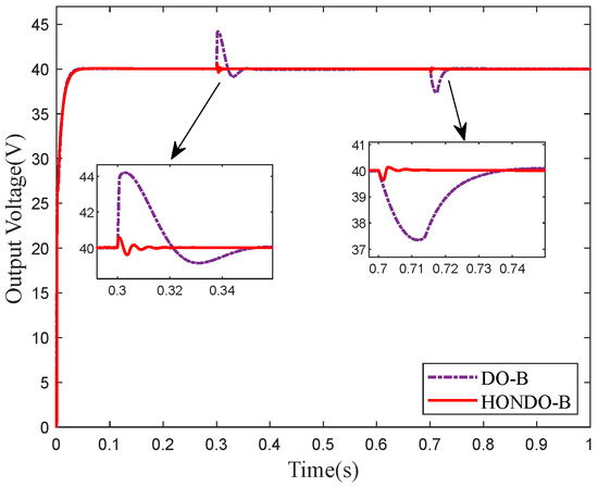
Figure 7.
Output voltage under input voltage mutation.
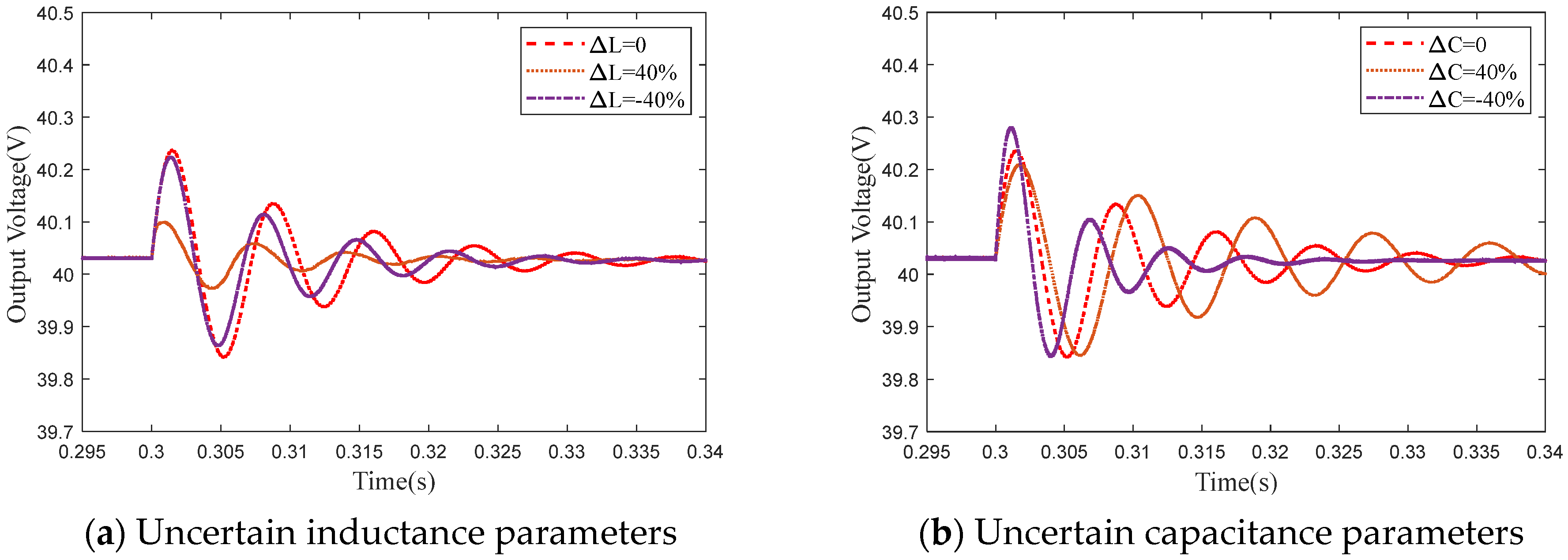
Considering that the actual inductance and capacitance parameters may be affected by operating time or environmental factors, and the system may be affected by model uncertainty, the robustness of the proposed control method with uncertain inductance and capacitance parameters is verified. Increase the inductance and capacitance values by 40% and decrease them by 40%, respectively. Figure 8 shows the output voltage response waveforms corresponding to different inductance and capacitance values when the load suddenly changes. Figure 8a shows the output voltage waveform diagram of different inductance parameters under sudden load changes, and Figure 8b shows the output voltage waveform diagram of different capacitance parameters under sudden load changes. From Figure 8, it can be seen that the proposed control method can eliminate the influence of model parameter uncertainty, maintain the stable output of the system, and quickly adjust back to a steady state in case of sudden load changes.
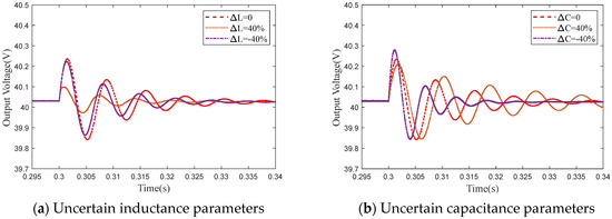
Figure 8.
Output voltage under uncertain inductance and capacitance parameters during sudden load changes.
5.2. Experimental Results
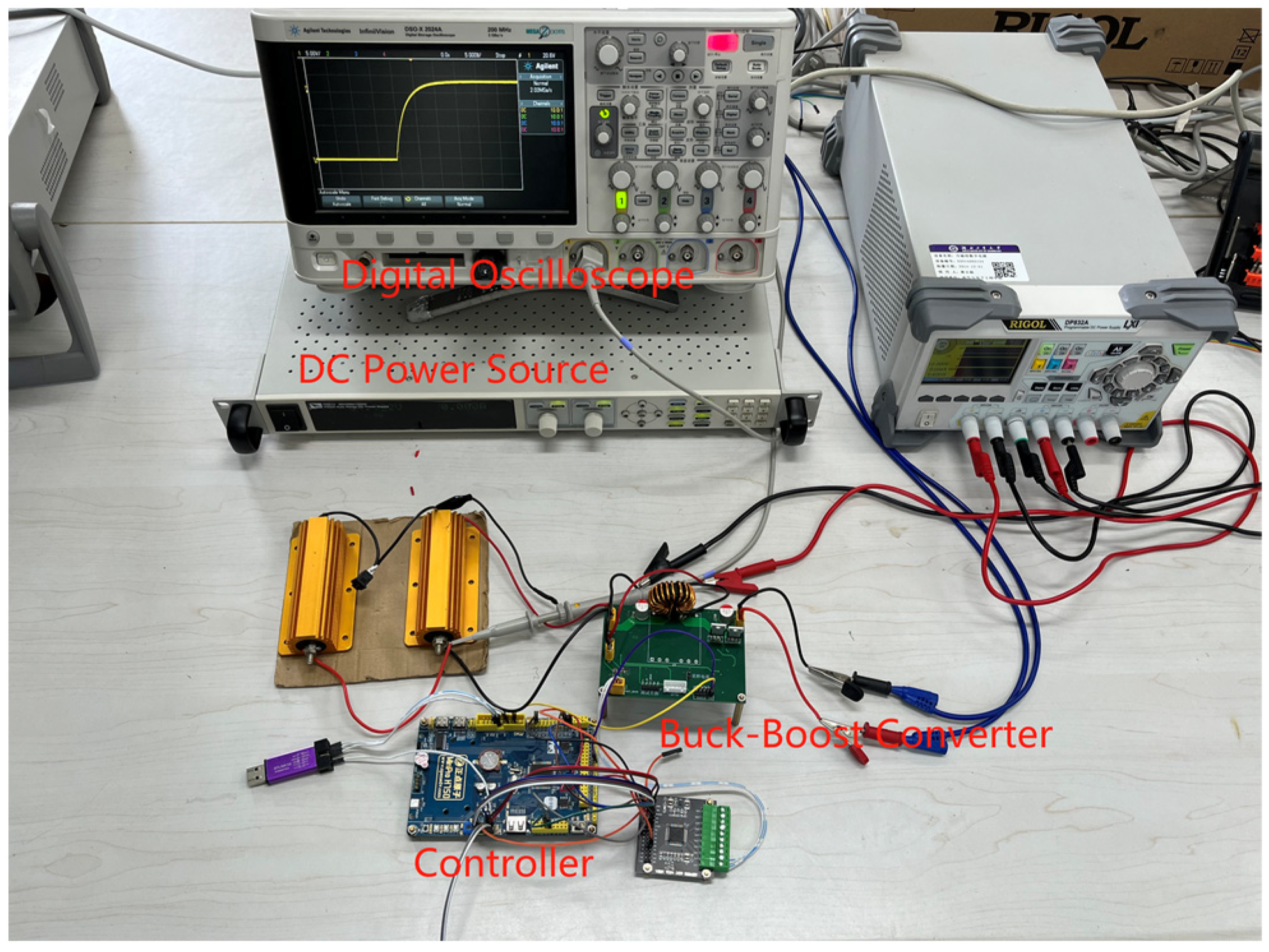
The experimental platform shown in Figure 9 was constructed to further verify the accuracy and reliability of the method. This system includes a DC voltage source, an STM32 development board, a Buck–Boost converter main circuit, and a digital oscilloscope. The experimental platform mainly consists of a DC voltage source, an STM32 development board, a Buck–Boost converter main circuit, and a digital oscilloscope. The system controller adopts the STM32 series microcontroller for signal acquisition, uses a Tektronix MSO 2024B oscilloscope to measure the voltage at both ends of the load, and combines the RP1025D differential probe and RP1001C current probe to detect the load voltage and inductance current. The input voltage of the Buck–Boost converter is 40 V, the reference output voltage is 30 V, the switching frequency is 50 kHz, the inductance value is 275 µH, the capacitance value is 47 µF, and the resistance value is 30 Ω. Using the HONDO-B control method proposed in this article, the output voltage of the Buck–Boost circuit is controlled, and disturbances in the output voltage and inductance current are estimated in real-time and compensated. Compare the proposed method with the DO-B method in two scenarios: sudden load changes and input voltage changes.

Figure 9.
Experimental platform.
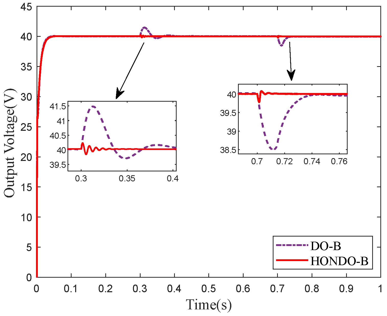
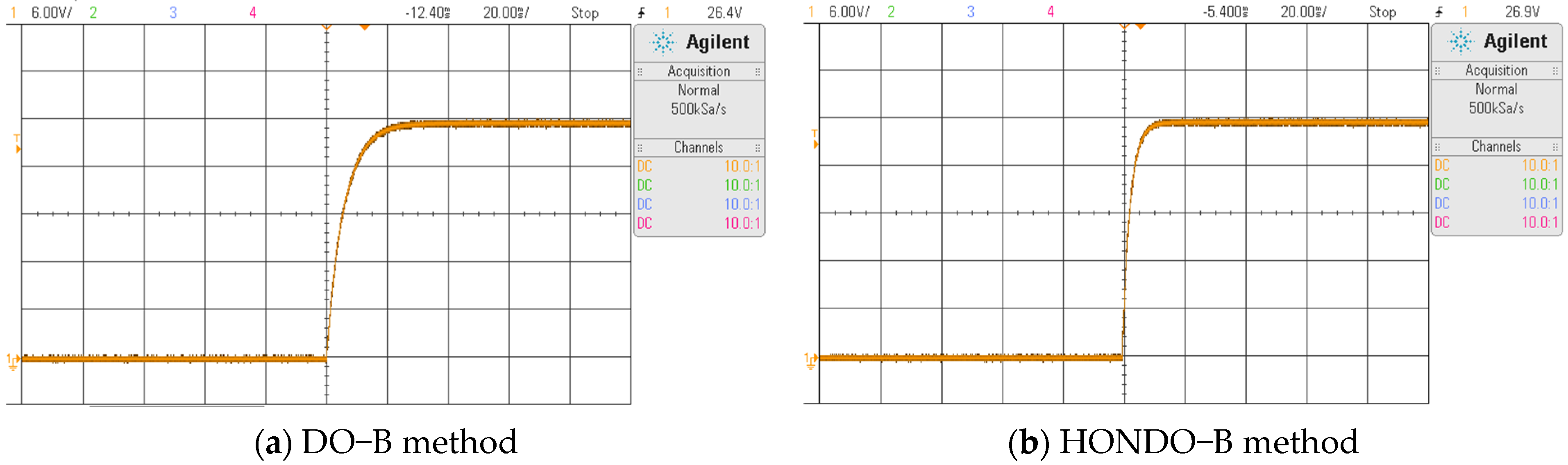
Firstly, measure the power of response. Figure 10 shows the transient response curve of the Buck–Boost converter, where Figure 10a shows the DO-B method and Figure 10b shows the HONDO-B method. From the figure, it can be seen that the output voltage rise times of DO-B and the proposed method are 0.03 s and 0.01 s, respectively. The proposed method can obtain a fast transient response.
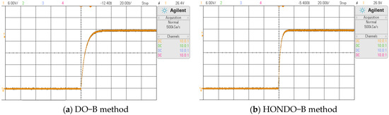
Figure 10.
Transient response curve.
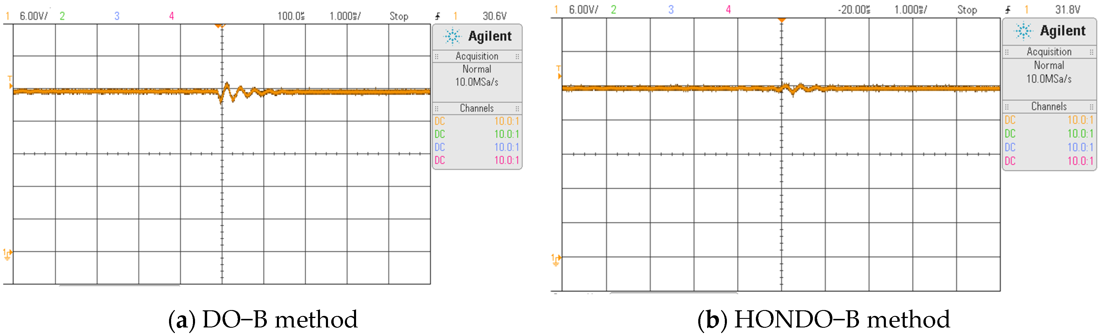
The first system testing is a load resistance variation. Verify the ability of the dual closed-loop HONDO-B control method to suppress load disturbances and reduce the load from 30 Ω to 15 Ω. The response curve of the load output voltage is shown in Figure 11. Figure 11a,b show the output voltage under DO-B control and HONDO-B control, respectively. The performance indicators of voltage regulation time and output voltage under two types of control are shown in Table 2. It can be seen that the control method proposed in this article has a shorter time for the output voltage to recover to steady-state value and a smaller overshoot when there is load disturbance in the system. The system output voltage can quickly track the reference value and has strong anti-interference performance.
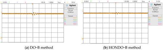
Figure 11.
Output voltage under load mutation.
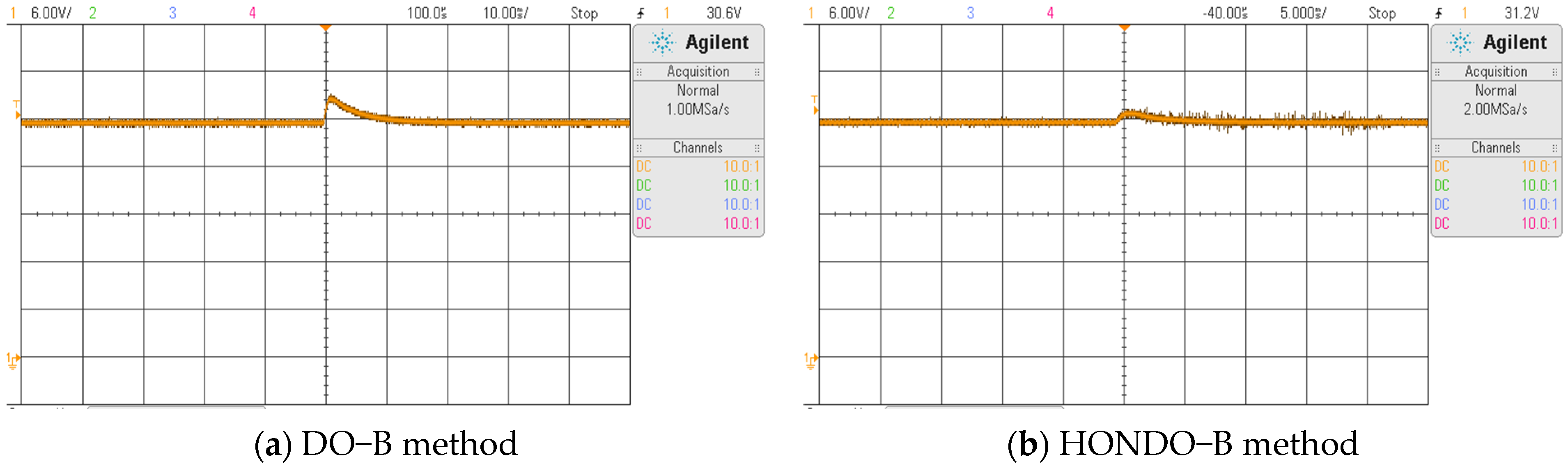
Table 2.
Performance indicators under input voltage mutation.
The next system testing is the input voltage variation. Verify the ability of the dual closed-loop HONDO-B control method to suppress system input voltage disturbances, increasing the input voltage from 40 V to 45 V. The load output voltage response curve is shown in Figure 12, where Figure 12a,b represent the output voltage under DO-B and HONDO-B control, respectively. The control performance indicators of the two control methods under sudden input voltage changes are shown in Table 2. From the comparison between the response curve in Figure 12 and the data in Table 2, it can be seen that the control method proposed in this paper converges faster, has smaller overshoot or overshoot, and stronger anti-interference performance when there is input voltage disturbance in the system.
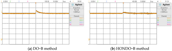
Figure 12.
Output voltage under input voltage mutation.
6. Conclusions
This article focuses on the impact of system disturbances on the output voltage of Buck–Boost converters when supplying power to loads in microgrids. Based on a disturbance observer, this paper proposes a backstepping disturbance rejection control method for Buck–Boost converters using a dual closed-loop, high-order nonlinear disturbance observer. A dynamic mathematical model of the Buck–Boost converter was established, and nominal values were introduced to simplify the mathematical model of the circuit. Real-time estimation and compensation of system disturbances are achieved through a high-order nonlinear disturbance observer combined with a backstepping controller to achieve voltage tracking control. The superiority of the composite control method proposed in this paper was verified through simulation and experiments. The experimental results demonstrate that the proposed control method effectively tracks the system’s output voltage reference value. Compared to DO-B, the proposed control method exhibits a faster response speed, as evidenced by a reduction in the transient response time by 0.02 s. Moreover, under load disturbance, both overshoot and down impulse decrease by 0.81 V and 1.08 V, respectively. When the input voltage changes, the overshoot decreases by 1.95 V. These results indicate that HONDO-B outperforms other control methods in enhancing the system’s response speed and anti-interference ability. Future research will focus on exploring the parameter tuning method for the composite controller to derive more precise controller parameters, thereby further enhancing the system’s robustness.
Author Contributions
Conceptualization, Y.C. and W.Y.; methodology, W.Y.; software, W.Y.; validation, W.Y., M.L. and F.Z.; formal analysis, Y.C. and W.Y.; investigation, W.H., F.Z. and G.Z.; resources, F.Z. and W.H.; writing—original draft preparation, W.Y.; writing—review and editing, Y.C. and W.Y.; visualization, W.Y. and G.Z.; supervision, M.L., W.H. and G.Z. All authors have read and agreed to the published version of the manuscript.
Funding
This research was funded by the National Natural Science Foundation of China under grant number 61903129 and the Hubei University of Technology Doctoral Research Project under grant number BSQD2020012.
Data Availability Statement
Data are contained within the article.
Conflicts of Interest
The authors declare no conflicts of interest.
References
- Heidary, J.; Gheisarnejad, M.; Khooban, M.H. Stability Enhancement and Energy Management of AC-DC Microgrid based on Active Disturbance Rejection Control. Electr. Power Syst. Res. 2023, 217, 109105. [Google Scholar] [CrossRef]
- Zhou, K.; Qiu, X.; Song, Y.; Jin, Q.; Mo, Z. Research on Coordinated DC voltage Control Strategy of DC Microgrid based on Photovoltaic Power Generation System. J. Phys. Conf. Ser. 2022, 2246, 012066. [Google Scholar] [CrossRef]
- Martinez-Trevino, B.A.; El Aroudi, A.; Valderrama-Blavi, H.; Cid-Pastor, A.; Vidal-Idiarte, E.; Martinez-Salamero, L. PWM nonlinear control with load power estimation for output voltage regulation of a boost converter with constant power load. IEEE Trans. Power Electron. 2020, 36, 2143–2153. [Google Scholar] [CrossRef]
- Guo, Q.; Bahri, I.; Diallo, D.; Berthelot, E. Model predictive control and linear control of DC-DC boost converter in low voltage DC microgrid: An experimental comparative study. Control Eng. Pract. 2023, 131, 105387. [Google Scholar] [CrossRef]
- Rajamani, M.P.E.; Rajesh, R.; Iruthayarajan, M.W. A PID control scheme with enhanced non-dominated sorting genetic algorithm applied to a non-inverting buck-boost converter. Sadhana Acad. Proc. Eng. Sci. 2022, 47, 222. [Google Scholar] [CrossRef]
- Molina-Santana, E.; Gonzalez-Montañez, F.; Liceaga-Castro, J.U.; Jimenez-Mondragon, V.M.; Siller-Alcala, I. Modeling and Control of a DC-DC Buck–Boost Converter with Non-Linear Power Inductor Operating in Saturation Region Considering Electrical Losses. Mathematics 2023, 11, 4617. [Google Scholar] [CrossRef]
- Kasicheyanula, S.; John, V. Adaptive control strategy for ultracapacitor based bidirectional dc-dc converters. IEEE Trans. Ind. Appl. 2018, 55, 1717–1728. [Google Scholar] [CrossRef]
- Cortajarena, J.A.; Barambones, O.; Alkorta, P.; Cortajarena, J. Sliding mode control of an active power filter with photovoltaic maximum power tracking. Int. J. Electr. Power Energy Syst. 2019, 110, 747–758. [Google Scholar] [CrossRef]
- Soriano-Sánchez, A.G.; Rodríguez-Licea, M.A.; Pérez-Pinal, F.J.; Vázquez-López, J.A. Fractional-Order Approximation and Synthesis of a PID Controller for a Buck Converter. Energies 2020, 13, 629. [Google Scholar] [CrossRef]
- Rajendran, S.; Thangavel, V.; Krishnan, N.; Prabaharan, N. DC Link Voltage Enhancement in DC Microgrid Using PV Based High Gain Converter with Cascaded Fuzzy Logic Controller. Energies 2023, 16, 3928. [Google Scholar] [CrossRef]
- Zheng, S.; Qi, M.; Shu, Y.; Wang, Y.; Lang, J. Non-singular terminal sliding mode control strategy for DC/DC Boost converter system using a finite-time convergent observer. IET Power Electron. 2022, 15, 1868–1876. [Google Scholar] [CrossRef]
- Samantaray, J.; Chakrabarty, S.; Bartoszewicz, A. Advanced discrete-time sliding mode control with fast output sampling and its application to buck converter. Automatica 2023, 149, 110802. [Google Scholar] [CrossRef]
- Abjadi, N.; Goudarzian, A.; Markadeh, G.R.A.; Valipour, Z. Reduced-Order Backstepping Controller for POESLL DC–DC Converter Based on Pulse Width Modulation. Iran. J. Sci. Technol. Trans. Electr. Eng. 2019, 43, 219–228. [Google Scholar] [CrossRef]
- Chaudhari, S.; Shendge, P.D.; Phadke, S.B. Disturbance Observer Based Controller Under Noisy Measurement for Tracking of nDOF Uncertain Mismatched Nonlinear Interconnected Systems. IEEE/ASME Trans. Mechatron. 2020, 25, 1600–1611. [Google Scholar] [CrossRef]
- Chen, W.H. Disturbance observer based control for nonlinear systems. IEEE/ASME Trans. Mechatron. 2004, 9, 706–710. [Google Scholar] [CrossRef]
- Yang, J.; Li, S.; Yu, X. Sliding-Mode Control for Systems With Mismatched Uncertainties via a Disturbance Observer. IEEE Trans. Ind. Electron. 2013, 60, 160–169. [Google Scholar] [CrossRef]
- Wang, R.; Mei, L.; Zhang, G. Disturbance Observer-Based Sliding Mode Control for DC-DC Boost Converter. In Proceedings of the 2018 IEEE 3rd Advanced Information Technology, Electronic and Automation Control Conference (IAEAC), Chongqing, China, 12–14 October 2018. [Google Scholar] [CrossRef]
- Kobaku, T.; Jeyasenthil, R.; Sahoo, S.; Dragicevic, T. Experimental Verification of Robust PID Controller Under Feedforward Framework for a Nonminimum Phase DC–DC Boost Converter. IEEE J. Emerg. Sel. Top. Power Electron. 2021, 9, 3373–3383. [Google Scholar] [CrossRef]
- Errouissi, R.; Shareef, H.; Viswambharan, A.; Wahyudie, A. Disturbance Observer-Based Control for DC-DC Boost Converter. In Proceedings of the 2021 IEEE Industry Applications Society Annual Meeting (IAS), Vancouver, BC, Canada, 10–14 October 2021; pp. 1–6. [Google Scholar]
- Mollaee, H.; Ghamari, S.M.; Saadat, S.A.; Wheeler, P. A novel adaptive cascade controller design on a buck–boost DC–DC converter with a fractional-order PID voltage controller and a self-tuning regulator adaptive current controller. IET Power Electron. 2021, 14, 1920–1935. [Google Scholar] [CrossRef]
- Hassan, M.A.; Su, C.L.; Chen, F.Z.; Lo, K.Y. Adaptive Passivity-Based Control of DC-DC Boost Power Converter Supplying Constant Power and Constant Voltage Loads. IEEE Trans. Ind. Electron. 2021, 69, 6204–6214. [Google Scholar] [CrossRef]
- Saadat, S.A.; Ghamari, S.M.; Mollaee, H. Adaptive backstepping controller design on Buck converter with a novel improved identification method. IET Control. Theory Appl. 2022, 16, 485–495. [Google Scholar] [CrossRef]


Disclaimer/Publisher’s Note: The statements, opinions and data contained in all publications are solely those of the individual author(s) and contributor(s) and not of MDPI and/or the editor(s). MDPI and/or the editor(s) disclaim responsibility for any injury to people or property resulting from any ideas, methods, instructions or products referred to in the content. |
© 2024 by the authors. Licensee MDPI, Basel, Switzerland. This article is an open access article distributed under the terms and conditions of the Creative Commons Attribution (CC BY) license (https://creativecommons.org/licenses/by/4.0/).