Article

Novel Series-Parallel Phase-Shifted Full-Bridge Converters with Auxiliary LC Networks to Achieve Wide Lagging-Leg ZVS Range

1
School of Electrical & Electronic Engineering, Hubei University of Technology, Wuhan 430068, China
2
Hubei Key Laboratory for High-Efficiency Utilization of Solar Energy and Operation Control of Energy Storage System, Hubei University of Technology, Wuhan 460068, China
3
School of Electrical & Information Engineering, Changzhou Institute of Technology, Changzhou 213032, China
*
Authors to whom correspondence should be addressed.
Electronics 2024, 13(7), 1311; https://doi.org/10.3390/electronics13071311
Submission received: 29 February 2024 / Revised: 27 March 2024 / Accepted: 28 March 2024 / Published: 31 March 2024
(This article belongs to the Special Issue Wide and Ultrawide Band Gap Semiconductors: Materials and Devices)

Abstract

:
Under light load conditions, the phase-shifted full-bridge (PSFB) converter often has difficulty in realizing the zero-voltage switching (ZVS) of the lagging-leg by relying on the energy of its resonant inductor; however, for the series-parallel PSFB converter applied in high-power applications, the lagging-leg still has the problem of difficult realization of ZVS. Based on this, the paper analyzes the reasons why the series-parallel PSFB converter has difficulty in achieving ZVS for the lagging-leg under light and heavy loads. Under interleaved control, the ZVS of the lagging-leg over the full load range is realized by adding an auxiliary LC branch at the midpoint of the lagging-leg of both submodules. Based on the double-bridge input-parallel-output-series (IPOS) PSFB converter, analyzing the working principle of the circuit after adding the auxiliary LC branch and extending it to the series-parallel PSFB converter. The design requirements of the LC auxiliary branch of the dual-bridge series-parallel PSFB converter are given and the effects of the LC auxiliary branch on the module operating state and device stress are analyzed. On this basis, an extension is carried out to give the working principle and design method of the auxiliary LC branch of the N-bridge series-parallel PSFB converter. Finally, a 100 kW Matlab/Simulink simulation model verifies the superior performance of the proposed LC auxiliary branch to realize the lagging-leg ZVS of the series-parallel PSFB converter under light and heavy loads and achieves a 1.09% peak efficiency improvement at rated load.

1. Introduction

Nowadays, with the increasing depletion of fossil energy and the increasing prominence of global warming, clean energy exploitation and utilization, represented by wind, light, and tides, have received widespread attention [1]. As an important link in the conversion of electric energy, the performance of DC converter, such as reliability, efficiency, and power density, plays a key role in the highly efficient utilization of clean energy [2]. Increasing the switching frequency of a switching converter is an effective way to increase the power density of the converter [3,4]. However, for hard-switching pulse width modulation (PWM) converters, an increase in switching frequency means an increase in switching losses.
Zero-voltage switching (ZVS) phase–shifted full–bridge (PSFB) converter is a commonly used topology in medium and high-power applications [5,6,7]. The main attractive features are the ZVS of the primary switching tubes, the constant switching frequency, and the simplicity of control compared to the LLC resonant converter [8,9,10]. However, the traditional PSFB converter also has some problems. When the load of the converter is light or the primary resonant inductance is small, its lagging-leg is more difficult to realize ZVS, in addition, there is the loss of the secondary duty cycle, the parasitic oscillation of the rectifier diode, etc., which limits the application of the PSFB converter in many occasions [11,12,13].
When the PSFB converter is applied to high-power and high-voltage gain applications, its primary-side switching tubes and secondary-side rectifier diodes will be subjected to large current–voltage stresses [14]. The series-parallel combination of several basic PSFB converter modules is an efficient way to extend power capacity. The series-parallel PSFB converter is a system whose power capacity can be expanded by connecting the input and output terminals in series or parallel [15]. In addition, the reliability of the converter can be increased by using redundant modules [16]. According to the way of connecting the input side and output side, series-parallel combination converters can be categorized into four types, i.e., input-parallel-output-parallel (IPOP) converter, input-parallel-output-series (IPOS) converter, input-series-output-parallel (ISOP) converter, and input-series-output-series (ISOS) converter [17]. Each combination of converters has its characteristics and areas of application. IPOP converters can expand the power capacity of a system by connecting two sub-modules in parallel on the input and output side. IPOS converters not only allow for a larger power transfer but also for a higher output voltage gain [18].
Series-parallel PSFB converters are usually driven in a synchronous interleaved manner and have the common advantages of both conventional PSFB converters and series-parallel combination converters, making them widely used in areas such as energy storage, renewable power generation, and high-voltage pulse generators [19,20,21]. Also using vertical-double-diffused metal-oxide-semiconductor field-effect transistor power devices on the primary side makes the series-parallel PSFB converter more attractive [22,23]. However, each converter submodule in a series-parallel PSFB converter still suffers from the problems of a conventional PSFB converter, which also limits its use to some extent [24]. Based on this, many scholars have proposed many solutions. An ISOP PSFB converter with auxiliary LC branches to realize a wide zero-voltage switching range has been proposed in the literature [25]. The ZVS of all switching tubes is realized by adding LC auxiliary networks at the midpoints of the leading-legs and lagging-legs between neighboring submodules. However, this method changes the driving method of the conventional PSFB converter and fails to realize the interleaving between the submodules, which increases the peak-to-peak output voltage ripple in high-power application scenarios, thus increasing the size of the filtering components. In literature [26] a fully soft-switching wide conversion range shunt full bridge structure converter is proposed. The full soft-switching of the active switching tube is realized by sharing the leading-leg under the dual control modes of primary-side phase-shifting and secondary-side phase-shifting. Moreover, since the dual full-bridge converter shares the leading-leg, it increases the current stress of the leading-leg and the dual control modes will make the system design more complicated, which reduces the reliability of the system. Article [27] presents a parallel variable inductor ZVS PSFB converter. The variable inductor is connected in parallel with the main transformer to realize the ZVS of the switching tube by utilizing the energy of the variable inductor under full load. Because the variable inductor is connected in series with the transformer, the volt-second product of the variable inductor is equal to the amplitude-second product of the transformer’s primary voltage. In high power and high voltage gain application scenarios, there is a large circulating current loss and the design of the variable inductor is complicated.
Due to the increase in switching components in series-parallel PSFB converters, switching losses account for the majority of the total converter losses in medium and high-frequency converters. The efficiency of the module is greatly reduced when the ZVS of the switching transistor is not considered. The implementation strategy of the lagging-leg ZVS for a single PSFB converter submodule makes the system very complex and greatly reduces the reliability of the system. Based on this, the paper proposes a strategy to realize ZVS in the lagging-leg of a series-parallel PSFB converter. The auxiliary inductor is energized by adding an LC auxiliary circuit at the midpoint of the lagging-leg of the adjacent submodule, which makes use of the interleaving of switching tube driving signals between submodules. When the switching tube of the lagging-leg turns off, the auxiliary inductor and the resonant inductor are connected in parallel to resonate with the junction capacitance of the switching tube of the lagging-leg to realize the charging and discharging of the junction capacitance. It solves the problem that it is difficult to realize ZVS for lagging-leg switching tubes under light load conditions. When the input voltage is high or the resonant inductor is small, the primary current of the transformer drops to zero before the drive signal of the lagging-leg arrives, resulting in the anti-parallel diode of the switching tube of the lagging-leg cutting off and the ZVS of the lagging-leg cannot be realized; however, when the switching tube of the lagging-leg is turned off, the auxiliary inductance is connected in parallel with the resonant inductor, so as long as the current of the resonant inductor does not go to zero before the drive signal arrives, the ZVS of the lagging-leg is guaranteed to be realized.

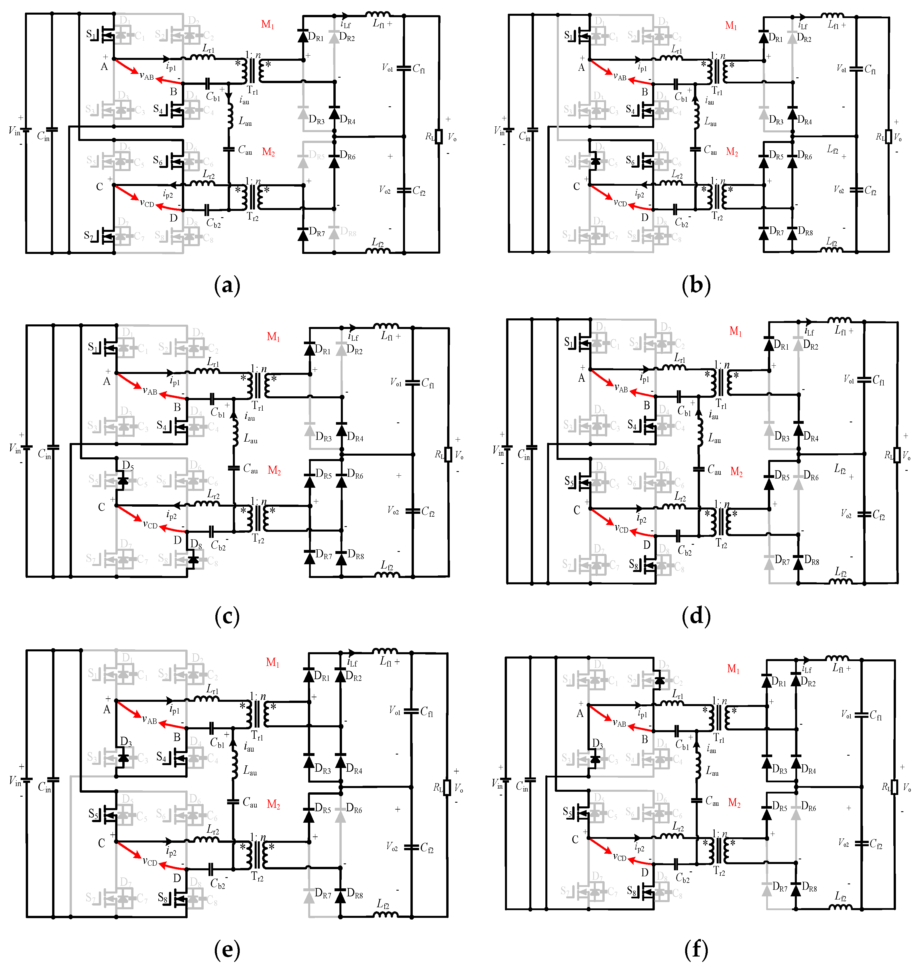
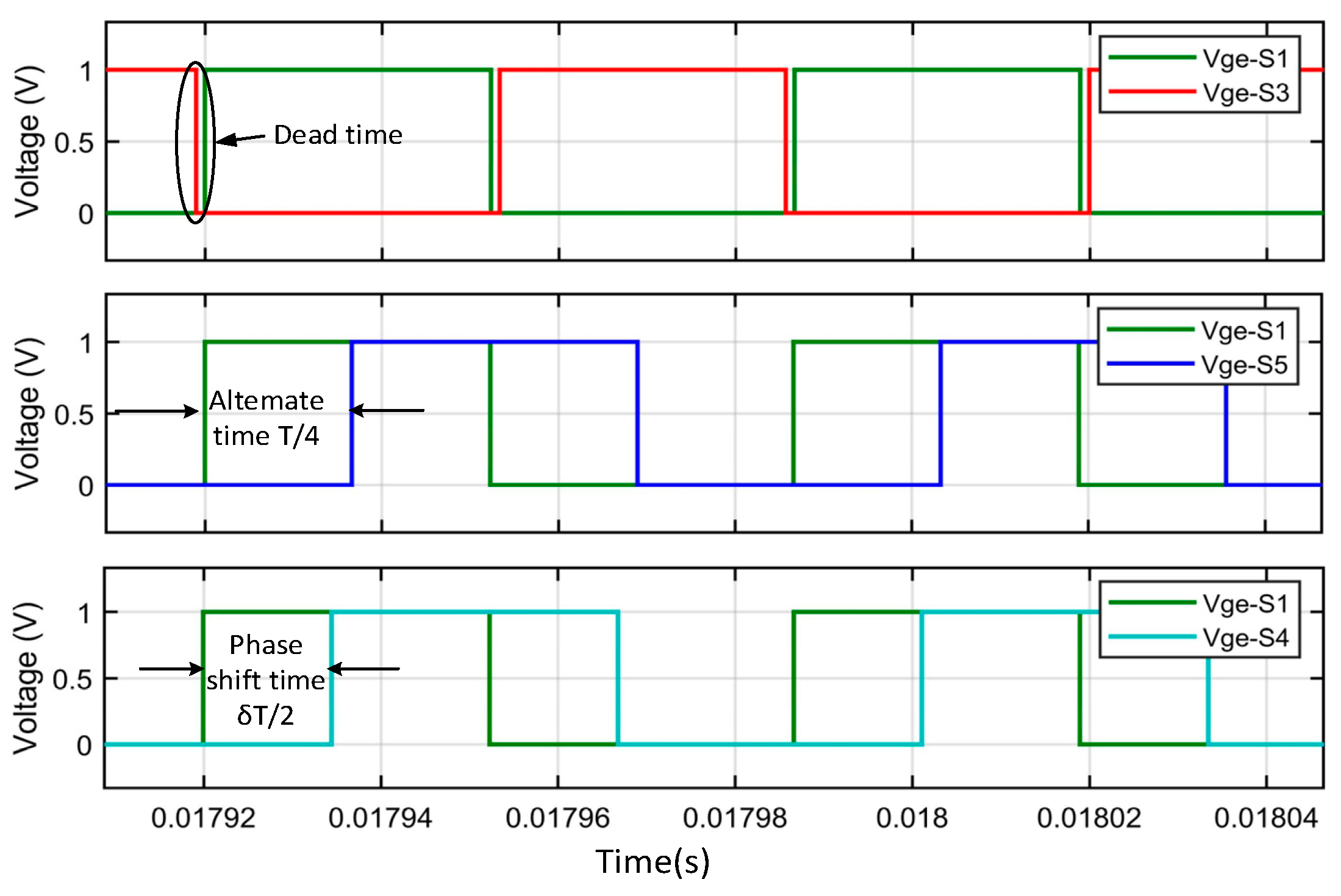
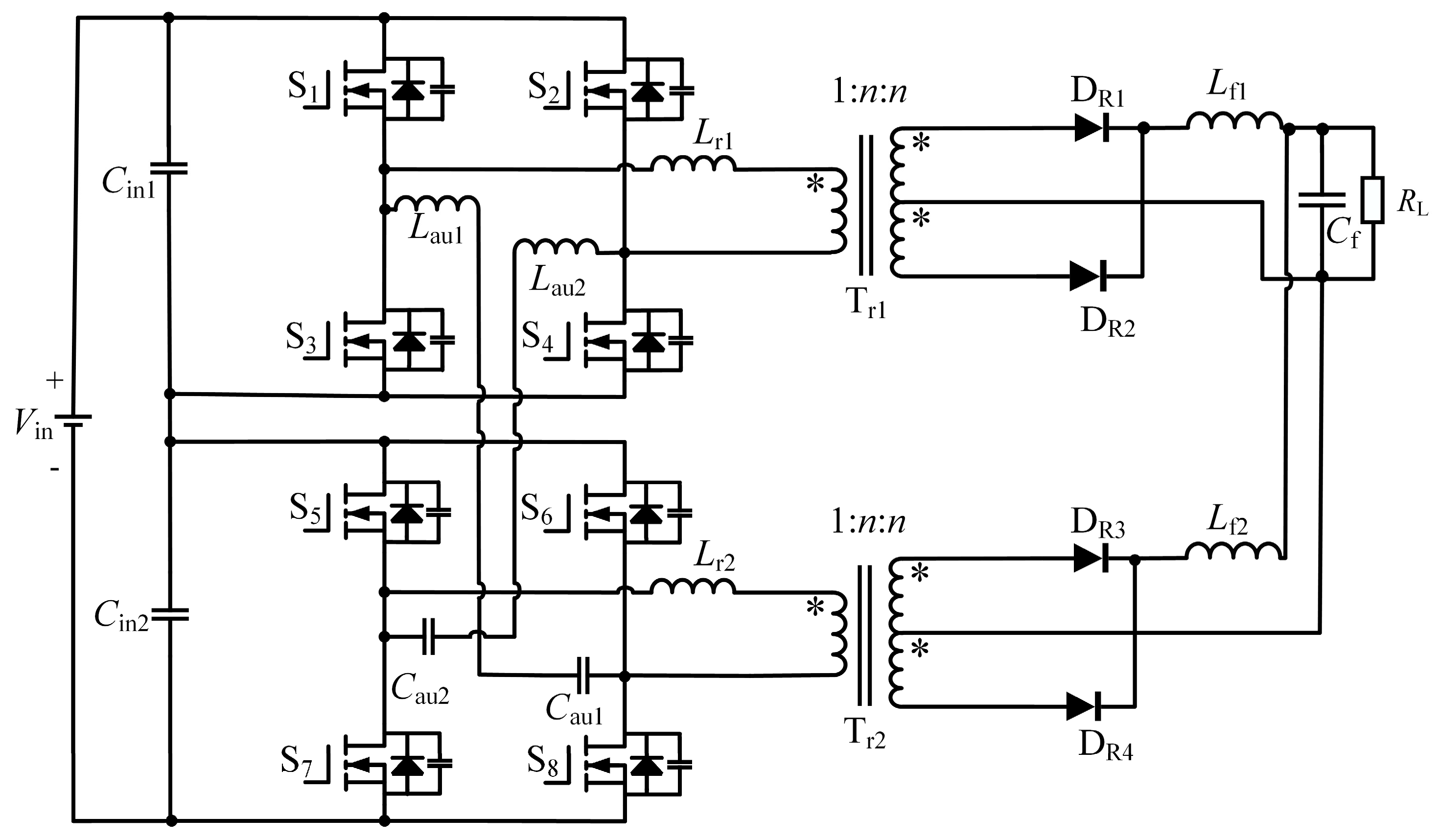
2. Working Principle of ZVS Series-Parallel PSFB Converter

The series-parallel PSFB converter is mostly used in medium and high-power applications, and its structure is shown in Figure 1. The differences in parasitic parameters between submodules for medium and high-power applications have a small impact on the performance of the converter, so the series-parallel PSFB converter submodules are often driven by interleaved synchronization as shown in Figure 2. In this driving mode, different sub-modules having the same duty cycle can not only realize the natural equalization of input current and output voltage between sub-modules, simplify the design of the control loop, and improve the reliability of the system, but also improve the input and output voltage and current ripple frequency and reduce the volume of input and output filtering components.
When the difference in parasitic parameters between series-parallel PSFB converter submodules is not considered, the input voltage of each submodule should be equal. To enable the lagging-leg to realize ZVS at light loads and higher input voltages, an LC passive auxiliary network can be connected between the midpoints of the lagging-legs of the series-parallel PSFB converter sub-modules in the interleaved driving mode.
Take the IPOS PSFB converter as an example to introduce the realization of the lagging-leg ZVS. The IPOS PSFB converter module is composed of two PSFB converter sub-modules connected in series via inputs in parallel with outputs. The main circuit of the IPOS PSFB converter after adding the LC auxiliary circuit is shown in Figure 2a. The addition of the auxiliary LC branch does not affect the working process of the IPOS PSFB converter, and the working principles of submodules M1 and M2 are the same as those of the conventional PSFB converter. The main waveforms of the IPOS PSFB converter are shown in Figure 2b after the addition of the auxiliary LC branch under interleaved driving.
In Figure 3a, S1-S4, S5-S8, DR1-DR4, and DR5-DR8 form the inverter H-bridge and rectifier H-bridge of the sub-modules M1 and M2, respectively. Lr1 and Lr2, Cb1 and Cb2, ip1 and ip2, and Vo1 and Vo2 are the resonance inductance (or transformer leakage inductance), the isolation capacitance, the primary-side currents, and the output voltages of the sub-modules M1 and M2, respectively. Vin and Cin are the input voltage and input capacitance of the IPOS PSFB converter. Lf1, Lf2, Cf1, Cf2, iLf1, iLf2, Vo1, Vo2, Vrect1, Vrect2, and RL are the filter inductors, filter capacitors, currents flowing through the filter inductors, output voltages, the rectified output voltages, and load resistors of the submodules M1 and M2, respectively. Lau, Cau, vEF, and iau are the inductance and capacitance of the auxiliary branch, the voltage across the auxiliary branch, and the current flowing through the auxiliary branch, respectively.
As shown in Figure 2b the duty cycles of all switch tubes S1-S8 are 50%, the phase angle differences of the diagonal switch tubes of submodules M1 and M2 are δ, and the driving signals of the corresponding switch tubes of submodule M2 lag behind the driving signals of the corresponding switch tubes of submodule M1 by 90° or Ts/4. Utilizing full-bridge diode rectification, the ripple frequency of Vo1 and Vo2 is two times the switching frequency. In addition, the ripple of the output voltage Vo is 4fs of the switching frequency because the submodule uses interleaved drive signals.
Due to the symmetry of the control method, the converter exists in 12 operating modes with positive and negative half-cycle symmetry during one switching cycle. The following section focuses on analyzing the operation of the ZVS IPOS PSFB converter during half a cycle of the [t0-t7] period.
Assumptions are made for analytical convenience as follows [28]:
  • The module works in a steady state;
  • Switching tubes S1-S8 and diodes DR1-DR8 are ideal devices;
  • Switch tubes S1-S8 parasitic capacitance C1 = C2 = --- = C8 = Cr;
  • Transformer Tr1, Tr2, inductors Lr1, Lr2, Lf1, Lf2, Lau and capacitors Cin, Cf1, Cf2, Cau are ideal devices, and Lr1 = Lr2, Lf1 = Lf2, and Cf1 = Cf2.
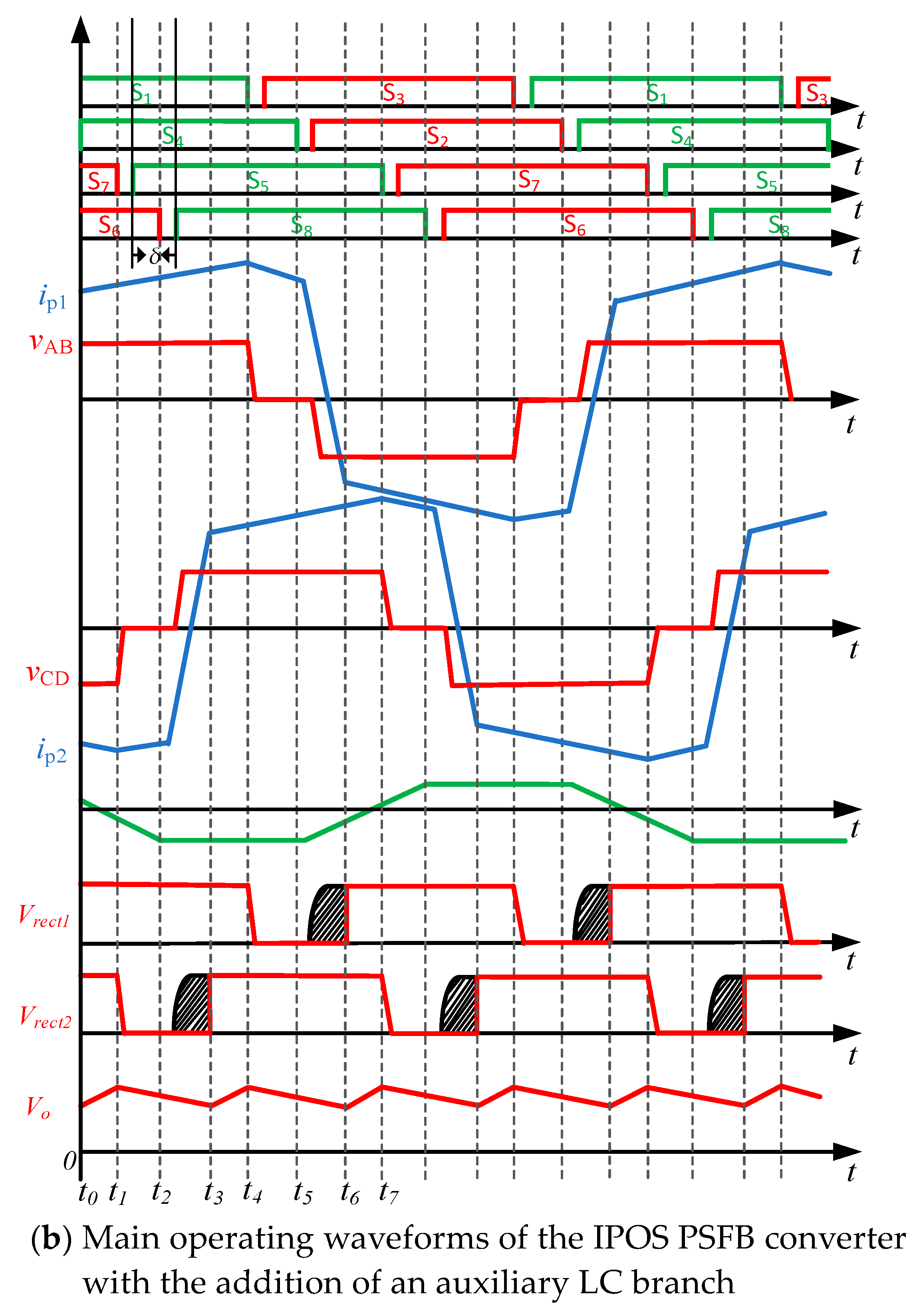
a.
Mode 0 [t0-t1]:
At the moment t0, the switching tubes S1 and S4 of the submodule M1 are on, the primary current ip1 increases to equal the converted value of the secondary current nilf1, and the diodes DR2 and DR3 are subjected to a counter voltage and turn off. The input power supply Vin charges the capacitor Cf1 through the submodule M1 while transferring energy to the load. The current iLf1 flowing through the filter inductor Lf1 increases linearly to the value of:
i L f 1 ( t ) = i L f 1 ( t 0 ) + n V i n V o 1 n 2 L r 1 + L f ( t t 0 )
The primary-side current of sub-module M1 equal to the converted value of the filter inductor current also increases linearly.
For sub-module M2, the primary side switching tubes S6 and S7 and the secondary side rectifier diodes DR6 and DR7 are in conduction. The primary energy is reflected to the secondary side by transformer Tr2, charging Cf2 and providing energy to the load. The current iLf2 flowing through the filter inductor Lf2 increases linearly with a value of:
i L f 2 ( t ) = i L f 2 ( t 0 ) + n V i n V o 2 n 2 L r 2 + L f ( t t 0 )
The primary-side current of submodule M2 is equal to -niLf2 linearly decreasing.
As the switching tubes S4 and S6 conduct, the voltage vEF across E and F is a lower positive and upper negative Vin, and the current iau flowing through Lau is:
i a u ( t ) = i a u ( t 0 ) V i n L a u ( t t 0 )
The iau decreases linearly and then increases inversely.
b.
Mode 1 [t1-t2]:
Turning off S7 at the moment of t1, the direction of the primary current ip2 of the sub-module M2 is unchanged due to the renewal of the primary resonant inductor Lr2. ip2 is transferred from S7 to the C5 and C7 branches, discharging C5 and charging C7. When the C5 discharge is over, D5 conducts and renews the current, after which switching tube S5 can be opened to realize ZVS when D5 or S5 conducts the primary and secondary voltages of transformer Tr2 are clamped to zero, and the rectifier diodes of sub-module M2 all conduct and renew the current. Since the switching state of switching tubes S1-S4 is unchanged, the operating state of submodule M1 is the same as mode 0. At this time, the filter capacitor Cf1 is in the charging state Cf2 is in the discharging state.
Switch tubes S4 and S6 are in conduction and iau increases inversely.
c.
Mode 2 [t2-t3]:
When S6 is turned off at t2, the direction of iau is unchanged due to the auxiliary inductor Lau, and Lau and Lr2 resonate with C6 and C8 together. The iau is transferred from S6 to C6 and C8 branches, discharging C8 and charging C6. When C8 is discharged, D8 conducts to continue current, and vEF is clamped to zero. Thereafter, switch S8 is turned on to realize ZVS. When C8 discharge is over, D8 conducts to continue the current, vEF is clamped to zero, iau is unchanged, and thereafter, turning on the switch S8 can realize ZVS. Due to the D8 continuing to conduct, the input voltage is all added to the resonant inductor Lr2, and the primary current ip2 of the sub-module M2 is first linearly reduced and then inversely increased with a value of:
i p 2 ( t ) = i p 2 ( t 2 ) + V i n L r 1 ( t t 2 )
The state of submodule M1 is the same as that of mode one. The sub-module M2′s secondary rectifier diode continues to conduct and renew the current.
d.
Mode 3 [t3-t4]:
At the moment, t3, the primary current ip2 of the submodule M2 is equal to the converted value of the secondary current nilf2, and the diodes DR5 and DR8 are subjected to a back-voltage and turned off. The input power Vin charges the capacitor Cf2 through the submodule M2 and transfers energy to the load. Since the state of the inverter bridge arm switching tube of submodule M1 remains unchanged, the operating state of submodule M1 is the same as that of mode two. The current iLf2 flowing through the filter inductor Lf2 is:
i L f 2 ( t ) = i L f 2 ( t 3 ) n V i n V o 2 n 2 L r 2 + L f ( t t 3 )
The filter inductor current increases linearly, and the primary side current ip2 of sub-module M2, which is equal to the converted value of the filter inductor current, also increases linearly.
Switch tubes S4 and S8 conduct, the voltage vEF across E and F is clamped to zero, and iau is essentially unchanged.
e.
Mode 4 [t4-t5]:
Turning off S1 at the moment of t4, the direction of the primary current ip1 of the submodule M1 remains unchanged due to the renewal of the primary resonant inductor Lr1. The ip1 is transferred from S1 to the C1 and C3 branches, discharging C3 and charging C1. When the end of C3 discharge, D3 conduction renewal, and turning on the switch S1 can realize ZVS. Due to the D3 conduction renewal, transformer Tr1 primary and secondary side voltage is clamped to zero, DR1-DR4 all conduction renewal. Submodule M2 operates in the same state as mode 3.
f.
Mode 5 [t5-t6]:
When S4 is turned off at t5, the direction of iau is unchanged due to the continuity of the auxiliary inductor Lau, Lau, and Lr1 resonate together with C2 and C4, and iau is transferred from S4 to the C2 and C4 branches, discharging C2 and charging C4. When C2 discharge is over, D2 conducts to renew the current, after which switch S2 can be turned on to realize the ZVS. Due to the D2 renewed conduction, the input voltage is all added to the resonant inductor Lr1, and the primary current ip1 of the sub-module M1 first decreases linearly, and then increases inversely with a value of:
i p 1 ( t ) = i p 1 ( t 5 ) V i n L r 1 ( t t 5 )
Since the switching tube state of submodule M2 is unchanged, the operating state of M2 is the same as that of mode 4.
Since the switching tubes S2 and S8 are on, the voltage vEF across E and F is Vin which is positive up and negative down, and the current iau flowing through Lau is:
i a u ( t ) = i a u ( t 5 ) V i n L a u ( t t 5 )
The iau decreases linearly.
At the moment, t6, the primary side current ip1 of the submodule M1 is equal to the converted value of the filter inductor current, niLf1, and the converter enters into the next half-cycle, which works similarly to that of the first half-cycle.
The equivalent circuit of the ZVS IPOS PSFB converter operating mode is shown in Figure 3.
From the operating principle of the ZVS IPOS PSFB converter, it is clear that when the input voltage is determined, the energy of the auxiliary inductor is only related to the interleaving time between submodules and the size of the auxiliary inductor but not to the state of the load and the size of the resonant inductor. For the series-parallel PSFB converter under interleaved control, regardless of whether the input ports of the sub-modules are connected in parallel or series, the energy balance of the auxiliary LC branch in one cycle can be guaranteed by ensuring that the input voltage of each sub-module is of equal magnitude, and thus the strategy applies to all four combining forms of the series-parallel PSFB converter.

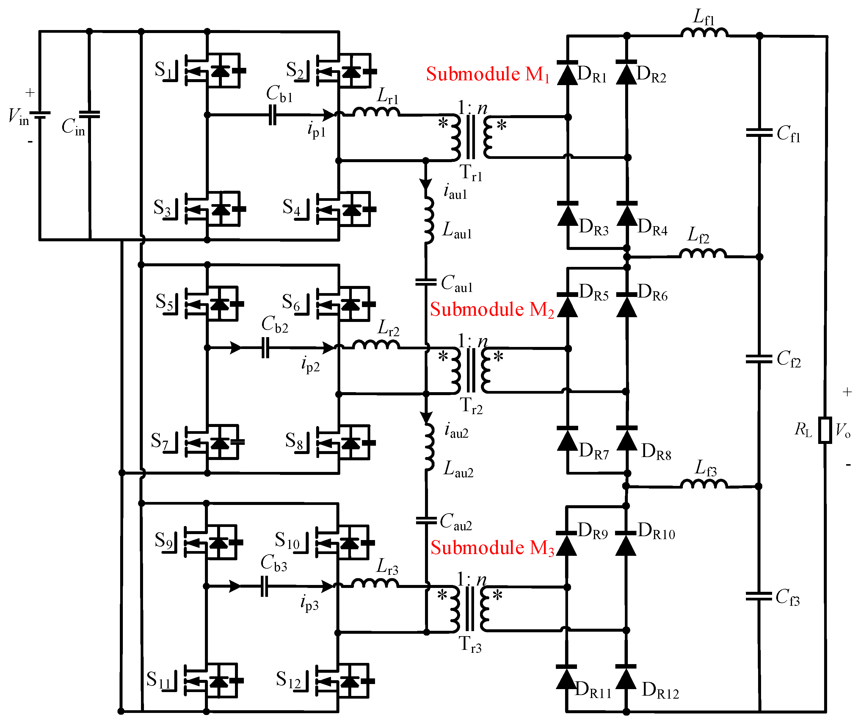
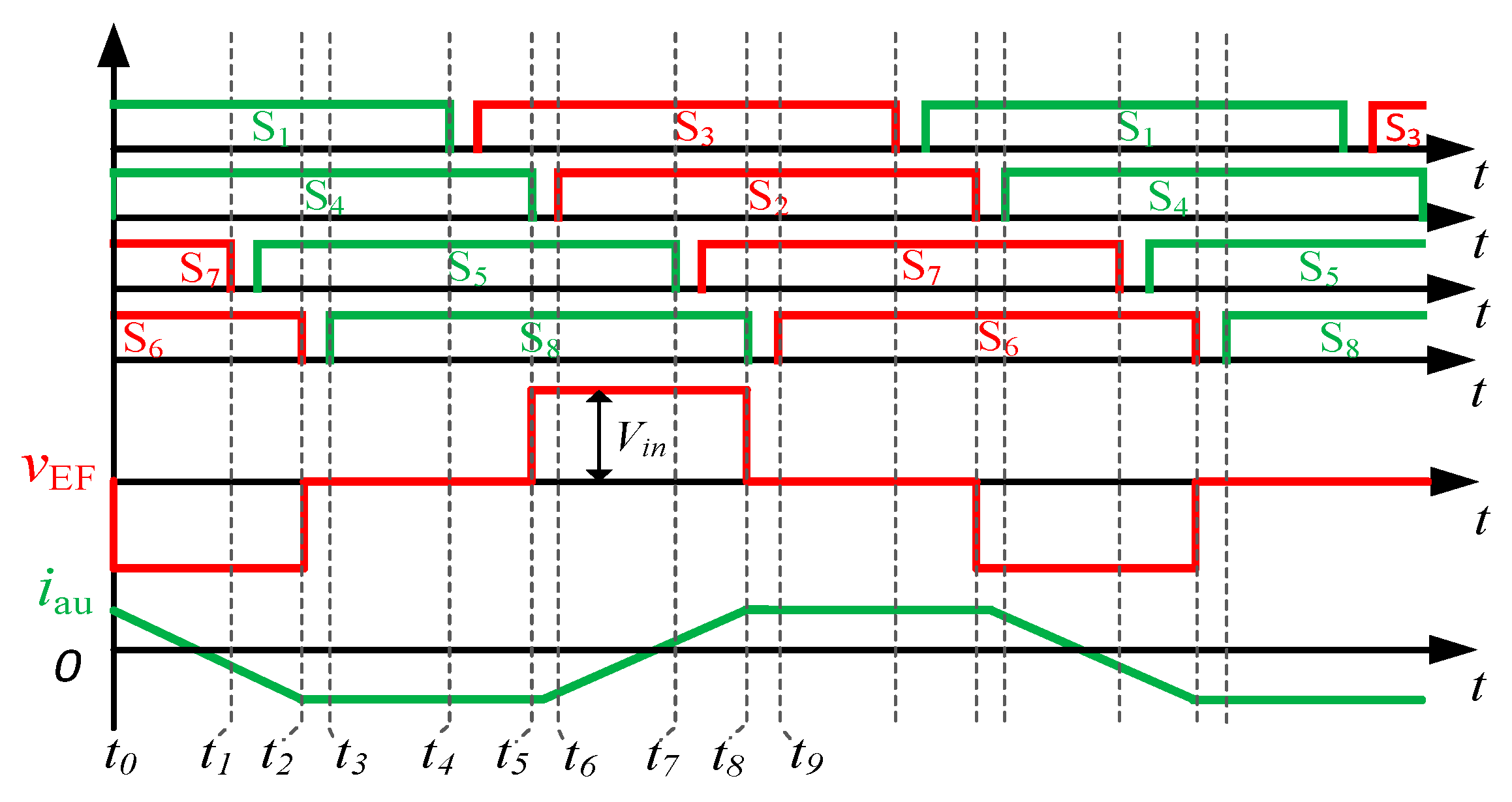
3. Series-Parallel PSFB Converter ZVS Condition and N-Bridge Extension

3.1. Series-Parallel PSFB Converter ZVS Condition

The primary resonant inductor makes the rising and falling edges of the primary current of the PSFB converter have a finite slope causing the loss of the secondary duty cycle. The expression for the output voltage Vo of a conventional PSFB converter can be written as:
V o = n V i n D e f f
where Deff is the effective duty cycle of the secondary side.
As illustrated in Figure 2b, the leading-leg switching tubes of each submodule are turned on or off when the primary-side current reaches its maximum value. At this time, the equivalent value of the filter inductor Lf at the primary side is involved in the resonance of the switching tube section capacitance together with the primary side resonant inductor to complete the charging and discharging of the upper and lower bridge arm capacitors. Before turning on, the leading-leg switching tube allows its anti-parallel diode natural conduction. Due to the conduction of the switching tube anti-parallel diode, the output voltage of the inverter H-bridge is clamped to zero, and the magnitude of the primary current is almost unchanged, which ensures that the switching tube anti-parallel diode is in the conduction state when the drive signal of the leading-leg arrives, and thus the ZVS of the switching tube of the leading-leg can be guaranteed. Therefore, the ZVS of the leading-leg can be realized by the resonant inductance of the circuit or the transformer leakage inductance without the need for additional auxiliary circuits.
To realize the ZVS of the switching tube of the leading-leg, there must be enough energy to draw out the charge of the shunt capacitors at both ends of the switching tube that is about to turn on, and to complete the charging of the shunt capacitors at both ends of the switching tube that is about to turn off in the same bridge arm. To realize the ZVS of the leading-leg switching tube, it is necessary to satisfy:
1 2 ( L r + L f ) I p 2 C i V i n 2
where Ip is the peak value of the current flowing through the primary resonant inductor and its value is:
I p = V o i T s ( 1 D e f f ) + 4 L f I o 4 L f
As demonstrated in Figure 2b, the primary side current Ip is almost constant during the switching process of the leading-leg. Since the filter inductor is generally large, the energy stored in the original resonant inductor and the filter inductor can help the leading-leg to realize ZVS under the condition that the dead time meets the requirement, and thus, the leading-leg can realize ZVS over a wide load range.
Each sub-module of the series-parallel PSFB converter realizes the ZVS of the lagging-leg in the same way as the conventional PSFB converter. Therefore, the series-parallel PSFB converter is mainly concerned with the ZVS of the lagging-leg.
Unlike the ZVS of the leading-leg, when the lagging-leg switching tube is turned off, the primary and secondary sides of the transformer are uncoupled, and only the primary resonant inductor resonates with the junction capacitance of the lagging-leg switching tube. Therefore, to realize the ZVS of the lagging-leg, there must be enough energy to pump away the charge of the shunt capacitance at both ends of the switching tube that will be turned on and complete the charging of the shunt capacitance at both ends of the switching tube that will be turned off in the same bridge arm. However, the primary resonant inductor is generally very small, and when the load is light, the energy of the primary resonant inductor is not enough to realize the charging and discharging of the junction capacitors of the switching tubes in the lagging-leg. At the same time, when the input voltage of the series-parallel PSFB converter is high and the resonant inductance is small, the primary current of the transformer drops to zero before the driving signal of the switching tube of the lagging-leg arrives, and the anti-parallel diode of the switching tube cuts off so that the lagging-leg is unable to realize ZVS.
The auxiliary LC branch can not only realize the charging and discharging of the junction capacitance of the lagging-leg switching tube together with the resonant inductor when the lagging-leg switching tube is off but also renew the current through the anti-parallel diode after the anti-parallel diode of the lagging-leg switching tube conducts, which is a very good solution to the two problems that it is difficult for the lagging-leg to realize the ZVS in light loads and when the input voltage is high. Thus, ZVS of the lagging-leg can be realized over the full load range. According to the analysis of the operating principle of the IPOS PSFB converter with LC auxiliary branch in Section 2, the voltage and current waveforms of the auxiliary LC branch can be shown in Figure 4.
The maximum value of the auxiliary inductor current, Iaumax, can be seen in Figure 4.
I a u m a x = V i n T s 8 L a u
Iaumax is only related to the staggering time between submodules, the input voltage, and the size of the auxiliary inductor. To realize the ZVS of the lagging-leg of a series-parallel PSFB converter, it is only necessary to ensure the following three items:
(1) The energy of the auxiliary inductor should be greater than the minimum energy required to complete charging and discharging of the junction capacitance of the switching tube i.e., Lau should be satisfied
L a u T s 2 128 C j
(2) The drain-source pole parasitic capacitance of the lagging-leg switching tube needs to finish charging and discharging during the dead time, and the auxiliary circuit current cannot be reversed during the dead time, both to ensure
16 C j L a u T s t d , l a g g i n g T s 8
(3) To ensure that there is no DC bias current in the auxiliary circuit, an isolation capacitor Cau is connected in series with the auxiliary circuit to ensure that the resonant frequency of the auxiliary circuit is less than 1/5 of the switching frequency.
C a u 1 ( 2 π 5 T s ) 2 L a u
When the difference in parasitic parameters between the sub-modules of the series-parallel PSFB converter is not considered, the input voltage of each sub-module should be equal. Therefore, the series-parallel PSFB converter with the addition of the auxiliary circuit LC has the same operating principle as the main circuit and the same operating state of the auxiliary circuit as the IPOS PSFB converter. Therefore, this strategy is applicable in all four series-parallel PSFB converters under interleaved synchronous drive.
For a series-parallel PSFB converter composed of two PSFB converter submodules, due to the staggered 90° driving method between the submodules, it can be seen from Figure 4 that the current iau flowing through the LC branch is symmetrical about the zero point of the current, and the average value of the current flowing through the LC branch in each switching cycle in the ideal case is zero. From the working process of the LC branch in Section 2, it can be seen that in one switching cycle, the flow path of current iau does not pass through the transformer’s primary edge. Therefore, the energy stored in the LC branch is not reflected to the secondary side via the transformer but is all fed back to the input power supply. Thus, the LC branch does not transfer energy to the secondary edge nor does it exacerbate the parasitic oscillations of the secondary diode. For the primary side of the transformer, iau only flows through the lagging-leg and flows through the same switching tube or anti-parallel diode as the primary side of the transformer, so this does not exacerbate the voltage spikes of the switching tube. In addition to this, the auxiliary inductor should be designed to minimize the current in the LC network by taking into account the dead time and the input voltage.
To further analyze the efficiency improvement of IPOS phase-shifted full-bridge converter lagging-leg realizing ZVS versus not realizing ZVS, at a rated power of 100 kW, a loss analysis is conducted under various working conditions after determining the main circuit parameters. The losses of each component in the module are shown in Table 1, and the efficiency and efficiency difference curves of the lagging-leg realizing ZVS and the non-realized ZVS module at input voltages of 205 V-320 V are shown in Figure 5. Figure 5 shows that the higher the input voltage, the lower the efficiency because of the increased switching losses in the active switch and iron losses in the transformer. It can also be seen that the percentage difference in efficiency between the lagging-leg achieving zero-voltage turn-on and not achieving zero-voltage turn-on increases gradually as the input voltage increases the percentage efficiency difference is 1.09 when the input voltage is 320 V. That is to say, realizing zero voltage turn-on of the lagging-leg improves the efficiency more when the input voltage is higher.

3.2. Implementation of Lagging-Leg ZVS for N-Bridge ZVS Series-Parallel PSFB Converter

N PSFB converter submodules are usually combined in series-parallel to meet higher power demands. The concept of lagging-leg ZVS for a series-parallel PSFB converter realized by a dual-bridge LC auxiliary branch can be extended to a series-parallel PSFB converter composed of N submodules. Figure 6 shows a circuit topology consisting of three PSFB converter submodules passing through IPOS. To realize the ZVS of the lagging-leg switching tubes of each PSFB converter submodule, the topology adds two auxiliary LC branches with identical parameters at the midpoints of the lagging-legs of the neighboring submodules.
In a series-parallel PSFB converter consisting of n PSFB converter submodules, the interleaving angle of the corresponding switching tubes between two neighboring submodules should be π/n. So, in a series-parallel PSFB converter consisting of three PSFB converter submodules, the interleaving angle between two neighboring modules should be π/3.
From Figure 4, it can be seen that the auxiliary inductor current varies linearly throughout the staggered angle and is renewed when the corresponding switching tubes of the lagging-legs turn on at the same time between neighboring submodules. For a series-parallel PSFB converter consisting of n submodules, the maximum value of the auxiliary inductor current Iaumax,n is
I a u m a x , n = V i n T s 4 n L a u
When the size of the auxiliary inductor is constant, it can be seen from (15) that the maximum value of the auxiliary inductor current is smaller as the number of series-parallel PSFB converter submodules increases. This is not difficult to understand because the auxiliary inductor only obtains energy from the input power supply during the interleaving time, and the interleaving angle becomes smaller as the number of series-parallel PSFB converter sub-modules increases. Therefore, to be able to realize the ZVS of the lagging-leg, the auxiliary inductance should be smaller as the number of series-parallel PSFB converter sub-modules increases. For a series-parallel PSFB converter consisting of n PSFB converter submodules, the size of the auxiliary inductance Lau should be satisfied
L a u T s 2 32 n 2 C j
From Figure 6 and the realization of the lagging-leg ZVS with the addition of the auxiliary circuit, it can be seen that for a series-parallel combined converter consisting of N PSFB converter sub-modules, the current flowing through the lagging-leg of the intermediate module is twice as much as that of the first sub-module and the Nth sub-module when N ≥ 3, which leads to a higher conduction loss.
For high-power converter applications, the number of submodules of the series-parallel converter must be determined to balance component stress, efficiency, cost, and power density. After performing this analysis and determining the number of submodules of the series-parallel combined PSFB converter, the optimal combination of series-parallel PSFB converter topologies can be selected. The double bridge topology provides the best cost and performance tradeoffs and is, therefore, more widely used.

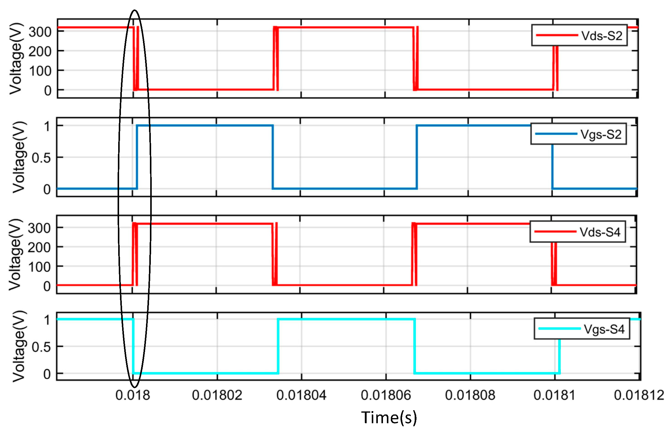
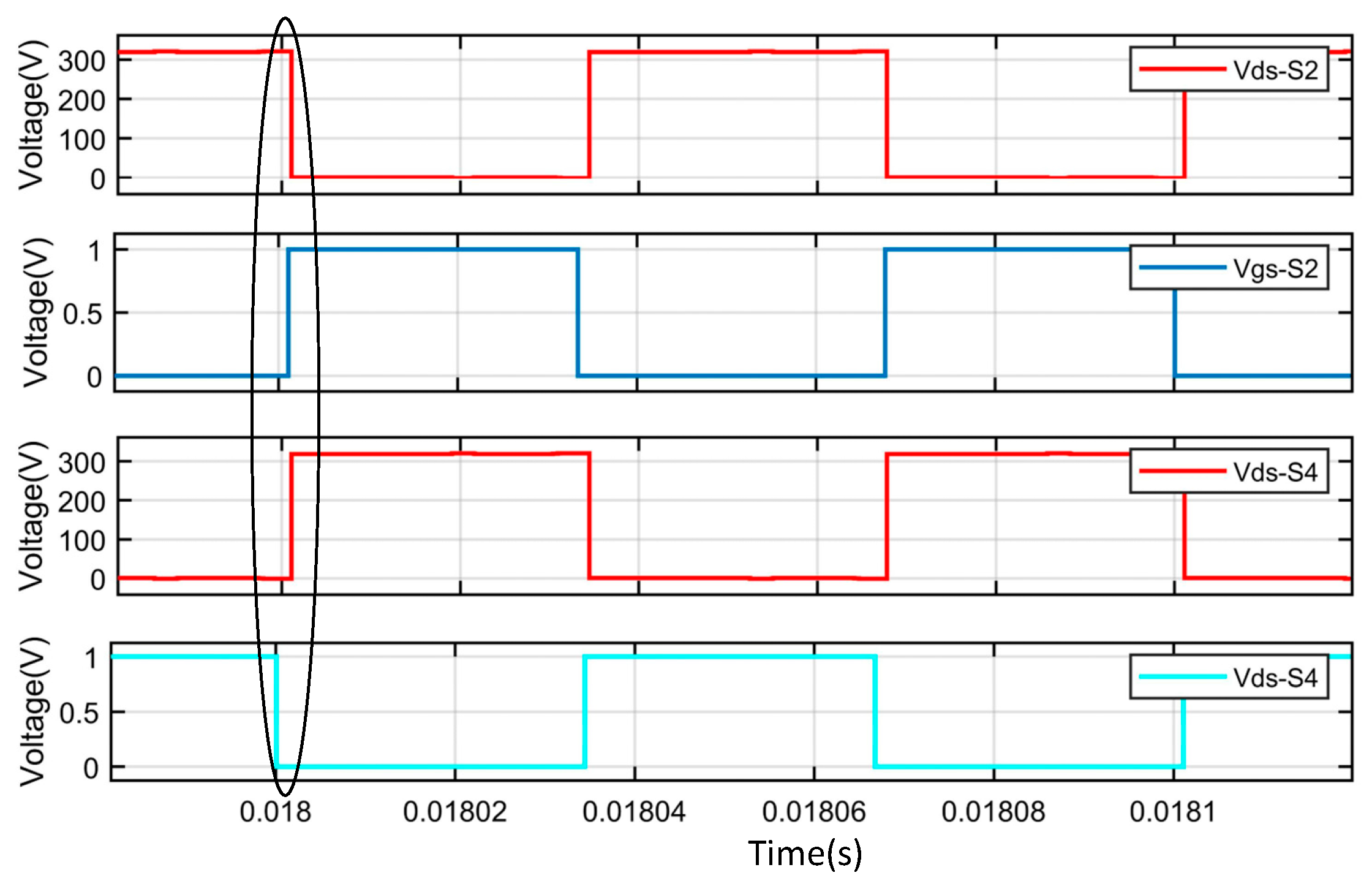
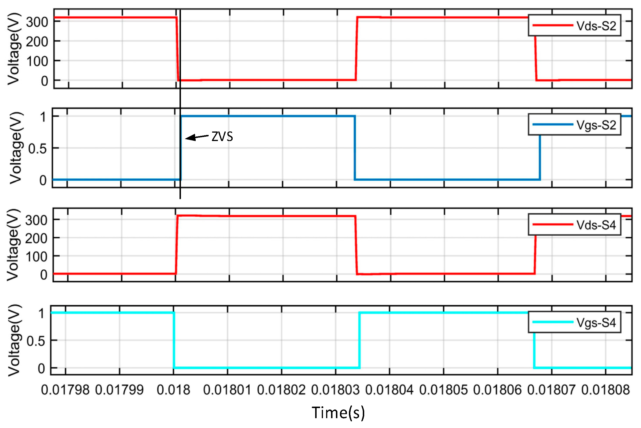
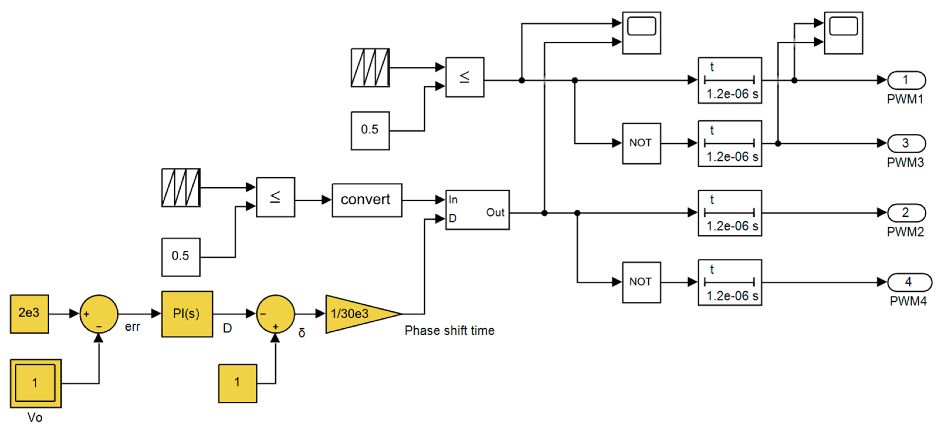
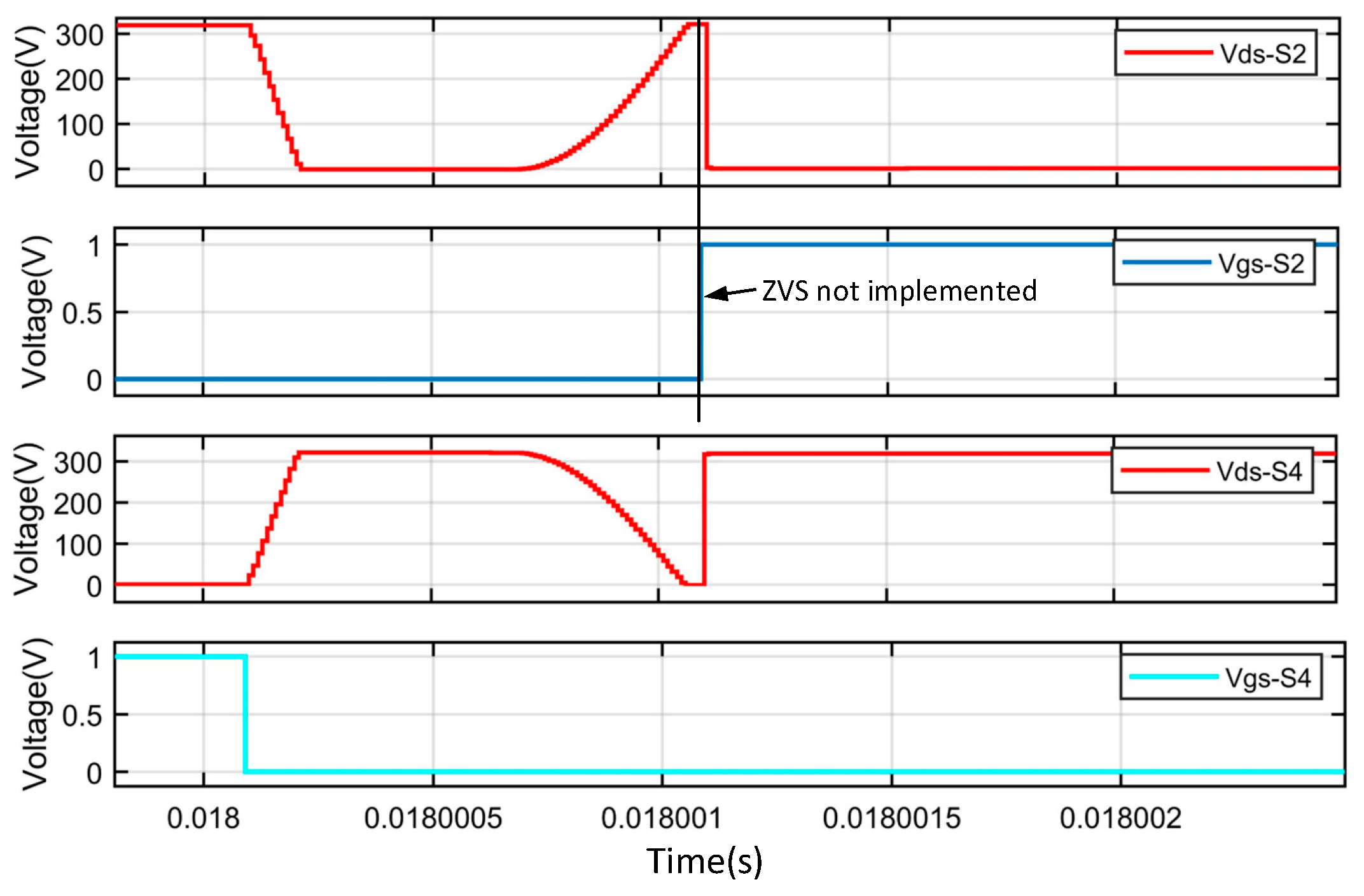
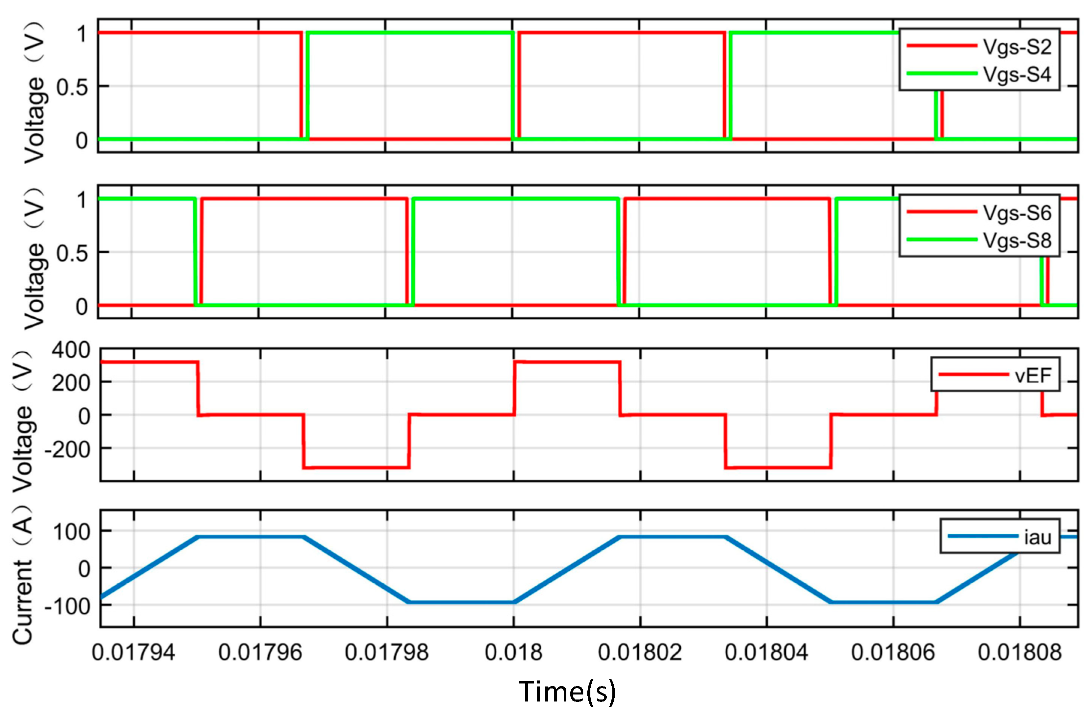
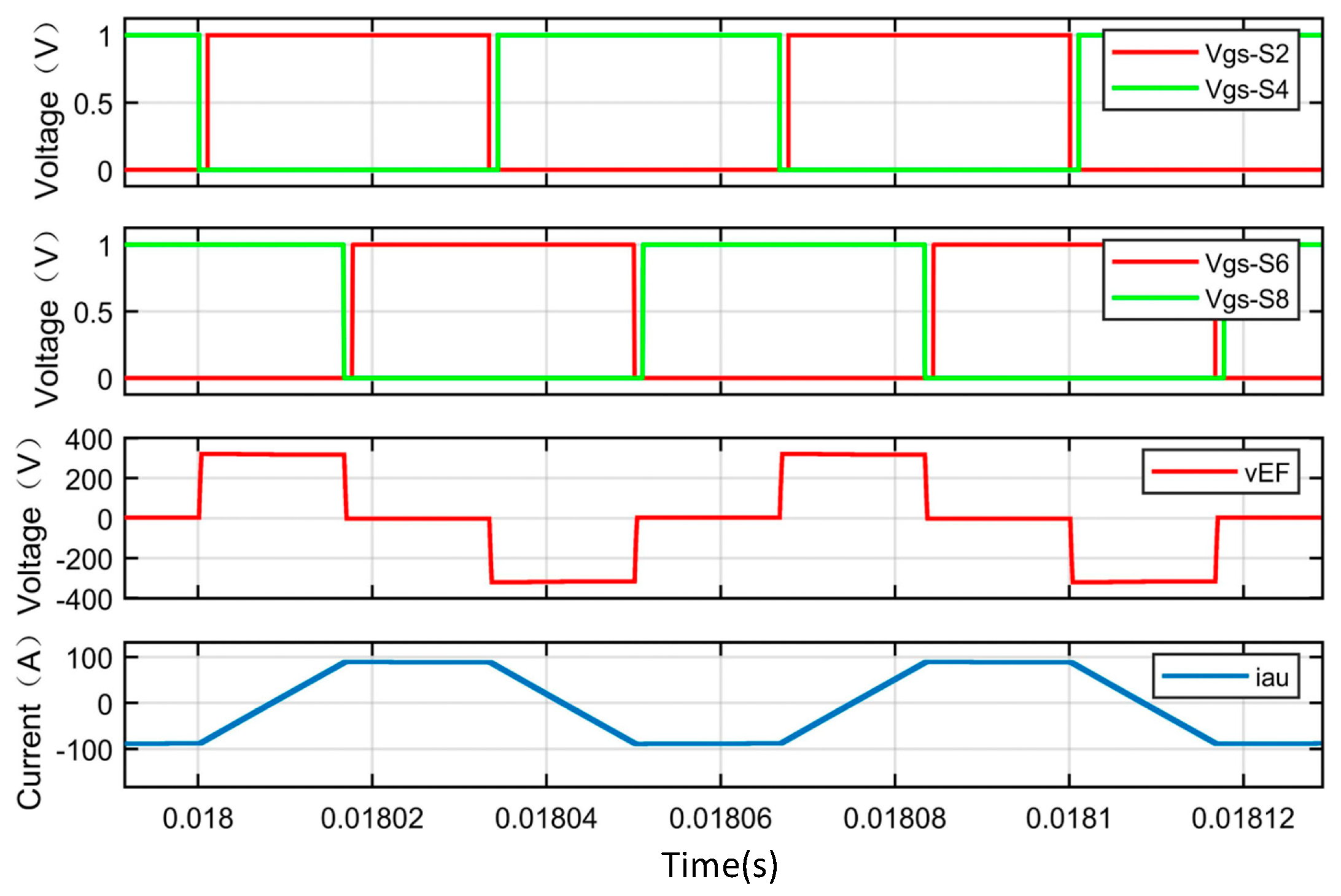
4. Simulation Results and Discussion

To validate the series-parallel PSFB converter lagging-leg ZVS strategy, a two-bridge 100 kW ZVS IPOS PSFB converter is modeled by the Matlab/Simulink simulator as shown in Figure 7 and Figure 8, and its model parameters are shown in Table 2. In the simulation, the controller is controlled by a single voltage loop, and a Proportional Integral (PI) controller is used to balance the output voltage. The control parameters of the PI controller are Kp = 0.0001 and Ki = 0.3.

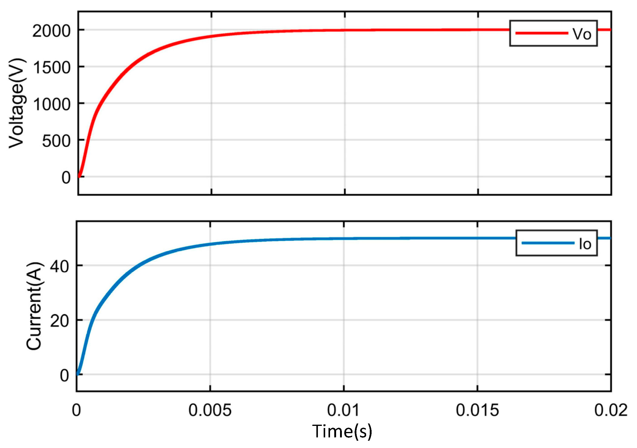
4.1. Simulation Results under Rated Load for an Input Voltage of 320 V

To analyze the reason for the difficulty in achieving ZVS for the lagging-leg at high input voltage and rated load, the steady-state analysis of the ZVS IPOS PSFB converter is implemented when the input voltage is 320 V at a rated load with 40 Ω load resistance. The driving voltage waveforms of the module are given in Figure 9, from top to bottom, the driving signals of the switch tubes S1 and S3 above and below the same bridge arm of the module, the driving signals of the corresponding switch tubes S1 and S5 between the sub-modules, and the driving signals of the diagonal switch tubes S1 and S4 under the rated power at the input voltage of 320 V. The output voltage and current waveforms are shown in Figure 10 with Vo = 2000 V and Io = 50 A at steady state.
Figure 11 gives the realization of ZVS of the submodule M1 lagging-leg switch tubes S2 and S4 before the addition of the auxiliary LC branch at an input voltage of 320 V and a resonant inductance of 1μH Figure 12 shows a partial enlargement of Figure 11. From Figure 12, it can be seen that the drain and source voltages Vds-S2 of the switching tube S2 decrease to zero and then return to the input voltage before the arrival of the gate and source signals Vgs-S2 and the ZVS of the lagging bridge-arm switching tube is not realized. The reason for not realizing ZVS for the lagging-leg is precisely the fact that the transformer primary current drops to zero before the drive signal for the switching tube of the lagging-leg arrives causing the switching tube’s anti-parallel diode to cut off.
Figure 13 shows the voltage vEF, current iau of the auxiliary branch, and the driving voltage of the lagging bridge switch tubes of submodules M1 and M2 after adding the auxiliary inductor, and the maximum value of iau is 88 A when Vin = 320 V and Lau = 30 mH. The waveforms of drain-source voltage and gate-source voltage of the lagging bridge switch tubes S2 and S4, after adding the auxiliary inductor under the same working condition, are shown in Figure 14. It can be seen that the drain-source voltage has dropped to zero before the arrival of the drive signal of S2, thus realizing the ZVS of the craggy switching tube afterward.

4.2. Simulation Results under Light Load for an Input Voltage of 320 V

To analyze the reason for the difficulty in achieving ZVS in lagging-leg under light load, and comparison of achieving ZVS in lagging-leg with LC auxiliary branch under light load and rated load, the same simulation is completed at an input voltage of 320 V and 5 kW load. Figure 15 shows the waveforms of the drive signals of switch tubes S1 and S3 above and below the same bridge arm at a load of 5 kW, the drive signals of the corresponding switch tubes S1 and S5 between the submodules, and the drive signals of the diagonal switch tubes S1 and S4 at a rated power with an input voltage of 320 V, while the other conditions remain unchanged. Under the same input and output voltages, the phase angle difference between switch tubes S1 and S4 in Figure 15 is significantly larger than that in Figure 9, which is because the primary current of the transformer is significantly reduced under light load, thus reducing the loss of the primary duty cycle. The output voltage and current waveforms are shown in Figure 16, with Vo = 2000 V and Io = 2.5 A at steady state.
Figure 17 shows the realization of ZVS by the submodule M1 lagging-leg switch tubes S2 and S4 before the addition of the auxiliary LC branch at an input voltage of 320 V and a resonant inductance of 1μH under light load conditions. Figure 18 shows a partial enlargement of Figure 17 from Figure 18, it can be seen that the drain and source voltages Vds-S2 of switch S2 maintain the input voltage unchanged until the arrival of the gate and source signals Vgs-S2 and the ZVS of the lagging bridge switching tubes is not realized. The reason why the lagging-leg does not realize the ZVS under the light-load condition is that the energy of the resonant inductor is not enough to realize the charging and discharging of the junction capacitance of the switching tubes of the lagging-leg.
The voltage and current waveforms of the submodules M1 and M2 lagging-leg switching tubes and auxiliary branches are shown in Figure 19. From Figure 13 and Figure 19 it can be seen that the voltage vEF and current iau of the auxiliary branch under light load are the same as those under rated load, which also verifies that vEF and iau are only related to the input voltage, interleaving time, and the size of the auxiliary inductance, but not the size of the load. As can be seen from Figure 20, the lagging bridge-arm switching tube also realizes ZVS after adding the auxiliary LC branch under light load conditions.

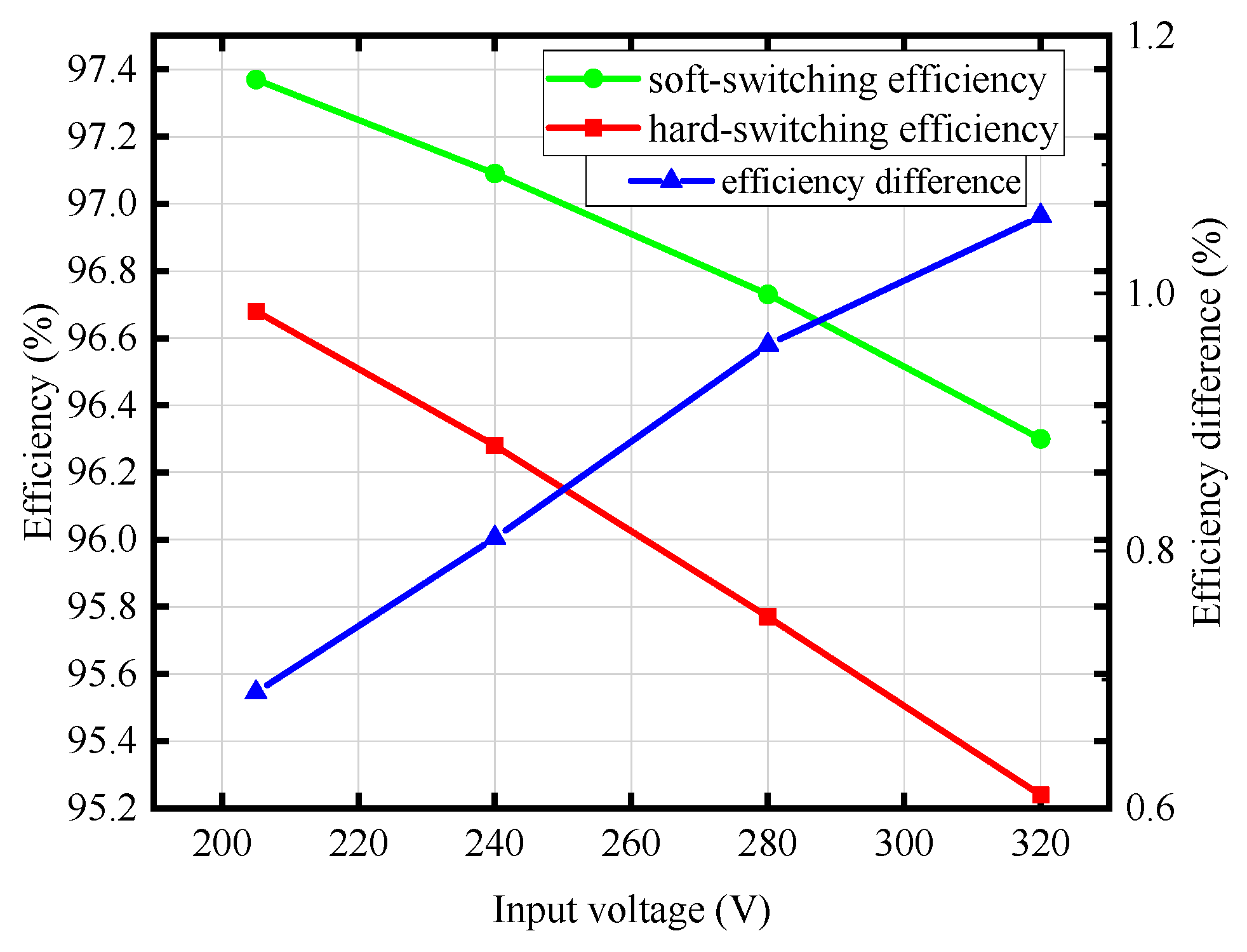
4.3. Comparative Study

Figure 21 gives the ISOP PSFB converter proposed in the literature [25] that possesses auxiliary LC networks to widen the ZVS range. The converter realizes the ZVS of all switching tubes by adding two auxiliary LC networks at the midpoints of the leading and lagging bridge arms of the neighboring submodules, and the scheme cleverly uses the interleaving of drive signals between submodules to make the energy of the auxiliary inductors vary with the duty cycle of the primary side.
Compared with the scheme presented in this paper, the drive signals of sub-modules M1 and M2 in this scheme are interleaved by 180 degrees, which increases the peak-to-peak input and output capacitance ripple. The series-parallel PSFB converter is mostly used in high-power scenarios, where the leading-legs can rely on the energy of the resonant inductor to realize the ZVS, and the two sets of LC auxiliary networks not only increase the circulating current loss but also reduce the power density of the module.

5. Conclusions

Aiming at the problem that the lagging-leg of a series-parallel PSFB converter is difficult to realize ZVS in high-power applications, the paper analyzes the reasons why the lagging-leg of a series-parallel PSFB converter is difficult to realize ZVS in light and heavy loads, and then proposes a strategy of adding auxiliary LC branch to realize ZVS in the full-load range with the interleaved control. This strategy achieves the ZVS of the lagging-leg independent of the states of load and input voltage by utilizing the interleaving of drive signals between submodules to energize the auxiliary LC branch. The following conclusions can be drawn from the analysis of the 100 kW simulation model under light and heavy loads:
(1) The auxiliary LC branch can be connected in parallel with the resonant inductor to realize the charging and discharging of the junction capacitance of the lagging-leg switching tube when the lagging-leg switching tube is turned off. This solves the problem that the energy of the resonant inductor is not enough to charge and discharge the junction capacitor of the lagging bridge switch under light loads.
(2) When the bridge arm switching tube is turned off afterward, the auxiliary LC branch is connected in parallel with the resonant inductor, and the ZVS of the lagging-leg switching tube can be realized during the dead time of the lagging-leg as long as the current of the auxiliary LC branch is not zero and is not reversed. It solves the case where the resonant inductor is too small at high input voltage causing the transformer primary current to drop to zero before the end of the dead time and causing the anti-parallel diode to cut off before the arrival of the drive signal of the lagging-leg.
(3) Compared with the traditional ZVS realization strategy for PSFB converter lagging bridge-arm switching tubes, for the two-bridge series-parallel PSFB converter this strategy only requires a set of passive LC auxiliary branches to realize the ZVS of the lagging bridge-arm four switching tubes, which significantly improves the reliability and power density of the system.
The implementation strategy proposed in this paper to realize the ZVS of the lagging-leg of a series-parallel PSFB converter can realize the ZVS of the lagging-leg in the full load range. However, the addition of an LC auxiliary branch at the mid-point of the lagging-leg increases the circulating current loss. Therefore, a switching device with a larger current stress should be selected for practical applications.

Author Contributions

Conceptualization, Y.W., F.S. and J.C.; methodology, Y.W., F.S. and J.C.; formal analysis, J.C. and H.C.; investigation, Y.W., F.S. and J.C.; resources, J.C. and H.C.; data curation, J.C.; writing—original draft preparation, F.S.; writing—review and editing, Y.W., F.S., J.C., H.C. and S.G.; funding acquisition, J.C. All authors have read and agreed to the published version of the manuscript.

Funding

This research was funded by the National Natural Science Foundation of China, grant number 51607060; Key Research and Development Projects of Hubei Province (2022BID012).

Data Availability Statement

The data in this article are available to all readers; please contact the corresponding author for access.

Conflicts of Interest

The authors declare no conflict of interest.

References

  1. Kasper, M.; Bortis, D.; Kolar, J.W. Classification and comparative evaluation of PV panel-integrated DC–DC converter concepts. IEEE Trans. Power Electron. 2014, 29, 2511–2526. [Google Scholar] [CrossRef]
  2. Lu, Y.; Sun, K.; Wu, H.; Dong, X.; Xing, Y. A three-port converter based distributed DC grid connected PV system with autonomous output voltage sharing control. IEEE Trans. Power Electron. 2019, 34, 325–339. [Google Scholar] [CrossRef]
  3. Chen, J.; Liu, C.; Liu, H.; Li, G. Zero-voltage switching full-bridge converter with reduced filter requirement and wide ZVS range for variable output application. IEEE Trans. Ind. Electron. 2022, 69, 6805–6816. [Google Scholar] [CrossRef]
  4. Shi, Y.; Feng, L.; Li, Q.; Kang, J. High power ZVZCS phase shift full bridge DC–DC converter with high current reset ability and no extra electrical stress. IEEE Trans. Ind. Electron. 2022, 69, 12688–12697. [Google Scholar] [CrossRef]
  5. Kanamarlapudi, V.R.K.; Wang, B.; Kandasamy, N.K.; So, P.L. A New ZVS Full-Bridge DC–DC Converter for Battery Charging With Reduced Losses Over Full-Load Range. IEEE Trans. Ind. Appl. 2018, 54, 571–579. [Google Scholar] [CrossRef]
  6. Liu, G.; Wang, B.; Liu, F.; Wang, X.; Guan, Y.; Wang, W.; Wang, Y.; Xu, D. An improved zero-voltage and zero-current- switching phase-shift full-bridge PWM converter with low output current ripple. IEEE Trans. Power Electron. 2023, 38, 3419–3432. [Google Scholar] [CrossRef]
  7. Yen, W.-W.; Chao, P.C.P. A ZVS Phase-Shift Full-Bridge Converter With Input Current Steering to Reduce EMI Noise. IEEE Trans. Power Electron. 2022, 37, 11937–11950. [Google Scholar] [CrossRef]
  8. Elezab, A.; Zayed, O.; Abuelnaga, A.; Narimani, M. High Efficiency LLC Resonant Converter With Wide Output Range of 200–1000 V for DC-Connected EVs Ultra-Fast Charging Stations. IEEE Access 2023, 11, 33037–33048. [Google Scholar] [CrossRef]
  9. Li, Y. High-Gain High-Efficiency IPOS LLC Converter With Coupled Transformer and Current Sharing Capability. CPSS Trans. Power Electron. Appl. 2020, 5, 63–73. [Google Scholar] [CrossRef]
  10. Vu, H.-N.; Choi, W. A Novel Dual Full-Bridge LLC Resonant Converter for CC and CV Charges of Batteries for Electric Vehicles. IEEE Trans. Ind. Electron. 2018, 65, 2212–2225. [Google Scholar] [CrossRef]
  11. Gu, B.; Lai, J.-S.; Kees, N.; Zheng, C. Hybrid-Switching Full-Bridge DC–DC Converter With Minimal Voltage Stress of Bridge Rectifier, Reduced Circulating Losses, and Filter Requirement for Electric Vehicle Battery Chargers. IEEE Trans. Power Electron. 2013, 28, 1132–1144. [Google Scholar] [CrossRef]
  12. Liang, Y.; Liu, X. Soft-switching and low-conduction loss full-bridge converter with auxiliary circuit for battery charging applications. J. Power Electron. 2023, 23, 1051–1062. [Google Scholar] [CrossRef]
  13. Lyu, D.; Soeiro, T.B.; Bauer, P. Design and Implementation of a Reconfigurable Phase Shift Full-Bridge Converter for Wide Voltage Range EV Charging Application. IEEE Trans. Transp. Electrif. 2023, 9, 1200–1214. [Google Scholar] [CrossRef]
  14. Sun, F.; Chen, J.; Lin, X.; Liao, D. Analysis and Suppression of Rectifier Diode Voltage Oscillation Mechanism in IPOS High-Power PSFB Converters. Electronics 2023, 12, 2871. [Google Scholar] [CrossRef]
  15. Le, T.-T.; Lee, D.; Kim, J.; Kieu, H.-P.; Choi, S. Modular Bidirectional Differential Converter With Series Parallel Connected Output for Ultra-Wide-Voltage Applications: Control, Module Shedding, and Fail-Safe Operation. IEEE Trans. Power Electron. 2022, 37, 617–628. [Google Scholar] [CrossRef]
  16. Li, T.; Parsa, L. Design, Control, and Analysis of a Fault-Tolerant Soft-Switching DC–DC Converter for High-Power High-Voltage Applications. IEEE Trans. Power Electron. 2018, 33, 1094–1104. [Google Scholar] [CrossRef]
  17. Chen, W.; Ruan, X.; Yan, H.; Tse, C.K. DC/DC conversion systems consisting of multiple converter modules: Stability, control, and experimental verifications. IEEE Trans. Power Electron. 2009, 24, 1463–1474. [Google Scholar] [CrossRef]
  18. You, J.; Cheng, L.; Fu, B.; Deng, M. Analysis and control of input-parallel output-series based combined DC/DC converter with modified connection in output filter circuit. IEEE Access 2019, 7, 58264–58276. [Google Scholar] [CrossRef]
  19. Luo, J.; Guo, Z.; Zhan, W.; Chen, S. Efficient Hybrid Dual Full-Bridge DC–DC Converters for Pulsed Output Current Applications. IEEE Trans. Ind. Electron. 2023, 70, 12254–12266. [Google Scholar] [CrossRef]
  20. Mohammadpour, A.; Parsa, L.; Todorovic, M.H.; Lai, R.; Datta, R.; Garces, L. Series-Input Parallel-Output Modular-Phase DC–DC Converter With Soft-Switching and High-Frequency Isolation. IEEE Trans. Power Electron. 2016, 31, 111–119. [Google Scholar] [CrossRef]
  21. Zhuang, Y.; Liu, F.; Huang, W.; Wang, S.; Jiang, J.; Pan, S.; Zha, X. A peak current reducing method for input-independent and output-series modular converters with LC-branch-based power balancing unit. IEEE Trans. Ind. Electron. 2023, 70, 418–429. [Google Scholar] [CrossRef]
  22. Liu, F.; Zhu, C.; Liu, Z.; Yang, J.; Wei, Y.; Zhang, Y.; Li, X. Effect of Hydrogen Molecule Release On NBTI By Low-Temperature Pre-Treatment in P-Channel Power VDMOS Transistors. IEEE Trans. Device Mater. Reliab. 2024. early Access. [Google Scholar] [CrossRef]
  23. Tahi, H.; Tahanout, C.; Boubaaya, M.; Djezzar, B.; Merah, S.M.; Nadji, B.; Saoula, N. Experimental Investigation of NBTI Degradation in Power VDMOS Transistors Under Low Magnetic Field. IEEE Trans. Device Mater. Reliab. 2017, 17, 99–105. [Google Scholar] [CrossRef]
  24. Huang, L.; Zhou, Y.; Huang, J.; Zeng, J.; Chen, G. Analysis and Design of ZVZCS Full-Bridge Converter With Reduced Components for Input-Series-Output-Parallel Application. IEEE Trans. Ind. Electron. 2021, 68, 6806–6817. [Google Scholar] [CrossRef]
  25. Guo, Z.; Sha, D.; Liao, X.; Luo, J. Input-Series-Output-Parallel Phase-Shift Full-Bridge Derived DC–DC Converters With Auxiliary LC Networks to Achieve Wide Zero-Voltage Switching Range. IEEE Trans. Power Electron. 2014, 29, 5081–5086. [Google Scholar] [CrossRef]
  26. Shi, K.; Zhang, D.; Zhou, Z.; Zhang, M.; Gu, Y. A Novel Phase-Shift Dual Full-Bridge Converter With Full Soft-Switching Range and Wide Conversion Range. IEEE Trans. Power Electron. 2016, 31, 7747–7760. [Google Scholar] [CrossRef]
  27. Gao, Y.; Tang, Y.; Yao, F.; Ge, L.; Guo, Y.; Sun, H. Paralleled Variable Inductor Phase-Shifted Full-Bridge Converter With Full-Load Range ZVS and Low Duty Cycle Loss. IEEE Trans. Ind. Electron. 2024, 71, 4673–4684. [Google Scholar] [CrossRef]
  28. Yu, C.; Yong, K. A fully regulated dual-output DC–DC converter with special-connected two transformers (SCTTs) cell and complementary pulsewidth modulation–PFM (CPWM-PFM). IEEE Trans. Power Electron. 2010, 25, 1296–1309. [Google Scholar] [CrossRef]
Figure 1. Four series-parallel PSFB converter structure (a) IPOS, (b) ISOS, (c) IPOP, and (d) ISOP.
Electronics 13 01311 g001
Figure 2. ZVS IPOS PSFB converter main circuit and main waveform diagrams.
Electronics 13 01311 g002aElectronics 13 01311 g002b
Figure 3. Equivalent circuits of different modes in the first half cycle, (a). mode 0 [t0-t1]; (b) mode 1 [t1-t2]; (c) mode 2 [t2-t3]; (d) mode 3 [t3-t4]; (e) mode 4 [t4-t5]; and (f) mode 5 [t5-t6].
Electronics 13 01311 g003
Figure 4. Auxiliary branch voltage and current waveforms under staggered drive.
Electronics 13 01311 g004
Figure 5. Efficiency and efficiency difference curves of modules with and without ZVS at input voltages from 205 V to 320 V.
Electronics 13 01311 g005
Figure 6. Three-bridge, the two-inductor extension of the proposed topology.
Electronics 13 01311 g006
Figure 7. The overall simulation model of the two-bridge ZVS IPOS PSFB converter.
Electronics 13 01311 g007
Figure 8. Controller Simulation module.
Electronics 13 01311 g008
Figure 9. Driving signal waveform at Vin = 320 V, Pn = 100 kW.
Electronics 13 01311 g009
Figure 10. Output voltage and current waveforms at Vin = 320 V, Pn = 100 kW.
Electronics 13 01311 g010
Figure 11. Waveforms of drain-source voltages and gate-source voltages of submodule M1 lagging bridge arm switching tube without auxiliary LC network at Vin = 320 V, Pn = 100 kW.
Electronics 13 01311 g011
Figure 12. Localized magnification of drain-source voltages and gate-source voltage waveforms for the lagging bridge arm switching tube of submodule M1.
Electronics 13 01311 g012
Figure 13. Driving signal of lagging bridge arm and voltage-current waveform of the auxiliary branch after adding auxiliary network at Vin = 320 V, Pn = 100 kW.
Electronics 13 01311 g013
Figure 14. Waveforms of drain-source voltages and gate-source voltages of the lagging bridge-arm switching tube of submodule M1 after adding the auxiliary network at Vin = 320 V, Pn = 100 kW.
Electronics 13 01311 g014
Figure 15. Driving signal waveform at Vin = 320 V, P = 5 kW.
Electronics 13 01311 g015
Figure 16. Output voltage and current waveforms at Vin = 320 V, P = 5 kW.
Electronics 13 01311 g016
Figure 17. Waveforms of drain-source voltages and gate-source voltages of submodule M1 lagging bridge arm switching tube without auxiliary LC network at Vin = 320 V, P = 5 kW.
Electronics 13 01311 g017
Figure 18. Localized magnification of drain-source voltages and gate-source voltage waveforms for the lagging bridge arm switching tube of submodule M1.
Electronics 13 01311 g018
Figure 19. Driving signal of lagging bridge arm and voltage-current waveform of the auxiliary branch after adding auxiliary network at Vin = 320 V, P = 5 kW.
Electronics 13 01311 g019
Figure 20. Waveforms of drain-source voltages and gate-source voltages of the lagging bridge-arm switching tube of submodule M1 after adding the auxiliary network at Vin = 320 V, P = 5 kW.
Electronics 13 01311 g020
Figure 21. Reference topology: two-cell ZVS ISOP PSFB converter with auxiliary LC networks to achieve wide zero-voltage switching range.
Electronics 13 01311 g021
Table 1. Component Loss Table at Different Input Voltages for Rated Power.
Input Voltage (V)205240280320
Loss Type (W)
Switch tube on-state loss427.63359.64311.62342.06
Switch tube opening loss697.00816.00952.001088.00
Switch tube turn-off loss1312.001536.001792.002048.00
Transformer iron loss276.00299.16328.00351.12
Transformer copper loss98.7496.3692.1087.70
Rectifier diode on-state loss396.48408.00418.40426.00
Rectifier diode turn-off loss19.2023.8432.2638.00
Filter inductance copper loss24.2524.2524.2524.25
Filter inductance iron loss5.005.005.005.00
Table 2. System Simulation Parameters.
ParametersValue
Input voltage Vin205 V–320 V
Output voltage Vo2000 V
Transformer ratio 1:n1:6
Resonant inductance Lr1 μH
Junction capacitance Cj680 pF
Filter inductance Lf1 mH
Filter capacitor Cf40 μF
Switching frequency fs15 kHz
Isolation capacitor Cb0.416 mF
Dead time td1.2 μs
Auxiliary inductor Lau30 μH
Auxiliary capacitor Cau100 μF
Rated power Pn100 kW
Disclaimer/Publisher’s Note: The statements, opinions and data contained in all publications are solely those of the individual author(s) and contributor(s) and not of MDPI and/or the editor(s). MDPI and/or the editor(s) disclaim responsibility for any injury to people or property resulting from any ideas, methods, instructions or products referred to in the content.

