Abstract
Charge accumulation usually happens on the surface of spacers under DC operation, which is susceptible to inducing surface flashover. In order to explore the surface charge accumulation mechanisms and the influences of dielectric conductivity, gas ion mobility, and temperature field on the surface charges, a time-varying charge density model at the gas–solid interface of spacers was established. The results of the simulation show that the discontinuity of the current density between the spacer bulk side and the gas ion flow is the fundamental reason for the charge accumulation on the spacer surface. Additionally, the value of current density fluxes at the interface continues to decrease with the change of the electric field, and the progress of charge transfer gradually stabilizes. Moreover, the dielectric conductivity directly affects the charge accumulation process, and there is a critical conductivity in which the effect of charge conduction in dielectrics counteracts that of gas-phase charge deposition, theoretically. When the conductivity is higher than the critical conductivity, the solid-side charge conduction is the main source of the surface charge accumulation, while the gas-phase charge deposition on the gas side plays a dominant role when the conductivity is lower than the critical conductivity. The charge accumulation is not significantly affected by gas ion mobility when the temperature is evenly distributed. However, under the temperature field with gradient distribution, the current density fluxes at the interface change, causing the polarity reverse of the accumulated charge. In the high-temperature region, the volume current density surges simultaneously with the conductivity, leading to a higher density of surface charge accumulation. Lastly, the design of spacers needs to keep the current densities on both sides of the interface as similar as possible in order to avoid excessive charge gathering in localized areas.
1. Introduction
The spacer is the key component of mechanical fixation and sealing the gas chamber in the gas-insulated switchgear, but surface flashover often occurs, which seriously affects the safe and stable operation of the power system. On the one hand, due to the fact that the umbrella-skirt-like geometry of the dielectric causes spatial electric field distortions when the spacer is operated in a DC environment []. On the other hand, the dielectric surface is prone to becoming a source of deposition or emission of electrons in space, so the surface of the spacer placed in the DC environment for a long period of time usually exhibits a charge accumulation phenomenon, which in turn reduces the threshold voltage of flashover [,]. Currently, it is common to constrain the emergence of distorted electric fields around spacers by adjusting the structural parameters of the spacers, high-voltage electrode connectors, shielding covers, etc. Cao et al. [] adjusted the coordinates of specific points on the convex and concave surfaces of a spacer based on dynamic neural networks and then optimized the electric field distribution by changing the spacer profile. Ma et al. [] optimized the structure of spacer bulk and shielding covers through multi-physics modeling to reduce the maximum electric field at the three-phase junction near the high-voltage electrode by about 23%. Du et al. [] used a non-dominated sorting genetic algorithm to find the optimal shielding cover key point coordinates, and the maximum electric field on the concave surface of the spacer was reduced by 7.2% after optimization. Jia et al. [] used a genetic algorithm to optimize the electrical and mechanical properties of a spacer by taking the shielding covers and the spacer profile as the optimization variable objects, and the maximum electric field decreased by about 10% under the premise of appropriately reducing the local stress margin. Although the optimization of geometric parameters can improve the peak electric field of spacers in the ideal state, DC spacers in actual operation are in a complex, dynamically changing environment. Xu et al. [] found that the presence of 10 μm/m2 of surface charge decreases the electron collapse onset voltage as well as the flashover voltage by about 10% by conducting experiments. The phenomenon of charge accumulation indeed exists on spacers’ surfaces and is always the potential culprit of insulation failure.
Regulating the dielectric’s conductivity is a crucial strategy for controlling surface charge. Li et al. [] and Wang et al. [] attempted to reduce the conductivity of the dielectric by introducing nanoscale particles to inhibit surface charge accumulation. Li et al. [] fabricated samples with conductivity gradient distribution by magnetron sputtering of ZnO and found that the treated samples had a significant improvement in the electric field under a DC environment. Shao et al. [] modified epoxy resin materials by dielectric barrier discharge and found that the surface charges accumulated on the sample surface were significantly reduced by measuring parameters such as surface/volume conductivity and surface potential. However, the objects of research are mostly based on small-sized experimental samples, and the actual operating environment is usually difficult to fulfill.
Multi-physics simulation can provide the details of the charge transfer process between microscopic multi-phases and can make up for the equipment and environmental conditions that are difficult to obtain in experimental studies. Yan et al. [] constructed simple spacer geometry, introduced the effects of heat convection and heat conduction and investigated the changes in charge accumulation. Du et al. [] introduced the coating and the dielectric with a gradient distribution of dielectric parameters and verified that the conductive properties of the dielectric play an important influence on the surface charge accumulated on spacers. Zhou et al. [] considered gas convection, thermal radiation, and thermal conductivity in the gas–solid system. Based on the temperature results, the surface charge accumulation simulation was established, which obtained the surface charge distribution of spacers under different temperature environments. In general, though the results of the simulation can reflect the general trend of surface charge accumulation, there are still some problems, as follows. Firstly, the choice of conductivity in the dielectric spans a wide range, which leads to a wide variation in the amplitude and even the polarity of the surface charge, yet the associated mechanisms are still unknown. Secondly, there are few studies that take into account the effect of the temperature field on the gas parameters and dielectric simultaneously to explore the time-varying surface charge. Moreover, most of the studies focus on the effect of surface charge accumulation under various conditions, but due to the lack of mechanisms of charge transfer, they are hardly able to advise on the design of spacers.
Therefore, in order to investigate the micro-mechanism of surface charge accumulation on spacers and the influence of dielectric conductivity, gas-phase ion mobility, and temperature field on the surface charge, this paper carries out a simulation study based on the drift-diffusion equation of the surface charge accumulation phenomenon on a 500 kV spacer in stable operation. The correlation mechanisms between surface charge accumulation, charge polarity, and gas/solid conduction current density are analyzed. Combined with the mechanism, this paper analyzes the influence of solid conductivity and ion mobility in the gas phase on the time-varying characteristics of charge accumulation, and the changes in surface charge and two-phase current density under different temperature fields are explored. In the process of exploring, based on the phenomena obtained from the simulation, we provide some recommendations for the design of spacers.
2. Numerical Modeling of Surface Charge Accumulation
In order to study the charge accumulation characteristics of spacers under DC voltage, this paper takes a 500 kV spacer as the research object, and the spacer geometry is established first. Then, according to the source of the surface charge of the spacer, the ion current in the gas phase, the charge transfer in the dielectric, and the time-varying charge accumulation characterization mathematical model on the interface are respectively established.
2.1. Geometry Model and Control Equations
- Geometric model
The shape of the spacer in this paper is provided by the factory, this structural design not only needs to meet the insulation properties but is also required to address the requirements of mechanical stress and engineering installations. Therefore, the modeling study is carried out to investigate the charge accumulation phenomenon on the surface of the spacer with a fixed structure. A two-dimensional axisymmetric 500 kV spacer simulation geometry is established, as shown in Figure 1. The length of the center conductor and the grounding shell is 640 mm. The distance between the center conductor and the grounding shell is 320 mm. The spacer surface is categorized into concave side and convex side, and the center conductor is connected to the grounding shell through the umbrella-skirt-like spacer. The rest of the space is filled with insulating gas SF6.
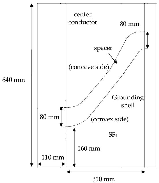
Figure 1.
The simulation geometry of the spacer.
- Ion current from the gas side and solid-side charge conduction
The calculation of the ion current in SF6 introduces the kinematic processes of radiative ionization, complexation, drift, and diffusion of charge carriers (Figure 2). In addition, only positive and negative ions are considered in the simulation to reduce computational complexity and improve model convergence performance []. The charge drift motion on the gas side is maintained by the electric field, while the diffusive motion is due to the local difference in charge carrier density. Therefore, the dynamic process of positive and negative charge carrier densities (n+ and n−) can be described by a set of drift-diffusion equations []:
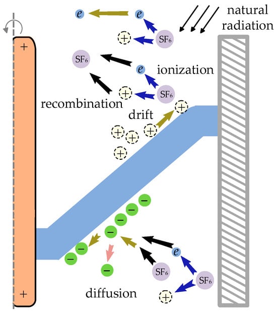
Figure 2.
The motion of ions on the gas side.
In Equation (1), t is the time. Sra represents the rate of positive and negative ions generated by ionization of SF6 molecules due to natural radiation; μ+ and μ− are the positive and negative ion mobility. D+ and D− represent the diffusion coefficients of positive and negative ions. The electric field strength E can be calculated based on the potential φ. The relationship between the potential and the space charge density ρ can be expressed by the Poisson equation as follows:
ε is the relative dielectric constant of the SF6, and e denotes the elementary charge.
The current density jg in SF6 is mainly determined by the conduction current density jcon_g under the combined influence of the ion drift motion caused by the applied electric field and the diffusion motion due to the difference in charge density. In addition, the displacement current density jdisp_g caused by the time-varying electric field in gas needs to be taken into account for the transient process. Thus, the ion current density jg in the gas phase can be expressed as follows:
D is the electric displacement vector.
The volume current density jb on the solid side of the spacer is likewise composed of a combination of conduction and displacement currents and can be described as follows []:
γv is the conductivity of the spacer bulk.
- Characterization of time-varying charges at the interface
The charge accumulation on the surface of the spacer is influenced by the current density on the spacer bulk side in the vertical direction (jbn), the vertical current density in the gas phase (jgn), and the leakage current on the spacer surface in the horizontal tangential direction (js), as shown in Figure 3. The surface leakage current and time-varying surface charge density ρs can be described as Equations (5) and (6) [] as follows:
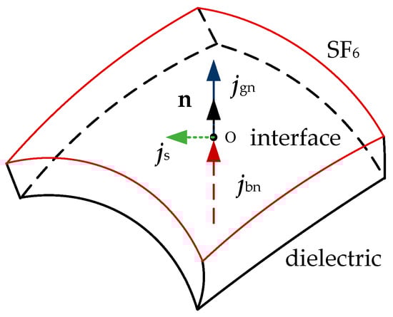
Figure 3.
The current densities on the gas–solid interface of the spacer.
The γS is surface conductivity, and Eτ is the tangential component of the electric field at the interface. n is the unit normal vector, and jbn and jgn are normal components of the current density on the spacer bulk side and gas side, respectively. In addition, the value of γS is considered as 10−19~10−20 [,], which is two orders of magnitude less than the conductivity of the spacer bulk. Thus, the leakage current density js in the tangential direction along the surface is usually negligible when the spacer surface is not specially modified to improve its surface conductivity []. Therefore, the tangential leakage current of the surface is not introduced in the model constructed in this paper [].
2.2. Boundary Conditions and Simulation Model Parameters
DC voltage VHV = 500 kV is applied to the center conductor, and VGND at the grounding shell is set to zero potential. The positive ion density at the junction of the SF6 with the center conductor is bound by the Dirichlet boundary condition, while the negative ion density at that side is bound by the Neumann boundary condition []. Similarly, the negative ion density at the intersection of the SF6 gas and the grounding shell is bound by the Dirichlet boundary condition, while the positive ions follow the Neumann boundary condition there []. The boundary conditions are set as in Table 1. The simulation model parameters are given as shown in Table 2.

Table 1.
Boundary condition.
Table 2.
Simulation model parameters.
3. Time-Varying Characteristics of Surface Charge
In this section, the current density, net current density flux, surface charge density, and surface electric field on the spacer during the transition of surface charge from an initial state to a steady state are investigated by simulation. The transfer mechanism between the accumulated charge and the current density on both sides is analyzed. In addition, the changes in the charge accumulation characteristics on the spacer surface are discussed by varying the conductivity of the dielectric and the gas-phase ion mobility, respectively.
3.1. Surface Charge Accumulation Characteristics
When the positive and negative ion mobility in SF6 and dielectric conductivity are set to the constants in Table 2, the time-varying normal current density, net current density flux, surface charge, and electric field on the concave and convex sides of the spacer are shown in Figure 4. Surface accumulation is a long-term process that needs to be considered on a large time scale, so 500 h, 1000 h, 2000 h, and 4000 h are taken as examples to discuss the charge distribution after different lengths of continuous operation.
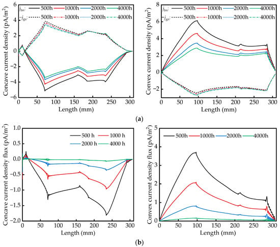
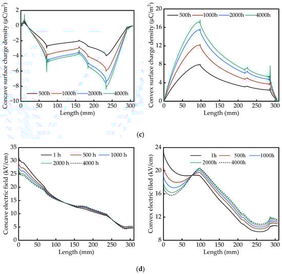
Figure 4.
Charge characteristic parameters of concave and convex surface of the spacer: (a) Current density; (b) Current density flux; (c) Surface charge; (d) Electric field. (The curves in the left column are the results of the concave side of the spacer, and the curves in the right column are the results of the convex side of the spacer).
As shown in Figure 4a, on both sides of the concave and convex surfaces of the spacer, the value of normal volume current density (jbn) on the spacer bulk side is larger in magnitude than the value of normal ion current density from the gas side (jgn). The normal current densities on both sides of the gas–solid interface are not continuous, leading to the presence of non-zero net current density fluxes (jbnjgn) (as shown in Figure 4b), which results in the phenomenon of charge accumulation on the demarcation surface. With the change of time, affected by the change of space electric field, the value of ion current density from gas-ion movement gradually increases, while the value of current density from dielectric gradually decreases, and the difference of current density on both sides of the interface diminishes, reaching the current densities on both sides of the gas–solid interface are matched until 4000 h. When the net current density flux tends to zero, the charge accumulated on the spacer also reaches a stable state, and its polarity is the same as the net current density flux in the previous transition process, as shown in Figure 4c. The convex surface of the spacer accumulates the positive polarity charges as the DC excitation is applied to the center conductor, while the concave surface deposits a positive polarity charge only in the small area immediately adjacent to the center conductor, and the rest of the area is covered by negative polarity charge.
On this basis, the inhomogeneous electric field formed by the special umbrella-skirt-like geometry of the spacer is further distorted under the influence of surface charge, as shown in Figure 4d. The electric field on the concave side appears to be “weakened on both ends and strengthened in the middle”, and the biggest reduction in the electric field appears in the region close to the center conductor, which is weakened by about 18.4% compared with the initial moment. The peak of the electric field enhancement occurs at the peak of negative charge convergence, with a maximum electric field increase of about 9.05%. In addition, the convex side of the spacer shows a peak of positive charge convergence at a horizontal distance of 100 mm from the center conductor due to the accumulation of single positive charges. The electric field strength in the region near the high-voltage side of the convex surface (up to 80 mm from the center conductor) is generally weakened, and the maximum electric field weakening can reach up to 26.3%. The increase in the electric field due to the deposition of space charge in the remaining convex regions is about 15%.
3.2. Effect of Dielectric Conductivity on Charge Accumulation
The spacer is often made of epoxy resin and alumina composite materials, and due to the differences in fabrication processes, material ratios, and component sizes, the conductivities of spacers commonly found in the existing studies have large differences [,,]. In this subsection, we model the charge accumulation on the surface of spacers with different conductivities and analyze the differences in the charge accumulation process of spacers under the two forms of gas current-dominated and solid-side charge transfer dominated.
According to Equation (5), it can be seen that in the process of surface charge accumulation, the charge transfer in dielectric and gas-phase charge deposition are in a mutual counteracting effect. Referring to the results of existing experimental studies [], five different levels of conductivity are discussed in correlated with the range of conductivity selected for spacers in existing studies [,,]: γv1 = 2 × 10⁻¹⁵ S/m, γv2 = 2 × 10⁻¹⁶ S/m, γv = 2 × 10⁻¹⁷ S/m, γv3 = 2 × 10⁻¹⁸ S/m, γv4 = 2 × 10⁻¹⁹ S/m, where γv is the conductivity of intermediate grade. When the charge movement at the gas–solid interface reaches a steady state, the surface charge on the surface of spacers with different conductivities is significantly different in polarity and amplitude, as shown in Figure 5a. Spacers with conductivity greater than γv have a little variation in the polarity and amplitude of the charges deposited on their surfaces. In contrast, the polarity of deposited charges on the surface of spacers with conductivity below γv is reversed, and the density of deposited charge increases substantially. This is due to the fact that when the spacer conductivity is greater than γv, the volume current density is still greater than the ion current density from the gas at this time, and the current density of both sides of the interface is similar to that in Figure 4. The polarity of the net current density flux does not change, so the polarity of the accumulated charge on the interface of solid and gas does not change, and it reaches a steady state with only a weak increase in charge density amplitude. In contrast, when the spacer conductivity is less than γv, the steady-state charge on the surface of the spacer not only changes polarity, but the density also increases substantially.
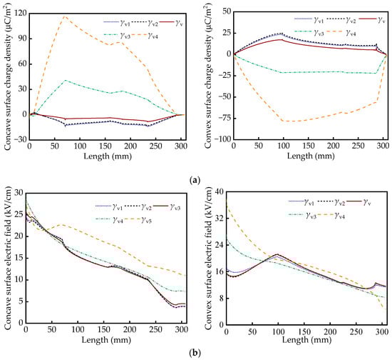
Figure 5.
Steady-state surface charge and electric field distributions on the surface of spacers under different conductivities: (a) Surface charge; (b) Electric field. (The curves in the left column are the results of the concave side of the spacer, and the curves in the right column are the results of the convex side of the spacer).
Since the volume current density jb in the bulk side is calculated from Ohm’s law (as Equation (4)), it is directly related to the spacer conductivity. The accumulated charge at the gas–solid interface is determined by both the gas side and the solid side. Therefore, when the conductivity of the dielectric increases, the volume current density directly increases, followed by the formation of a difference with the ion current density from the gas, which becomes the main source of the charge accumulated on the surface. The current density on the solid side is sensitive to changes in the weak electric field generated by charge deposition, and the volume current density decreases rapidly during space charge accumulation and matches the ion-current density on the gas side, allowing the charge on the interface of solid gas to reach a steady state more quickly.
Conversely, when the conductivity of the spacer decreases, the ion current density from the gas (jgn) is greater than the volume current density (jbn). And because the charge transferred from the gas to the interface has opposite polarity to the charge conducted from the spacer bulk, the net current density flux at the surface (jbn − jgn) is altered, reversing the polarity of the surface charge at the steady state. In addition, due to the number of carriers in the gas and the strong electric field environment, the current density on the SF6 gas side is difficult to decrease rapidly, and the volume current density in spacer bulk is difficult to increase rapidly due to the weak conductivity. As a result, it often takes longer to match the current density on both sides of the gas–solid interface at a low-conductivity spacer bulk, and the longer steady-state transition time in turn causes more charges to be deposited on the surface of the spacer. This result explains the differences in peak density as well as charge polarity between the surface charges obtained by Winter et al. [] based on lower spacer conductivity (10−19 magnitude) and those calculated by Du et al. [] and Luo et al. [] based on higher spacer conductivity (10−15 magnitude).
When the conductivity is large, solid-side charge conduction is the main source of surface charge, while when the conductivity is small, the surface charge relies mostly on charge deposition in the gas phase. Theoretically, there is a critical conductivity in which the effect of charge transfer in dielectrics counteracts that of gas-phase charge deposition under ideal conditions. Although the decrease in dielectric conductivity can increase the solid breakdown voltage, it also leads to the accumulation of more electric particles on the surface of the spacer, resulting in great distortion of the electric field, as shown in Figure 5b. Therefore, in order to make the surface charge density and surface electric field of the spacer relatively stable, the conductivity should be designed to stay as close as possible to the critical conductivity.
3.3. Effect of Ion Mobility in Gas-Phase on Charge Accumulation
In order to meet the insulation requirements under high voltage, GIS is usually filled with SF6. The mobility of positive and negative ions in SF6 is easily affected by pressure, temperature, and other conditions, which affect the charge accumulation process on the surface of the spacer. Especially when the temperature field is not uniformly distributed, ion mobility can be unevenly distributed with the temperature field. In this section, we first consider the impact of different constant values of ion mobility on charge accumulation under the ideal conditions of uniform temperature distribution and take the positive and negative ion mobility μ2+ = μ2− = 0.048 cm2/(V·s) set in Table 2 as the intermediate positive and negative ion mobility. According to the range of the positive and negative ion mobility under the influence of the pressure and the temperature [], the additional two different groups of the positive and negative ion mobility μ1+ = μ1− = 0.012 cm2/(V·s), μ3+ = μ3− = 0.084 cm2/(V·s) are added for simulation.
The surface charge distribution of the concave and convex surfaces of spacers under steady state is shown in Figure 6. With the increase in ion mobility, the charges deposited on the concave and convex surfaces of the spacer only increase slightly at the accumulation peak, and there is no reversal in charge polarity. This situation is mainly affected by two factors. One is the change in positive and negative ion mobility, which indirectly affects the ion flow in the gas phase by changing the rate of motion of ions in a strong electric field. Unlike changes in conductivity, changes in ion mobility cannot directly affect the normal current density on the gas side of the interface. Secondly, under a long simulation time span, the current density from the gas side is limited by the number of carriers in the gas-phase space, and changes in the charge migration rate still cannot lead to a rapid increase in the gas-phase current density. In addition, since the charge deposition on the surface of the spacer does not show significant change under steady state, the steady-state electric field along the spacer also does not change significantly for this variable.
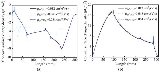
Figure 6.
Steady-state charge distributions on the surface of spacers under different ion mobilities: (a) Concave side; (b) Convex side.
4. Effect of Temperature Field on Charge Accumulation
Spacers typically operate in high-temperature environments. The heat generated by the direct current passed in the center conductor causes the temperature of the gas-solid system around the spacers to show a gradient distribution. On the one hand, the temperature gradient has an effect on the conductivity of the spacer bulk. On the other hand, the kinetic properties of charged particles in the SF6 also change with temperature. In this section, the surface charge accumulation characteristics of the spacer under the temperature field are explored, and the rules of surface charge accumulation under different temperature fields are analyzed.
4.1. Modeling of Temperature Field
The main modes of heat transfer around the spacer in DC-GIS are solid heat transfer and heat transfer fluid [,]. According to Fourier’s law, solid heat transfer is mainly through dielectric, and fluid heat transfer is mainly through SF6 gas convection. A partial differential equation containing a transient term, a heat convection term, a heat conduction term, and a heat source term is usually used to describe the heat transfer, as shown in Equation (7) as follows:
where ρ is the density of SF6 and the density of the spacer. Cp is the specific heat capacity of the object. T is the time-varying temperature. k is the thermal conductivity of the substance. u is the speed of movement of the fluid or the solid. t is the time. And q is the flux of heat transfer. The center conductor and the grounding shell of the DC-GIS are usually set up for the first type of boundary condition during rated operation [,], and typical boundary temperatures are usually set to Tc and Tw. In addition, the spacer is adjacent to SF6, so the boundary temperature and heat flux of the heat transfer model on the gas–solid demarcation plane are set as follows:
where Tup and Tdown are the boundary temperatures above and below the spacer interface. qup and qdown are fluxes of heat transfer on both sides of the spacer interface. The key thermal field simulation parameters are shown in Table 3.
Table 3.
Thermal field simulation model parameters.
In addition, the correspondence between the bulk conductivity, the ion mobility of SF6, and the temperature can be fitted as Equation (9):
4.2. Surface Charge under Temperature Gradient Distribution
The two-dimensional temperature distribution around the spacer under DC excitation is shown in Figure 7a. In the initial stage of heat transfer, the heat field distribution shows an extremely inhomogeneous state, and the heat transfer process along the basin is slower than the gas heat transfer. This is due to the fact that the epoxy resin-based composite material has a higher density as well as a larger specific heat capacity compared to the SF6 gas, and thus the basin temperature change rate is slower with the same thermal field boundary conditions and heat source. Finally, at about 17 h, the thermal field around the spacer basically reaches a stable and uniform state.
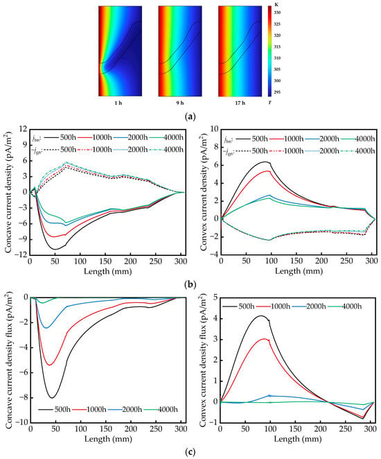
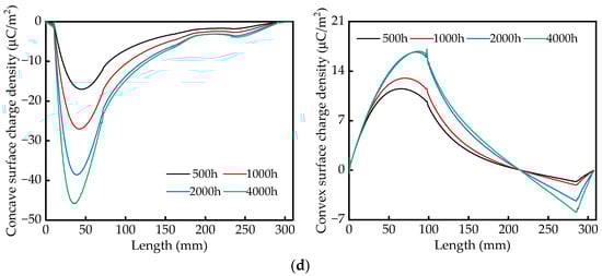
Figure 7.
Time-varying thermal field distributions and charge characteristic parameters under temperature field: (a) Time-varying thermal field; (b) Current density; (c) Current density flux; (d) Surface charge. ((b–d): The curves in the left column are the results of the concave side of the spacer, and the curves in the right column are the results of the convex side of the spacer).
Compared with the results without considering the temperature field, there is a significant increase in the value of the volume current density jbn in the region center conductor nearby under the temperature gradient distribution, while the value of the normal ion current density in gas-phase jgn is not significantly changed (as shown in Figure 7b). Therefore, the net current density flux values (jbn − jgn) on concave and convex surfaces surge in the near-center conductor region of the spacer (as shown in Figure 7c). The polarity of the charge attached to the spacer surface is still determined by the net current density flux, as shown in Figure 7d. The concave surface deposits predominantly space charges with negative polarity. On the convex surface, only a small number of negative particles are attached to the region adjacent to the grounding shell, and the rest of the area is covered with positive charges. Compared with the surface charge distribution in Section 2.1, the peak of surface charge accumulation under the temperature gradient field increases and is mainly concentrated in the high-temperature region. The polarity of the charge on the convex side of the spacer near the grounded shell is reversed.
Influenced by the temperature field, the conductivity of the spacer and the temperature increase from the grounding shell side to the center conductor side. As the conductivity of the spacer surges rapidly as an exponential variation with temperature [,], this current density in the spacer bulk side (jbn) adjacent to the center conductor grows significantly as well. Additionally, the normal current density on the gas side (jgn) is relatively less affected by the rising ion mobility. Thus, the net flux value of the current density on the interface, jbn − jgn, is mainly concentrated on the region near the center conductor, which increases the steady-state spacer surface charge density. The simulation results are consistent with the conclusion found experimentally by Li et al. [] that more volume charges from the solid side accumulate on the surface of the dielectric in the high-temperature region. On the region adjacent to the grounding shell, the low-temperature variation makes the change in the conductivity of the spacer not obvious, and the current density in the gas phase is slightly larger than the value of the current density in the spacer side, which leads to the reversal of the polarity of the charge accumulated on the convex surface close to the grounding shell.
4.3. Characterization of Surface Charge Distribution under Different Temperature Environments
The internal temperature of DC-GIS mainly depends on the current value in the conductor, and different current values correspond to different temperature distributions in the gas–solid phase system. This section mainly introduces three reasonable steady-state central conductor temperatures, which are 295 K, 333 K, and 363 K, respectively. The grounding shell temperature is still 293 K. Therefore, the temperature difference between the central conductor and the grounding shell is ΔT1 =2 K, ΔT2 = 40 K, and ΔT3 = 70 K, respectively [,]. The steady-state temperature distribution on the interface between SF6 gas and the spacer bulk is shown in Figure 8. The closer to the center conductor on the insulating medium, the higher the temperature field on its surface. The temperature gradient between the central conductor and the grounding shell increases as the temperature difference between the conductor and the grounded shell increases. Under different temperature differences, there are obvious differences between the charge distributions on the concave and convex surfaces of spacers at steady state, as shown in Figure 9. The peak value of charge accumulation on the concave side increases continuously with the increase in temperature difference, and the high-density charge accumulation area also gradually moves to the high-temperature area. For the convex side, although the increase in temperature difference slightly increases the peak value of steady-state charge accumulation, the change in magnitude is not significant.
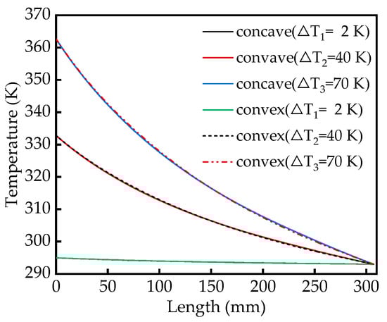
Figure 8.
Steady-state temperature along the surface of the spacer under different temperature fields.
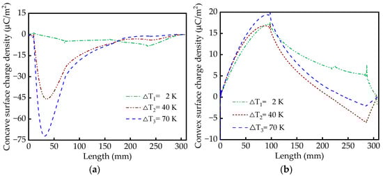
Figure 9.
The steady-state surface charge distributions: (a) Surface charge density on the concave side; (b) Surface charge density on the convex side.
In addition, the increase in temperature difference greatly increases the conductivity of the spacer, creating a highly conductive region similar to the “insulation failure zone” []. Therefore, the steady-state charge density near the center conductor increases. However, due to the large amounts of negative charges accumulated around the center conductor of the convex surface under the effect of the electric field, the net current density flux on the interface does not change significantly when the volume current density of the convex side increases.
5. Conclusions
This paper builds a surface charge accumulation model of a spacer, studies the relationship between the surface charge and charge transfer in the gas/solid phase, and analyzes the influences of dielectric conductivity, gas ion mobility, and temperature field on the surface charges. The following conclusions are reached:
The reason for the surface charge accumulation on the spacer is that the volume current density on the solid side and the ion current density from SF6 are discontinuous. There is a net flux of current density on the surface of the spacer, resulting in the accumulation of surface charges. Space charges that accumulate on the interface affect the surrounding electric field, so that the current density difference between the two sides of the interface continuously decreases, and eventually reaches a steady state.
Changes in conductivity affect the volume current density and the current density flux at the interface, leading to variations in the polarity and density of surface charge. When the conductivity is large, charge transfer in the dielectric is the main source of surface charge, and the volume current density is sensitive to changes in the electric field. The electric field generated by surface charge can quickly reduce the volume current density so that the surface charge rapidly processes to a stable state. When the conductivity is small, the bulk current density decreases, the surface charge mostly relies on gas phase charge deposition, and the net flux polarity of the interface current density changes. More interface charges need to be deposited on the interface to reduce the ion current density from the SF6, resulting in a dramatic increase in the amplitude of the charge density as well. Theoretically, there is a critical conductivity in which the effect of charge transfer in dielectrics counteracts that of gas-phase charge deposition to avoid the occurrence of surface charge.
The effect of ion mobility is related to the temperature field. When the temperature is uniformly distributed, the ion mobility has little impact on the polarity and peak value of the accumulated charge, which is limited by the number of ions and is unable to directly affect the current density of the gas. Under the temperature gradient distribution, due to the influence of ion mobility and temperature rise on the near-grounding shell, the ion current density from the gas side increases, even greater than the volume current density, causing the polarity of the accumulated charge in this area to reverse.
The effect of the temperature on the charge accumulation is mainly realized by affecting the dielectric conductivity and ion mobility. Under the temperature gradient distribution, the dielectric conductivity on the near-center conductor side increases sharply, resulting in a surge in the volume current density, while the gas-phase ionic current is not significantly changed as the temperature rises. Thus, the current density difference on the interface becomes larger, and the surface charge accumulated in this high-temperature region reaches a higher amplitude.
For the aspect of design, in order to make the current density on both sides of the interface as balanced as possible, the conductivity of spacer bulk near the center conductor can be designed to be smaller, while the value of conductivity near the side of the grounding shell can be larger so that the distribution of the current density fluxes on the surface of the spacer is more uniform under the influence of the temperature field. Moreover, the accumulated charge density is higher on the side near the center conductor, and components such as extra shielding rings may need to be added to suppress electric field distortions in that area.
Author Contributions
Conceptualization, Y.L. and H.J.; methodology, Y.L. and H.J.; validation, Y.L. and H.J.; formal analysis, Y.L. and H.J.; investigation, Y.L. and H.J.; resources, H.J.; writing—original draft preparation, Y.L.; writing—review and editing, Y.L. and H.J.; visualization, Y.L. and H.J.; supervision, Y.H. and J.T. All authors have read and agreed to the published version of the manuscript.
Funding
This research was funded by the National Key Research and Development Program of China (Grant number: 2021YFB2401700) and National Natural Science Foundation of China (Grant No. 52377135).
Data Availability Statement
All the data supporting the reported results have been included in this paper.
Conflicts of Interest
The authors declare no conflicts of interest.
References
- Straumann, U.; Schuller, M.; Franck, C. Theoretical investigation of HVDC disc spacer charging in SF6 gas insulated systems. IEEE Trans. Dielectr. Electr. Insul. 2013, 19, 2196–2205. [Google Scholar] [CrossRef]
- Li, C.; Lin, C.; Cheng, G.; Zhang, Z.; Zhang, L.; He, J. Review of gas-solid interface charging phenomena of HVDC spacers. Proc. CSEE 2020, 40, 2016–2026. [Google Scholar]
- IEEE Substations Committee Working Group K4. Partial discharge testing of gas insulated substations. IEEE Trans. Power Deliv. 1992, 7, 499–506. [Google Scholar] [CrossRef]
- Cao, Y.; Liu, X.; Liu, D.; Wang, E. Investigation of a dynamic neural network approach and its application of multivariable optimization to electrical apparatus. Proc. CSEE 2006, 26, 112–116. [Google Scholar]
- Ma, A.; Yang, X.; Lu, X.; Jiang, X. 3D electric field calculation and its inverse problem analysis of disk-type insulator in GIS. High Volt. Eng. 2010, 36, 1217–1221. [Google Scholar]
- Du, J.; Zhang, S.; Li, N.; Peng, Z. Electric field distribution calculation and shielding electrode structure optimization of UHVAC basin-type insulator. High Volt. Eng. 2013, 39, 3037–3043. [Google Scholar]
- Jia, Y.; Gao, L.; Ji, S.; Cheng, Y.; Liu, W. Comprehensive optimization of electrical and mechanical performance of 1100 kV basin-type insulator based on genetic algorithm and finite element simulation. High Volt. Eng. 2019, 45, 3844–3853. [Google Scholar]
- Xu, H.; Sima, W.; Sun, P.; Shao, Q.; Xu, J.; Li, C. Effect of surface charge on electron multiplication process of ER/SF6 interface. High Volt. Eng. 2022, 48, 1716–1725. [Google Scholar]
- Li, S.; Yin, G.; Bai, S.; Li, J. A new potential barrier model in epoxy resin nanodielectrics. IEEE Trans. Dielectr. Electr. Insul. 2011, 18, 1535–1543. [Google Scholar] [CrossRef]
- Wang, W.; Min, D.; Li, S. Understanding the conduction and breakdown properties of polyethylene nanodielectrics: Effect of deep traps. IEEE Trans. Dielectr. Electr. Insul. 2016, 23, 564–572. [Google Scholar] [CrossRef]
- Li, J.; Liang, H.; Du, B.; Wang, Z. Surface functional graded spacer for compact HVDC gaseous insulated system. IEEE Trans. Dielectr. Electr. Insul. 2019, 26, 664–667. [Google Scholar] [CrossRef]
- Shao, T.; Liu, F.; Hai, B.; Ma, Y.; Wang, R.; Ren, C. Surface modification of epoxy using an atmospheric pressure dielectric barrier discharge to accelerate surface charge dissipation. IEEE Trans. Dielectr. Electr. Insul. 2017, 24, 1557–1565. [Google Scholar] [CrossRef]
- Yan, W.; Li, C.; Lei, Z.; Han, T.; Zhang, Z.; Fabiani, D. Surface charging on HVDC spacers considering time-varying effect of temperature and electric fields. IEEE Trans. Dielectr. Electr. Insul. 2019, 26, 1316–1324. [Google Scholar] [CrossRef]
- Du, B.; Dong, J.; Liang, H. Electric field control by permittivity functionally graded and superficially non-linear conductivity materials for DC-GIS spacer. High Volt. 2022, 7, 992–1000. [Google Scholar] [CrossRef]
- Zhou, H.; Ma, G.; Li, C.; Shi, C.; Qin, S. Impact of temperature on surface charges accumulation on insulators in SF6-filled DC-GIL. IEEE Trans. Dielectr. Electr. Insul. 2017, 24, 601–610. [Google Scholar] [CrossRef]
- Li, C.; Deng, B.; Zhang, Z.; Yan, W.; Li, Q.; Zhang, Z.; Lin, C.; Zhou, Y.; Han, T.; Lei, Z.; et al. Full life property of surface charge accumulation on HVDC spacers considering transient and steady states. IEEE Trans. Dielectr. Electr. Insul. 2019, 26, 1686–1692. [Google Scholar] [CrossRef]
- Shimakawa, H.; Kumada, A.; Hidaka, K.; Sato, M.; Yasuoka, T.; Hoshina, Y.; Shiiki, M. One-dimensional modeling of charge transport in epoxy for DC-GIS insulating spacer. IEEE Trans. Dielectr. Electr. Insul. 2021, 28, 1457–1464. [Google Scholar] [CrossRef]
- Zhang, B.; Qi, Z.; Zhang, G. Charge accumulation patterns on spacer surface in HVDC gas-insulated system: Dominant uniform charging and random charge speckles. IEEE Trans. Dielectr. Electr. Insul. 2017, 24, 1229–1238. [Google Scholar] [CrossRef]
- Volpov, E. Electric field modeling and field formation mechanism in HVDC SF6 gas insulated systems. IEEE Trans. Dielectr. Electr. Insul. 2003, 10, 204–215. [Google Scholar] [CrossRef]
- Lutz, B.; Kindersberger, J. Surface charge accumulation on cylindrical polymeric model insulators in air: Simulation and measurement. IEEE Trans. Dielectr. Electr. Insul. 2011, 18, 2040–2048. [Google Scholar] [CrossRef]
- Winter, A.; Kindersberger, J. Stationary resistive field distribution along epoxy resin insulators in air under DC voltage. IEEE Trans. Dielectr. Electr. Insul. 2012, 19, 1732–1739. [Google Scholar] [CrossRef]
- Yang, W.; Zhu, T.; Tian, Y.; Yang, X.; Zhu, S.; Ye, J. Charge accumulation and electric field transition characteristics of basin insulator under DC voltage. High Volt. Eng. 2020, 46, 1978–1985. [Google Scholar]
- Jiang, H.; Li, W.; Xu, Y.; Liu, H.; Tan, J.; Shao, T. Influence of segmented grounding electrodes on electrical characteristics in annular surface dielectric barrier discharge. J. Phys. D Appl. Phys. 2021, 54, 265203. [Google Scholar] [CrossRef]
- Wiegart, N.; Niemeyer, L.; Pinnekamp, F.; Kindersberger, J.; Morrow, R.; Zaengl, W.; Zwicky, M.; Gallimberti, I.; Boggs, S. Inhomogeneous field breakdown in GIS-the prediction of breakdown probabilities and voltages. Part I. IEEE Trans. Power Deliv. 1988, 3, 939–946. [Google Scholar] [CrossRef]
- Luo, Y.; Tang, J.; Pan, C.; Pan, Z.; Li, Y.; Cui, Z. Dynamics of surface charge and electric field distributions on basin-type insulator in GIS/GIL due to voltage polarity reversal. High Volt. 2020, 5, 151–159. [Google Scholar] [CrossRef]
- Schueller, M.; Straumann, U.; Franckc, C. Role of ion sources for spacer charging in SF6 gas insulated HVDC systems. IEEE Trans. Dielectr. Electr. Insul. 2014, 21, 352–359. [Google Scholar] [CrossRef]
- Morrow, R. A survey of the electron and ion transport properties of SF6. IEEE Trans. Plasma Sci. 1986, 14, 234–239. [Google Scholar] [CrossRef]
- Li, C.; Hu, J.; Lin, C.; He, J. The potentially neglected culprit of DC surface flashover: Electron migration under temperature gradients. Sci. Rep. 2017, 7, 3271. [Google Scholar] [CrossRef]
Disclaimer/Publisher’s Note: The statements, opinions and data contained in all publications are solely those of the individual author(s) and contributor(s) and not of MDPI and/or the editor(s). MDPI and/or the editor(s) disclaim responsibility for any injury to people or property resulting from any ideas, methods, instructions or products referred to in the content. |
© 2024 by the authors. Licensee MDPI, Basel, Switzerland. This article is an open access article distributed under the terms and conditions of the Creative Commons Attribution (CC BY) license (https://creativecommons.org/licenses/by/4.0/).