1. Introduction
Deep learning technology has achieved groundbreaking advancements in several artificial intelligence subfields, including natural language understanding, computer vision, and reinforcement learning. Convolutional neural networks (CNNs) have emerged as pivotal tools for managing a wide range of complex tasks within these areas. They are instrumental in applications such as image recognition, natural language processing, vision systems in autonomous vehicles, and the analysis of medical imagery. CNNs excel at processing massive quantities of high-dimensional data with remarkable precision and efficiency. However, these sophisticated models often require significant computational storage and energy; this is manageable in data centers or on high-performance computing platforms, but it becomes a substantial hurdle for resource-limited edge devices like smartphones, embedded systems, and wearable technology. This challenge has spurred increased interest in the development of neural network hardware accelerators, particularly those that utilize bit-serial computation techniques. These accelerators are designed to optimize performance and efficiency, making advanced neural network applications more accessible on a wider range of devices.
Bit-serial computation is a distinctive arithmetic approach that processes each bit of a number sequentially, one at a time. This method starkly contrasts with the traditional bit-parallel technique in which multiple bits are processed together within the same clock cycle. In bit-serial computation, numbers are broken down into individual bits, each handled over multiple clock cycles. This approach is a strategic balance between time and space considerations. The primary advantage of bit-serial computation lies in its significant reduction of hardware resource requirements. By processing a single bit at a time, it reduces the size of the necessary storage and arithmetic logic units, making it ideal for scenarios with limited hardware resources or in which cost efficiency is crucial. Moreover, the reduced complexity of computational circuitry inherent in processing one bit at a time leads to lower power consumption. This is particularly advantageous for battery-powered mobile and embedded devices, where power efficiency is a key concern. Despite these benefits, bit-serial computation faces certain limitations and challenges. One of the main issues is the potential increase in computational delays due to the bit-by-bit processing method. Additionally, while the bit-serial method can decrease the width of data, it may impact the precision of computations. Therefore, finding a suitable quantization strategy is essential to ensure that any reduction in computational accuracy remains within acceptable boundaries while simultaneously minimizing data width.
Bit-serial CNN hardware accelerators consist of a processing element array (PEA), memory, and control units. In this setup, each bit-serial processing element (PE) within the array is tasked with computing a convolution kernel. These PEs are equipped with several multiply–accumulate units (MACs) which are interconnected in a specific form. The system processes input feature maps (IFMs) and weights in a bit-serial manner, channeling them through the MACs and PEs. By adopting the bit-serial method, data width is minimized, facilitating the use of fixed-point rather than floating-point arithmetic, which in turn simplifies the hardware complexity.
Bit-serial neural network accelerators provide an effective solution for applications in deep learning that demand a compact size and low power consumption. The key contributions of this paper include the following:
A streamlined quantization formula and the introduction of a preprocessing method for quantization which allows for the removal of bias data;
The development of a column-buffering (CB) dataflow designed to reduce the need to access and move the IFM;
The design of a convolutional layer processing element array (CL PEA) unit architecture. This architecture leverages an enhanced bit-serial MAC and is based on the proposed CB dataflow, culminating in the construction of a whole neural network accelerator.
The structure of the remaining sections of the paper is as follows:
Section 2 introduces related works.
Section 3 provides essential background knowledge, including an overview of CNN structures, the timing of bit-serial computation, and simplified quantization methods.
Section 4 details the operational process of the proposed CB dataflow.
Section 5, adopting a top-down approach, discusses the overall architecture of the neural network accelerator, encompassing the structure and function of the PEA, PE, and MAC components.
Section 6 focuses on the implementation, assessment, and prototype validation of the accelerator. Finally,
Section 7 concludes the entire paper.
2. Related Works
To address the challenges of high computational complexity and substantial area and power consumption, ESSA [
1] has implemented a suite of innovative strategies. These include a ring streaming dataflow which optimizes data movement; a data reuse strategy to minimize the need for new data inputs; bit reduction to decrease computational load by reducing data precision; loop tiling, a programming technique for boosting computational efficiency; and converting non-unit stride to unit stride to streamline the data processing workflow. Together, these optimizations significantly enhance computational performance and energy efficiency. The UNPU [
2] stands out as the first application-specific integrated circuit (ASIC) DNN accelerator capable of supporting fully variable weight precision ranging from 1 to 16 bits. This versatility allows the UNPU to fine-tune energy consumption while maintaining accuracy, striking an ideal balance between the two. Stripes [
3], on the other hand, tailors computation time to the precision level of the bit-serial computing unit. It capitalizes on the unique properties of bit-serial computing units and the natural parallelism in DNNs to improve performance and energy efficiency, all while preserving accuracy. This is achieved by dynamically adjusting the computation time in response to the required precision level. Previously, weight pixels were serially input into gate circuits, and IFM pixels were fed in parallel. Although effective, there was still potential for improvement. Our approach differs by serially feeding both IFM pixels and weight pixels into the gate circuits. This method further reduces the hardware footprint and energy consumption without compromising accuracy and maintains a high operational frequency.
Neural network accelerators typically adopt one of two architectures for their convolution arrays: temporal [
4] or spatial [
5,
6]. These are represented by a tree structure and a PEA, respectively [
7]. In bit-serial computing, effectively reusing data can considerably decrease the number of memory accesses, thereby reducing power consumption. For instance, in a PEA architecture, each computational unit is operation is controlled by the dataflow. Identifying an efficient dataflow is crucial for defining the spatial structure of the PEs and the overall PEA. There are four common dataflows [
8]: no local reuse (NLR) [
4,
9], input stationary (IS) [
10], output stationary (OS) [
11,
12], and weight stationary (WS) [
6,
13]. The NLR dataflow, typically implemented in a tree structure, does not reuse data, leading to higher hardware costs. In contrast, the other three dataflows are mainly used in PEAs. The IS dataflow reuses the same activations multiple times but overlooks significant output parallelism, resulting in increased total data access. The OS dataflow aims to minimize the energy used in reading and writing partial sums, yet it involves a substantial amount of external data access [
14]. The WS dataflow, on the other hand, minimizes the energy cost of reading weights due to its low data access and delivers average computational performance. The WS dataflow benefits from a multilevel memory hierarchy that enhances energy efficiency by reducing data access. To address the challenge of maximizing data reuse, we propose a CB dataflow inspired by the WS dataflow alongside an optimized PE structure.
To achieve performance gains and support a broad spectrum of applications, neural network accelerator systems often employ a hybrid approach, combining general-purpose processors with specialized accelerator logic. The general-purpose processor is tasked with executing operations that are inefficient for reconfigurable logic, such as handling data-dependent controls and memory access tasks. Traditional neural network accelerator systems can be broadly segmented into five types of coupling relationships with the general-purpose processor, as illustrated in
Figure 1.
The first type of coupling [
15] integrates the accelerator as a functional unit within the main processor, establishing a close integration. In this setup, the main processor regards the hardware accelerator as an internal module, delegating specific instructions to the accelerator for execution. The second coupling style [
16,
17], in which the hardware accelerator serves as an extension to the main processor, features an independent coprocessor dedicated to particular computational tasks. This arrangement helps offload tasks from the main processor. In the third coupling variant [
18,
19,
20,
21,
22,
23], the system incorporates an auxiliary processing unit which is essentially a dedicated processor with its own instruction set. This additional unit, which is directly linked to the main processor’s cache, enables swifter data access. The accelerator’s independent instruction set and programming space allow it to specialize in certain tasks, consequently freeing up resources in the main processor. The fourth coupling approach [
24] positions the accelerator within the input/output (I/O) channel, integrating it into the I/O system. This configuration allows the accelerator to manage I/O-related tasks, while the main processor treats it as a part of the storage access system. Being embedded in the I/O system, the accelerator can quickly respond to external signals and data, enhancing the efficiency and speed of data processing.
The fifth and final coupling relationship [
25,
26,
27,
28,
29,
30] is characterized by a separate, independent hardware architecture external to the I/O system. This distinct hardware setup provides increased modularity and flexibility. With data circulating through dedicated hardware, processing tasks can proceed autonomously without needing intervention from the main processor, thus boosting the overall system efficiency. Additionally, this configuration alleviates the burden on the main processor, allowing it to concentrate on other computational tasks. Owing to its flexibility, our neural network accelerator architecture adopts this fifth coupling model.
3. Preliminaries
3.1. CNN Basics
CNNs are a specialized type of deep learning algorithm predominantly utilized for processing grid-structured data, like images. CNNs adeptly and efficiently extract high-level features from raw data by employing a blend of convolutional layers (CLs), pooling layers, and fully connected layers (FCLs). This unique structure makes CNNs highly effective in a range of visual tasks, including image classification, object detection, and image generation. A significant advantage of CNNs over traditional fully connected networks is their ability to drastically reduce the number of parameters in the model. This reduction is achieved through local connections and weight sharing, substantially lowering the likelihood of overfitting. A notable example of an early CNN is LeNet-5, developed by Yann LeCun in 1998 [
31]. This pioneering model demonstrated remarkable success in recognizing handwritten digits and played a pivotal role in shaping the design of subsequent CNNs. As illustrated in
Figure 2a, the architecture of LeNet-5 mainly comprises two CLs, two pooling layers, and three FCLs.
Figure 2b shows a detailed view of a CL, and
Figure 2c provides a schematic representation of an FCL.
The CL is a fundamental component of CNNs. Its key role is to extract features that are locally relevant from input data. Unlike FCLs, convolutional operations are characterized by parameter sharing and local connections. This design enables the network to learn the local structures of high-dimensional data, such as images, more efficiently. Within a CL, the input matrix or tensor
I interacts with the convolutional kernel or filter
K through convolution operations to generate an output matrix or tensor
O. In a 2-D context, this convolutional operation is defined as in (1).
where
i and
j represent the indices of elements in the output feature map (OFM) matrix
O, while
m and
n denote the indices of elements in the convolution kernel
K. The dimensions of the convolution kernel are represented by
a and
b. The term
I refers to the IFM matrix. The stride, denoted as
s, dictates the movement interval of the convolution kernel over the input matrix, with larger strides leading to smaller output dimensions. The bias term
b is added to the convolutional output. After the addition of bias, models typically proceed to further processing with a nonlinear activation function like the Rectified Linear Unit (ReLU) function.
Pooling layers are integral parts of CNNs, primarily serving to reduce the size of feature maps and to cut down on the model’s computational demands. In these layers, a defined window size traverses the IFM or matrix
I, generating a single output value for each window which collectively form the OFM
O. The most prevalent types of pooling operations are max pooling and average pooling. Specifically, LeNet-5 employs max pooling. In max pooling, the output for each window is the maximum value found within it, as in (2).
where
i and
j denote the indices of elements in the OFM
O, while
k represents the size of the pooling window.
I refers to the IFM. Typically devoid of learnable parameters unless a learnable pooling method is used, pooling layers contribute to a reduction in the total parameter count of the network. This reduction is crucial for mitigating the risk of overfitting in the model.
The FCL, also known as a dense layer, is a staple in various types of neural networks, including traditional artificial neural networks, CNNs, and other deep learning architectures. Its main role is to execute nonlinear transformations and decision-making tasks. In an FCL, every output neuron is interconnected with all neurons in the input layer. From a mathematical standpoint, the operations of an FCL are represented by matrix multiplication followed by the addition of a bias term, as in (3).
where
I denotes the input vector or matrix,
W is the weight matrix,
b represents the bias vector, and
O is the output vector or matrix. The weight matrix
W and the bias vector
b are the learnable parameters of the layer. If the input layer consists of n neurons and the output layer comprises m neurons, the weight matrix
W of the FCL will contain
n ×
m parameters, while the bias vector
b will have
m parameters. Typically, the output from a fully connected layer undergoes a nonlinear transformation through an activation function like the ReLU function.
3.2. Bit-Serial Computing Basics
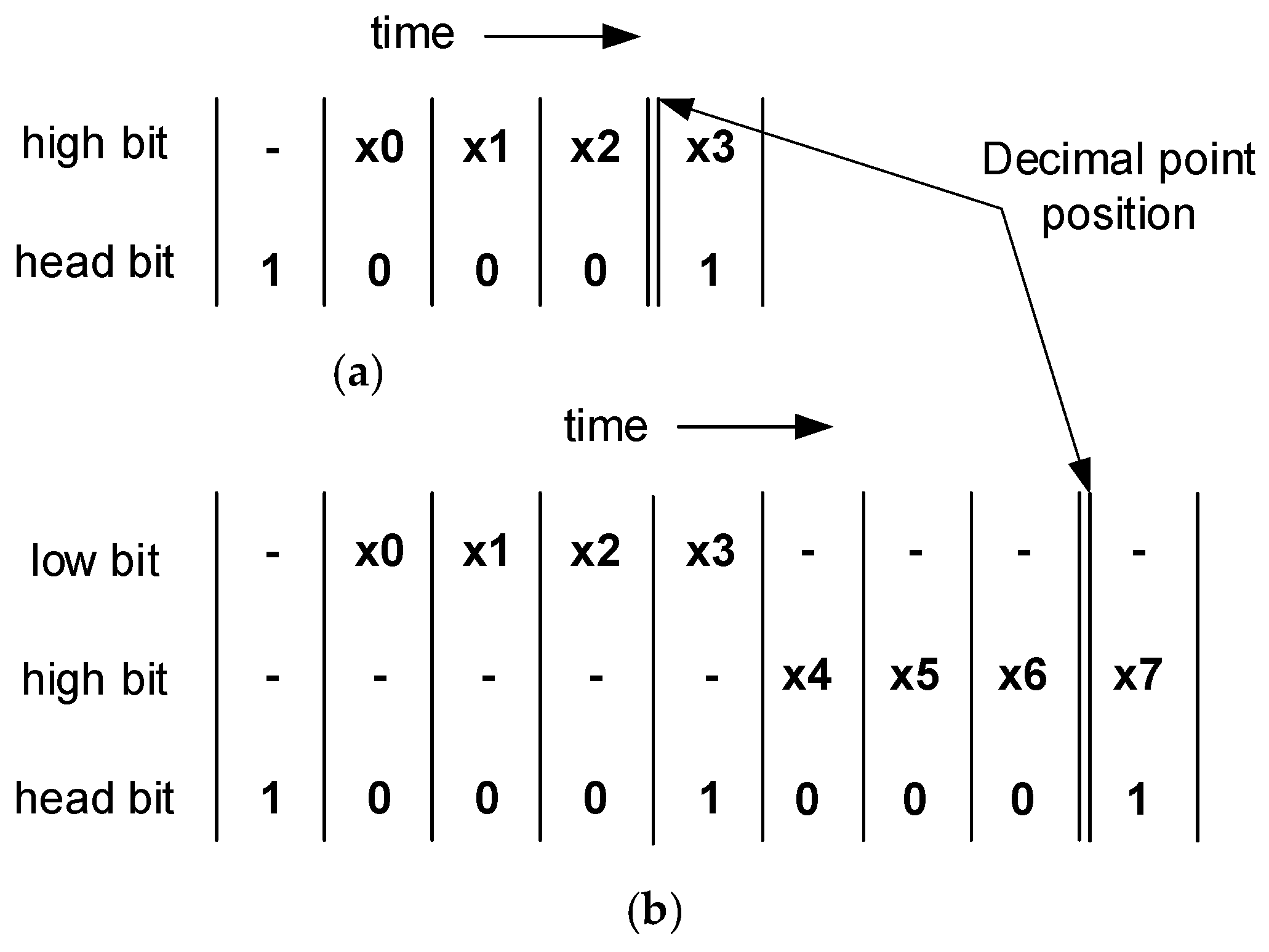
In representing fixed-point binary signed data, two’s complement is used to define two distinct data types: single precision and double precision [
32]. To represent binary numbers with varying dynamic ranges and levels of precision, different quantities of data lines are employed. With a data bit count
P of 4, the specific structures and timing for these two data types are illustrated in
Figure 3. The decimal point is positioned between the most significant bit (MSB) and the second-most-significant bit, with the least significant bit (LSB) being transmitted initially. Single-precision data are composed of a sign bit and
P − 1 fractional bits, while double-precision data include a sign bit and 2
P − 1 fractional bits. The role of bit-serial operators extends beyond calculating output bits; they are also tasked with generating control bits for output data. These control signals, associated with each data bit, are termed head bits.
The bit-serial multiplier processes one bit from one of the operands in each cycle, keeping the other operand fixed, and generates a partial product for that specific bit. This procedure is carried out for each bit in the operand, leading to the final product being the sum of all these partial products. Similarly, the bit-serial adder operates on a bit-by-bit basis. The MAC operation incorporates both multiplication and accumulation. A bit-serial MAC would integrate the functions of a bit-serial multiplier and a bit-serial adder. During each cycle, the multiplier creates a partial product, which is then passed to the accumulator to update the overall sum. This cycle repeats for each bit in the operands. Considering the significant decreases in area and power, we refer to Isshiki’s work on bit-serial multipliers and adders [
32].
3.3. Quantization
After successfully training the LeNet-5 model, we acquired the trained model parameters, namely weights and biases, and noted a training accuracy of 99.45%. Subsequently, we fed the test dataset into this trained model, following the Test1 step shown in
Figure 4a, which yielded an inference accuracy of 98.95%. Test1 employed the PyTorch framework to carry out forward inference using FP32 parameters—weights (W) and biases (B)—that were trained in the Training stage. The next phase involved the quantization of the trained model. Quantization is the process of performing computations and storing tensors at a lower bit width than floating-point precision. It entails operating on tensors at a lower precision rather than full precision. This approach enables more compact model representation and the utilization of high-performance vectorized operations across numerous hardware platforms.
For LeNet-5’s model quantization, we employed PyTorch’s quantization interface [
33]. PyTorch’s support for signed 8-bit integer (INT8) quantization, in contrast to standard 32-bit floating-point (FP32) models, allows for reductions in model size and memory bandwidth requirements by a factor of four. Hardware support for INT8 computations typically offers a speed advantage two to four times greater than FP32 computations. PyTorch provides several methods for quantizing deep learning models. Generally, models are trained in FP32 and then converted to INT8. PyTorch supports three main quantization modes: Dynamic Quantization, Post-Training Static Quantization (PTSQ), and Quantization-Aware Training. Given that our strategy involved statically quantizing both the activations and weights of the trained LeNet-5 model without the need to simulate quantization during training and using training data to concurrently learn quantization parameters, we opted for PTSQ as our quantization strategy. This strategy primarily utilizes symmetric quantization techniques.
Quantization results in converting each convolutional and fully connected layer into INT8 format for IFMs, OFMs, and weights while leaving biases unquantized. These parameters are then utilized as inputs for inference in the quantized model, as depicted in the Test2 step in
Figure 4a. Test2 conducts forward inference by batch-inputting IFMs and manually executing a sequence of operations—convolution, activation, pooling, or fully connected operations—layer by layer. This process uses data from INT8 parameters that have been quantized in the PyTorch Quantization stage: IFMs (A), weights (W), and biases (B). To maintain inference accuracy following the INT8 convolution, biases are retained in an FP32 format and are combined with the inner feature maps. This combination produces an FP32 OFM which is subsequently transformed back into an INT8 OFM through symmetric quantization marked as subscript q. Recognizing the challenges of implementing the Test2 step with hardware, the formula for symmetric quantization has been streamlined as in (4).
Upon examining the exported biases, as depicted in
Figure 4b, it becomes apparent that all the biases round to zero, suggesting the redundancy of the bias term. As a result, in the Test3 step, it is sufficient to convolve or multiply the INT8 IFM and weights and then directly convert the result into an INT8 OFM via symmetric quantization. This OFM can then serve as the input for subsequent convolutional or fully connected layers, facilitating continuous inference. The distinction between Test3 and Test2 lies in the omission of the bias term, enhancing the process’s simplicity and efficiency.
Overall, Test1 exhibits relatively lower complexity by leveraging the well-established PyTorch framework for its computations. This stage, while it utilizes FP32 parameters, provides higher accuracy but may fall short of the efficiency in computation and storage offered by INT8 parameters. In contrast, Test2 involves a higher degree of complexity due to the necessity of manually managing each layer, such as convolution and fully connected processes. Employing INT8 parameters, Test2 achieves greater efficiency in both computation and storage, albeit at the potential cost of reduced accuracy. In terms of complexity, Test3 is similar to Test2, yet the removal of bias terms lightens the computational burden.
The process of this simplification is outlined in
Figure 4c. Using LeNet-5, AlexNet, and VGG-16 as case studies,
Table 1 presents the accuracies achieved during various stages of training, testing, and quantization. After training on the MNIST dataset, all three CNN models reached notable levels of training and inference accuracy. Notably, the inference accuracies between Test2 and Test3 were almost indistinguishable, attesting to the efficacy of our streamlined quantization approach. Based on these findings, we will develop accelerators utilizing 8-bit bit-serial MACs for the applications.
4. Column-Buffering Dataflow
To enhance data transfer and better accommodate the unique aspects of bit-serial processing, we have introduced a CB dataflow architecture. Unlike conventional dataflow architectures in which data are typically moved between processing units in a preset pattern, an approach that is not always ideal for serial data transmission, the CB dataflow is purpose-built for bit-serial data transfer. This focus on serial transmission aims to boost efficiency and minimize computational complexity.
The CB dataflow is an evolution of the WS dataflow in which weight parameters remain static during computations, reducing unnecessary data movements and storage overheads. The CB dataflow takes this a step further by maximizing the reuse of IFMs. It involves storing a column of data in the IFM’s column buffer and sequentially using this data for all corresponding weight updates or activation function calculations. This methodology is particularly apt for bit-serial hardware accelerators in deep learning applications.
By minimizing data transfers and reusing IFMs, the CB dataflow not only cuts down on the frequency of data transmission but also significantly reduces the likelihood of cache misses. The reuse of IFM columns enables the CB dataflow to find an improved equilibrium between computational efficiency and storage demands. This balance is especially important in bit-serial architectures, which are inherently more sensitive to the nuances of data transfer and storage costs.
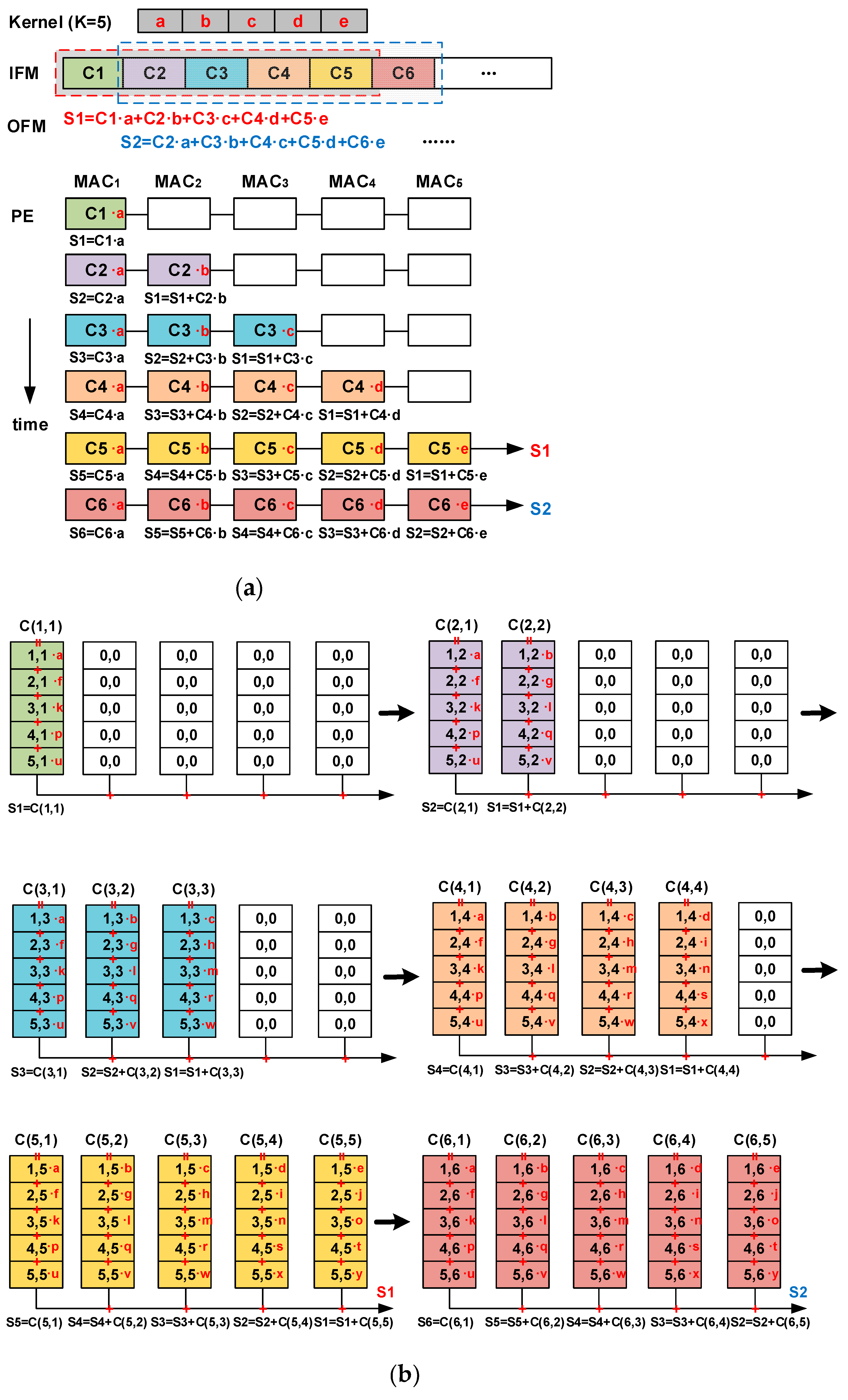
In
Figure 5a, consider a scenario with a one-dimensional (1-D) IFM. A 1-D convolution kernel, five units long, moves across the IFM with a stride of one unit. According to (1), the resulting 1-D OFM consists of segments such as
S1,
S2,
S3, and so on. The 1-D PE is constructed from a chain of MACs, each extending the length of K. The convolution operation in this setup is effectively executed within a 1-D PE by employing the CB dataflow. Algorithm 1 describes this progress.
| Algorithm 1 One-dimensional column-buffering dataflow. |
Input: The size of the kernel K. The size of the IFM L. The size of the OFM C. The sequence of the partial IFM i. The sequence of the partial OFM n. The ith partial IFM Ci.
Output: The ith partial OFM.
Initiate: i = n = 1, Sn = 0
1: for i = 1, 2, 3, …, L do
2: MACj = Ci, j∈[1, min(i, K)]
3: Sn = Sn + Ci ×Wi−n+1, n∈[max(1, i − k + 1), i]
4: if i − n + 1 = K then
5: output Si
6: end if
7: end for |
In a two-dimensional (2-D) PE, the CB dataflow scenario is essentially an expansion of the 1-D case. For the IFM, data are arranged in columns extending across
K rows, with the weights fixed in sequence within the PE. This arrangement converts the partial sum
S into an accumulated sum of the products of each IFM data column
C with their corresponding weights. As shown in
Figure 5b, the specific steps are as follows:
The first column of IFM data, C1, enters the first column of MACs, marked as C(1,1). It multiplies with the weights of the first column, and the results are summed to form the first intermediate result, S1;
The second column of IFM data, C2, enters both the first and second columns of MACs, marked as C(2,1) and C(2,2). After multiplication with the first and second column weights and subsequent summation, the second intermediate result, S2, is obtained. S2 is then added to the previously accumulated intermediate result, S1;
Continuing with this pattern, the third and fourth columns of data are processed, yielding intermediate results from S1 to S4;
The fifth column of IFM data, C5, is processed by the MACs from the first to the fifth columns. Post multiplication with the corresponding column weights and summation, the intermediate results from S1 to S5 are derived. As S1 has now been accumulated five times, it completes the first part of the OFM sum and is outputted from the PE;
For the sixth column of IFM data, C6, a similar process occurs across the first to fifth column MACs, marked as C(6,1) to C(6,5), resulting in intermediate results from S2 to S6. Subsequently, S2, following S1, is also outputted from the PE.
5. System Architecture
5.1. Overview
To boost the computational speed and efficiency of neural networks, hardware acceleration has been implemented. The architecture features specialized modules for weight and data storage, ensuring rapid access to and processing of data, which further improves efficiency. The proposed bit-serial CNN accelerator’s system architecture, illustrated in
Figure 6, is centered around two key PEA computation modules: one for convolutional layers, named the CL PEA, and another for fully connected layers, called the FCL PEA. The CL PEA consists of six PEs which include one-hundred fifty MACs and six adder trees, while the FCL PEA is made up of twenty-five MACs and an adder tree.
Other critical components include three random access memories (RAMs) housing IFMs, OFMs, and weights, along with their corresponding buffers, a pooling module, and a top-level control unit. The BUS facilitates data transfer between the system and external storage units. The TOP_CON unit controls the flow of data and addresses. The Con_flag, a control flag with a bit width of only 1 bit, indicates the start or end of both external and internal data transfers. Multiple address lines in the Address component locate data within RAMs, with the bit width of the addresses depending on the amount of data stored in the RAM—the more data stored, the wider the corresponding Address. DATA is the primary data transmission line, and DATA_BUF serves as a buffering unit. Data flows from the BUS into the RAM, buffers through DATA_BUF, and is then directed to either the CL PEA, FCL PEA, or the POOL module. Before entering DATA_BUF, DATA is in a parallel format with a bit width of 8 bits. However, due to parallel-to-serial conversion circuits within DATA_BUF, DATA can be converted to either 30 or 25 serial data streams for simultaneous input, according to the requirements of the CL PEA or FCL PEA. The diagram includes six RAMs for storing data, with WEIGHT_RAM specifically designated for weight data. RAMs store data either in parallel or after undergoing a serial-to-parallel conversion. After passing through the internal DATA_BUF and transitioning from 8 bits to 1 bit, the Weight line transfers weight data from WEIGHT_RAM to the CL PEA or FCL PEA. Lastly, the POOL module conducts pooling operations, a standard practice in CNNs that effectively compresses data size.
Upon system startup, the
TOP_CON unit takes the lead in initializing and configuring all modules. Data are then loaded into the RAM and
WEIGHT_RAM via the
BUS. During neural network forward propagation, data and weights are routed to the CL PEA for computation. In this process, each PE unit handles data in parallel, executing multiply–accumulate operations. The computed intermediate results are first temporarily stored in
DATA_BUF. They then undergo quantization and ReLU function processing before being stored back in the RAM. The processed data are later read out and subjected to pooling operations in the
POOL module, as illustrated by the red dashed line in
Figure 6, which traces the data movement pathway for the first CL. Finally, the data, after being processed by the second pooling layer, are internally transferred to the RAM designated for the FCL using the
DATA line. Then, the FCL PEA processes the data matrix. The output of the last FCL is then conveyed out of the system through the
BUS, following the path shown by the blue dashed line in
Figure 6. This line maps out the data movement trajectory post-second CL and through the three layers of the FCL.
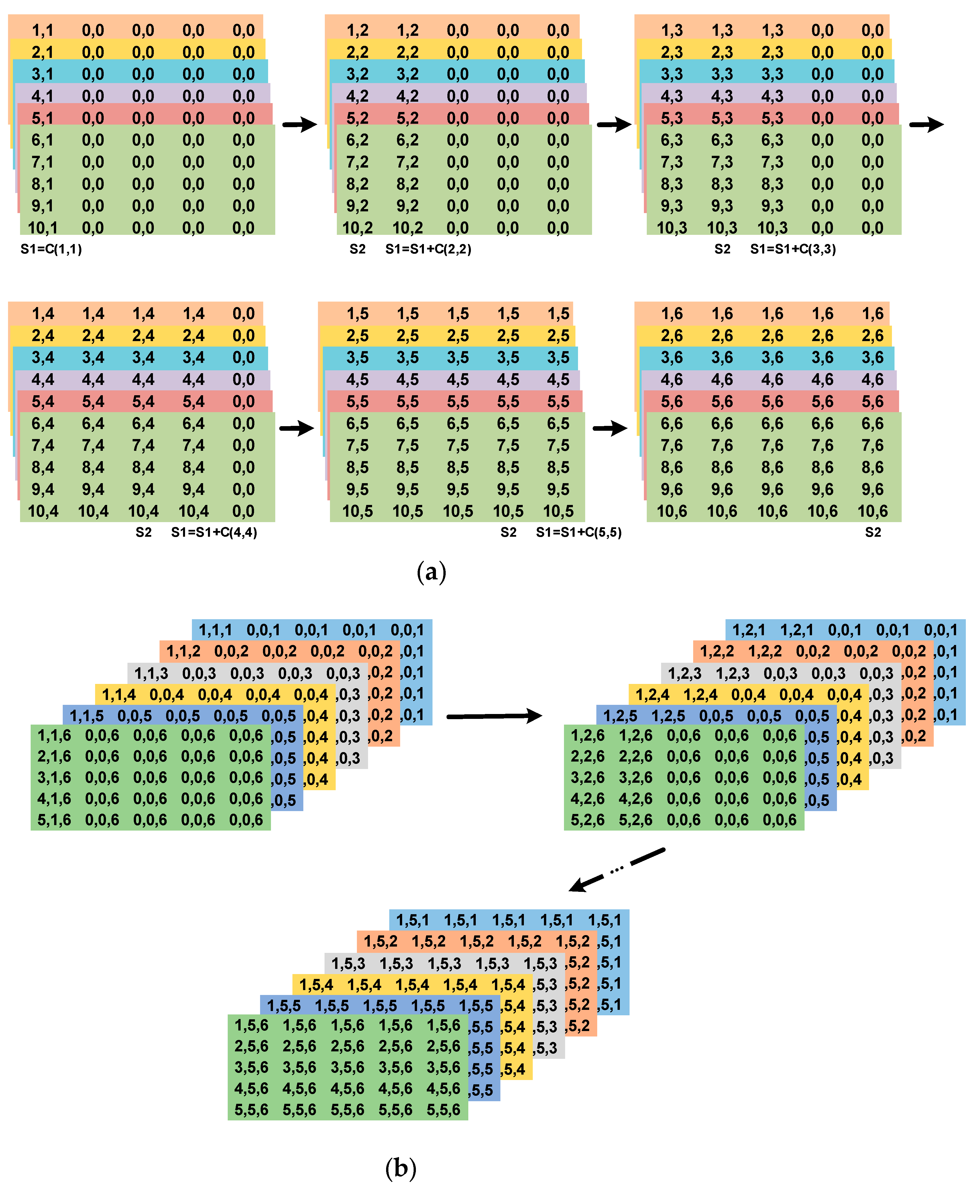
5.2. Design of the PEA
The architecture of the PEA is shown in
Figure 7a, comprising six PEs. Each PE consists of MACs for multiplication and a
TREE structure for summing the multiplication outputs. The input IFM data are segmented into columns of
K × 1 and updated in a zigzag pattern across columns, beginning with the first one. This processing, which involves several MACs, is elaborated in
Section 4, which focuses on the CB dataflow. At the base of each PE, there are multiple
TREE structures. These are designed to consolidate data from the MACs and relay the combined output to the subsequent processing phase. In our work, as the multipliers operate in a serial fashion, data throughout the PE are transferred serially. This approach effectively reduces the data width and simplifies the interface connections, a concept further expounded in
Section 5.3. The adder tree adopts a structure of pairwise addition, with its registers (REGs) serving as cascading interfaces.
In the computation of CLs, if we input five pixels from the IFM simultaneously, it takes five clock cycles. With a parallel multiplier architecture, an 8-bit data computation in such a setup requires only one clock cycle. This scenario results in the data input time being significantly longer than the data computation time, with a notable difference of four clock cycles. This observation leads us to explore ways to align the data computation time more closely with the data input time or at least reduce this time discrepancy.
Using a serial multiplier architecture, the computation of 8-bit data takes eight clock cycles, which means the computation time now exceeds the data input time. However, this change reduces the gap between computation and input times to three clock cycles, achieving better synchronization between the two. If we could further extend the data input time, the disparity between the computation time and data input time could be decreased even more. With these considerations in mind, particularly for the LeNet-5 model, we have a specific dataflow format for each CL, as shown in
Figure 8.
The first CL features six convolution kernels, each measuring 5 × 5. When inputting only five pixels from the IFM at a time, the process takes five clock cycles, fewer than the eight cycles required for computation. Processing with six different convolution kernels simultaneously still results in a duration of five clock cycles, which does not effectively extend the data input time. To address this, we shifted our focus from processing across the depth of the convolution kernels to a vertical approach, simultaneously convolving multiple rows of the same convolution kernel. When using six identical convolution kernels at once to expedite processing in the same layer, we need to input ten IFM pixels. This approach allows the bit-serial computation speed to outpace the data reading speed. In comparison to parallel computation, both structures primarily contend with the challenge of slow data reading speeds rather than an inherent slow computation speed in serial configurations. Under these conditions, the unique benefits of the serial structure—its compact size and lower power consumption—come to the forefront. For the first CL, which convolves six identical kernels simultaneously, each kernel processes different data but shares the same weights. The PE requires 150 MACs to complete six convolution rounds. Therefore, the PEA for the first layer comprises six PE layers, with each PE layer equipped with six adder trees.
In the second CL, there are 16 convolution kernels, each with a depth of six. Each of these kernels handles different data and operates with unique weights. Consequently, in this layer, only one convolution kernel is active at a time, completing a total of 16 convolution cycles. The PE configuration remains the same, requiring 150 MACs, thereby facilitating the reuse of the MACs. The PEA for the second layer also comprises six PE layers, and each of these layers is outfitted with six adder trees. Additionally, a larger TREE structure is employed to aggregate the outputs from these adder trees. The data processed through this layer are then serialized and outputted using a bit-serial output approach.
In the computations for FCLs, which essentially execute matrix multiplication similar to 1 × 1 convolution operations, there is no data reuse. As a result, the CL PEA, optimized for data reuse in convolutional processes, is not applicable to FCLs. This necessitates the use of a dedicated PEA specifically for the FCL computations. We segmented the network into two parts: one comprising convolution and pooling and another dedicated to fully connected operations, effectively creating a single-level pipeline. Theoretically, after calculating the time required for both convolution and pooling, the FCLs employ 25 MACs for their computations. With these 25 MACs in action, the total processing time for the three FCLs is actually less than the time needed for both convolution and pooling. Hence, the FCL PEA operates by calculating the products of 25 IFMs and their corresponding weights, storing these intermediate data and subsequently summing up multiple sets of intermediate data to arrive at a final result.
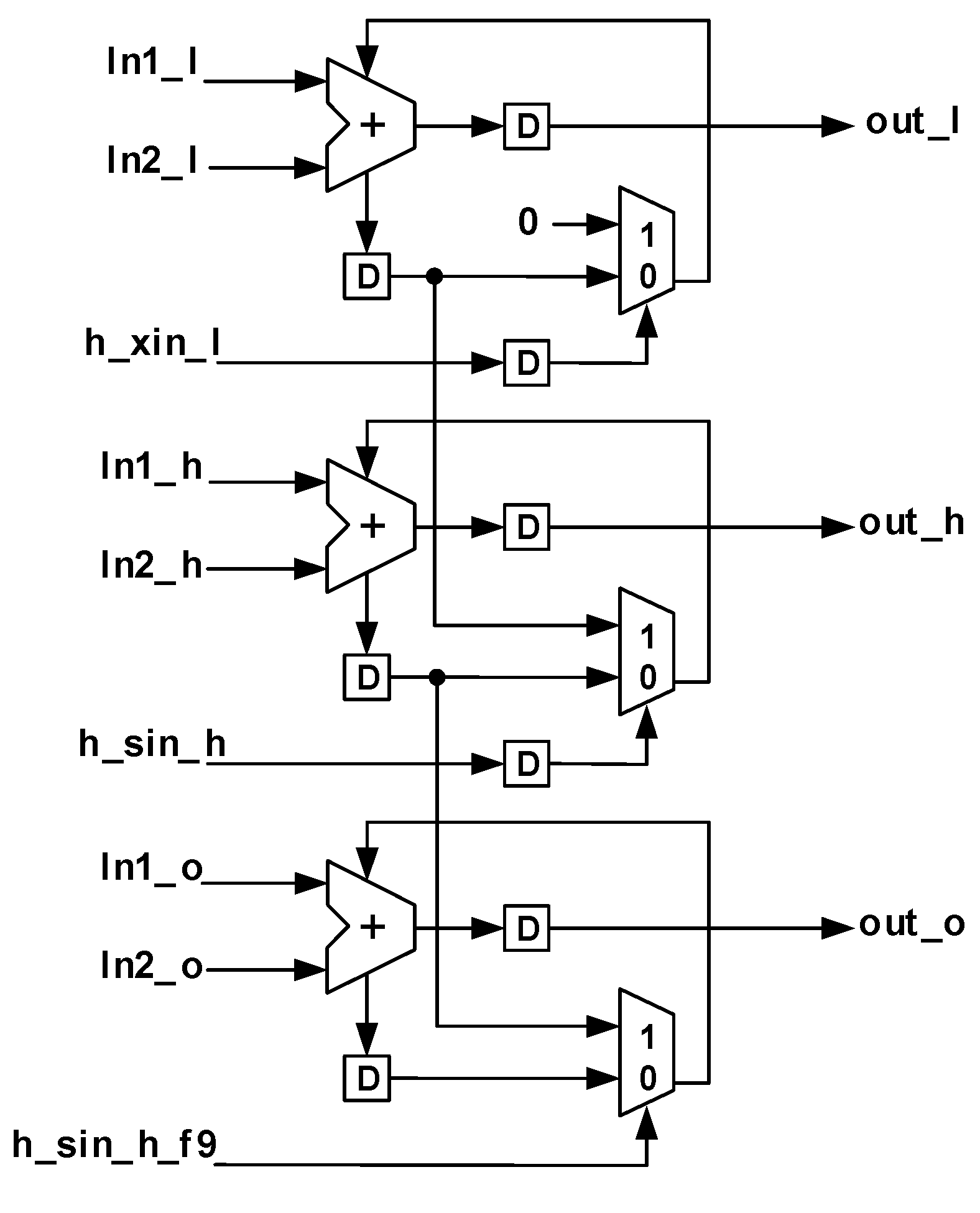
5.3. The Design of the MAC
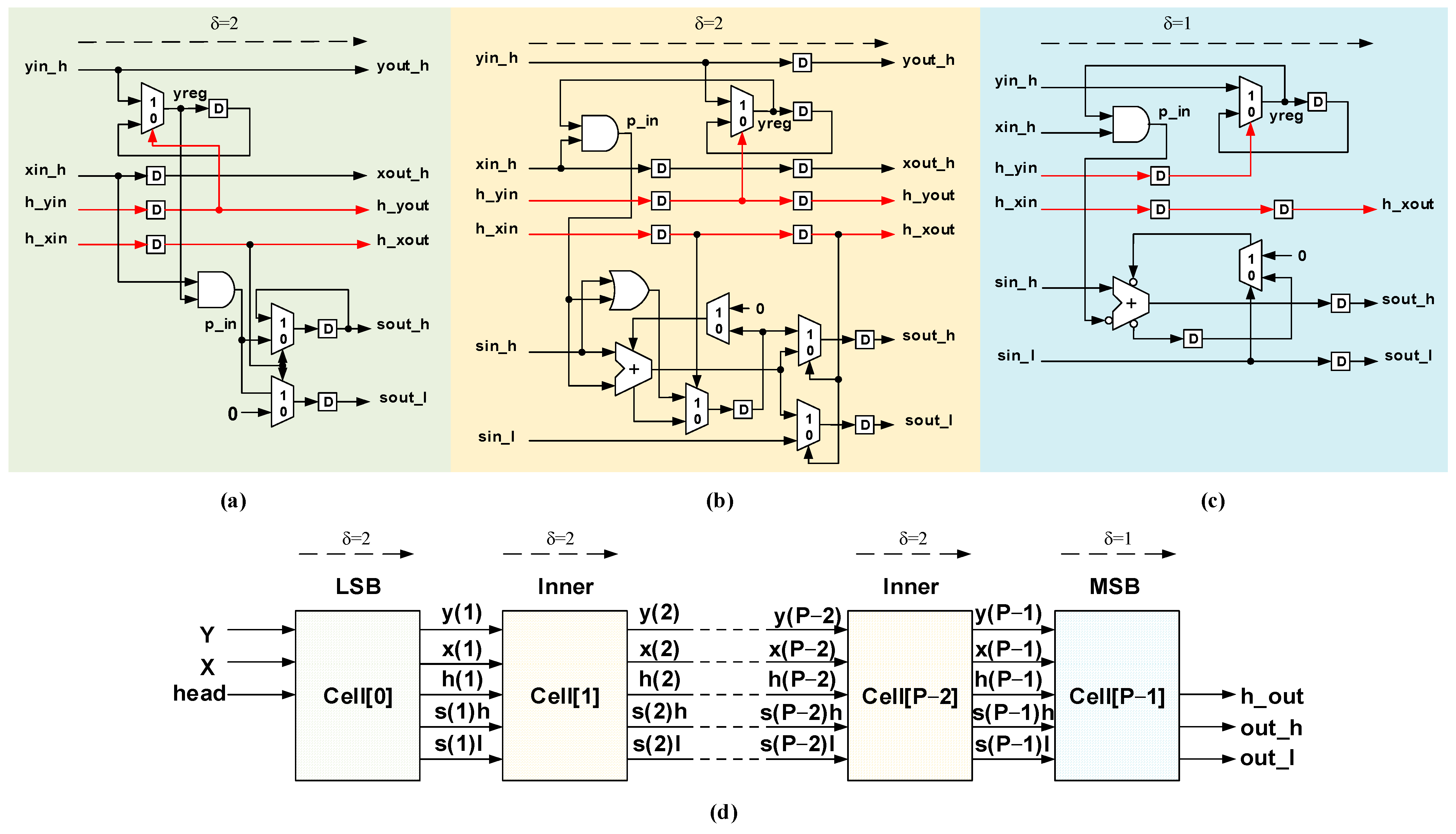
Leveraging the benefits of low power usage, compact size, and high operational frequency, we adapted the multiplier design from Isshiki [
32] to reduce the count of serial–parallel and parallel–serial conversion circuits. This adaptation involves splitting the input head bit signals into two distinct components,
h_yin and
h_xin, as showcased by the red-highlighted circuit in
Figure 9. This split is designed to individually represent the head bit signals for the input IFM and weights. By doing so, it aligns with the principles of the WS dataflow or CB dataflow, enabling the weights to remain fixed within the circuit, thus eliminating the need for constant memory access for inputs. Consequently, this modification not only keeps the number of serial–parallel and parallel–serial conversion circuits for the IFM at 30 but also efficiently maintains the serial–parallel and parallel–serial conversion circuits for the weights at 30 rather than increasing them to 150.
On hardware platforms, to streamline the quantization of accumulated tensors and align with the norms of hardware quantization, it is advantageous for the quantization scale to be a power of two instead of using dividers, which need huge hardware resources. This strategy allows for the use of simple data right-shifting to replace complex and resource-intensive division operations. With the goal of minimizing the storage size for intermediate data and conserving hardware resources, and after considering the range of data sizes and the number of accumulations involved, we transitioned from the standard 32-bit intermediate data size to a 24-bit format. This modification was intended to manage the impact of data overflow effectively. The design of the corresponding adder, as depicted in
Figure 10, reflects this change. We utilized the 23rd bit, i.e., the MSB, as the sign bit, combined with bits 14 to 8, to construct the hardware-quantized number, and discarded the rest. This approach needs to ensure that the reconfigured data remain within the INT8 data range.
6. Implementation and Evaluation
To implement and assess our LeNet-5 accelerator design, we employed two approaches. On the software side, we used the MNIST dataset for training. After quantization, we exported the IFM and weights to the hardware. For the hardware aspect, we utilized Verilog for implementation and conducted simulations with Synopsys VCS and Verdi. These simulations allowed us to gauge the neural network’s performance when it processed complete images for inference. Moreover, we synthesized the design under the TSMC 40 nm process using Design Compiler. This process helped us gather vital data regarding the design’s area, power consumption, gate count, and so on. Furthermore, we leveraged a field-programmable gate array (FPGA) board, specifically the model XC7K325TFFG900-2, for comprehensive functional verification of the entire accelerator. This step was crucial in gaining parameters like FPGA capability and running time.
6.1. CNN Validation
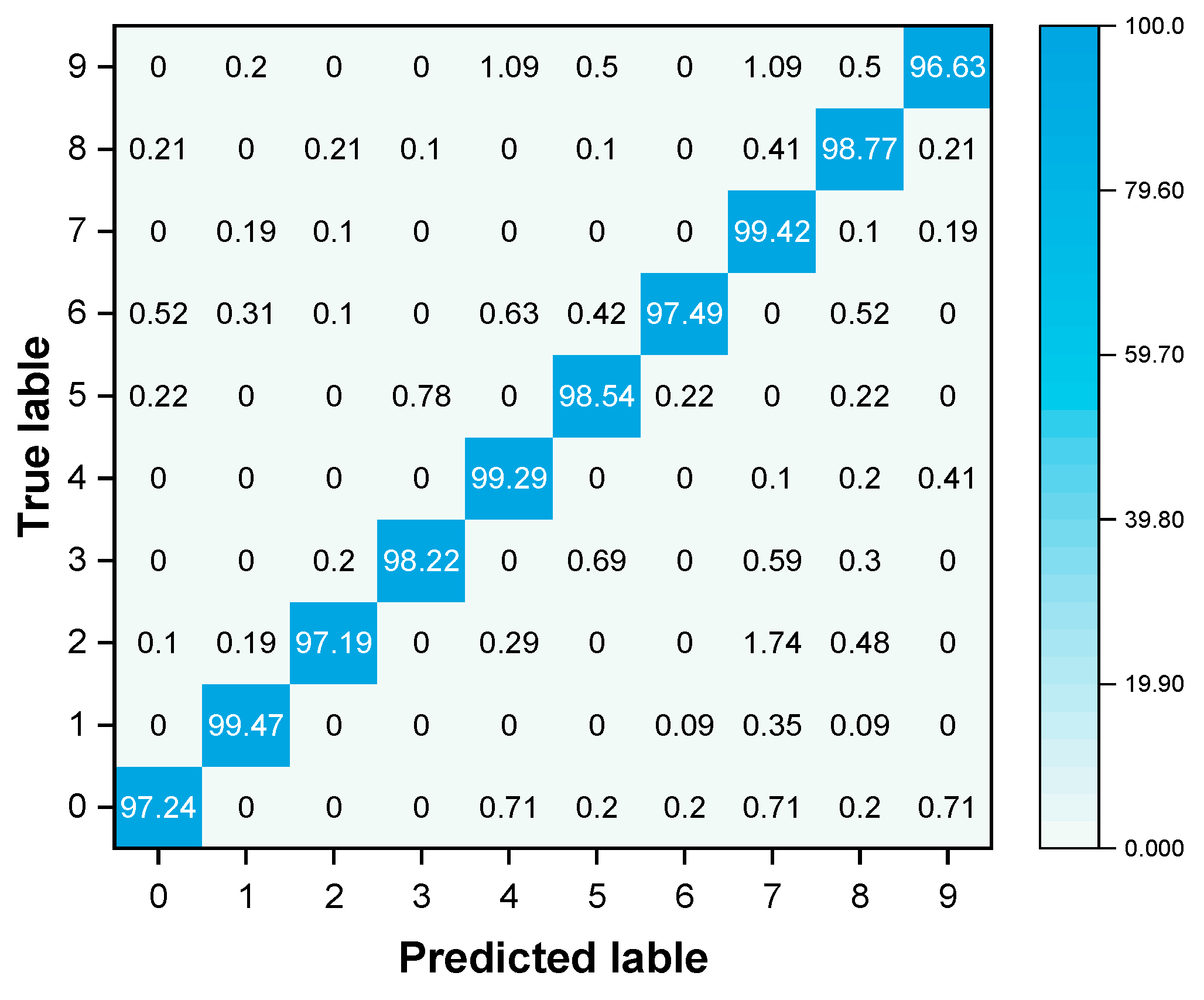
A confusion matrix is an essential tool for assessing the performance of classification models, particularly in tasks like image recognition. It is structured such that each row corresponds to a true label, while each column aligns with a label predicted by the model. An analysis of
Figure 11 reveals that the diagonal numbers indicate the proportion of correctly classified instances. In this matrix, high values along the diagonal suggest that our model accurately classifies the MNIST handwritten digit dataset in most instances. Values off the diagonal highlight labels for which the model becomes confused, indicating a mismatch between true and predicted labels. The model’s performance is inversely proportional to these values. In the matrix, most non-diagonal values are notably low, pointing to minimal classification errors. A closer look reveals that the number 1 is less likely to be confused with other numbers, as indicated by the near-zero values in its row, except for the diagonal. The number 9 has a slightly lower correct recognition rate, likely due to its visual resemblance to the numbers 4 and 7, causing some confusion. Similar shapes might also lead to confusion between numbers like 4 and 9 or 3 and 5. In conclusion, this confusion matrix demonstrates the high efficacy of our LeNet-5 accelerator in the MNIST handwritten digit recognition task. With an impressive accuracy rate of 98.24%, it shows only some confusion, underscoring the model’s robustness in accurately classifying digits.
6.2. Synthesis Results
In
Table 2, it is evident that this project stands out among other ASIC LeNet-5 implementations, especially with its operation at a frequency of 500 MHz using TSMC 40 nm technology. This frequency surpasses that of most listed projects. Furthermore, the chip’s compact footprint, at just 0.41 mm
2 with a gate count of 50,000, is notably smaller than its counterparts. For a fair comparison, the normalized area is given, and it is still smaller than others. The power consumption is impressively low at 91.84 mW, a considerable reduction from the third-lowest reported figure of 297 mW. However, this work’s normalized power consumption value at 40 nm and a 1.0 V CMOS process is minimal in comparison. The normalized hardware efficiency rate of 0.1574 MOPS/Gate is competitive within the context of the works presented. Moreover, our project boasts the integration of 369 kB of on-chip SRAM, which exceeds the amount found in many other studies. While the parallel version [
34] boasts a classification accuracy of 98.80%, our work, which supports FCL and operates with just half of the data bit width, achieves a nearly equivalent accuracy of 98.28%. This highlights our design’s capability to balance high accuracy with efficient hardware and area utilization, particularly under the constraints of limited hardware resources. Overall, our work demonstrates considerable potential for practical applications, particularly in environments in which resources are constrained, such as mobile and edge computing devices.
6.3. Prototype Verification
To validate the bit-serial LeNet-5 accelerator proposed in our research, we conducted prototype testing using an FPGA. The resource utilization for this FPGA implementation is detailed in
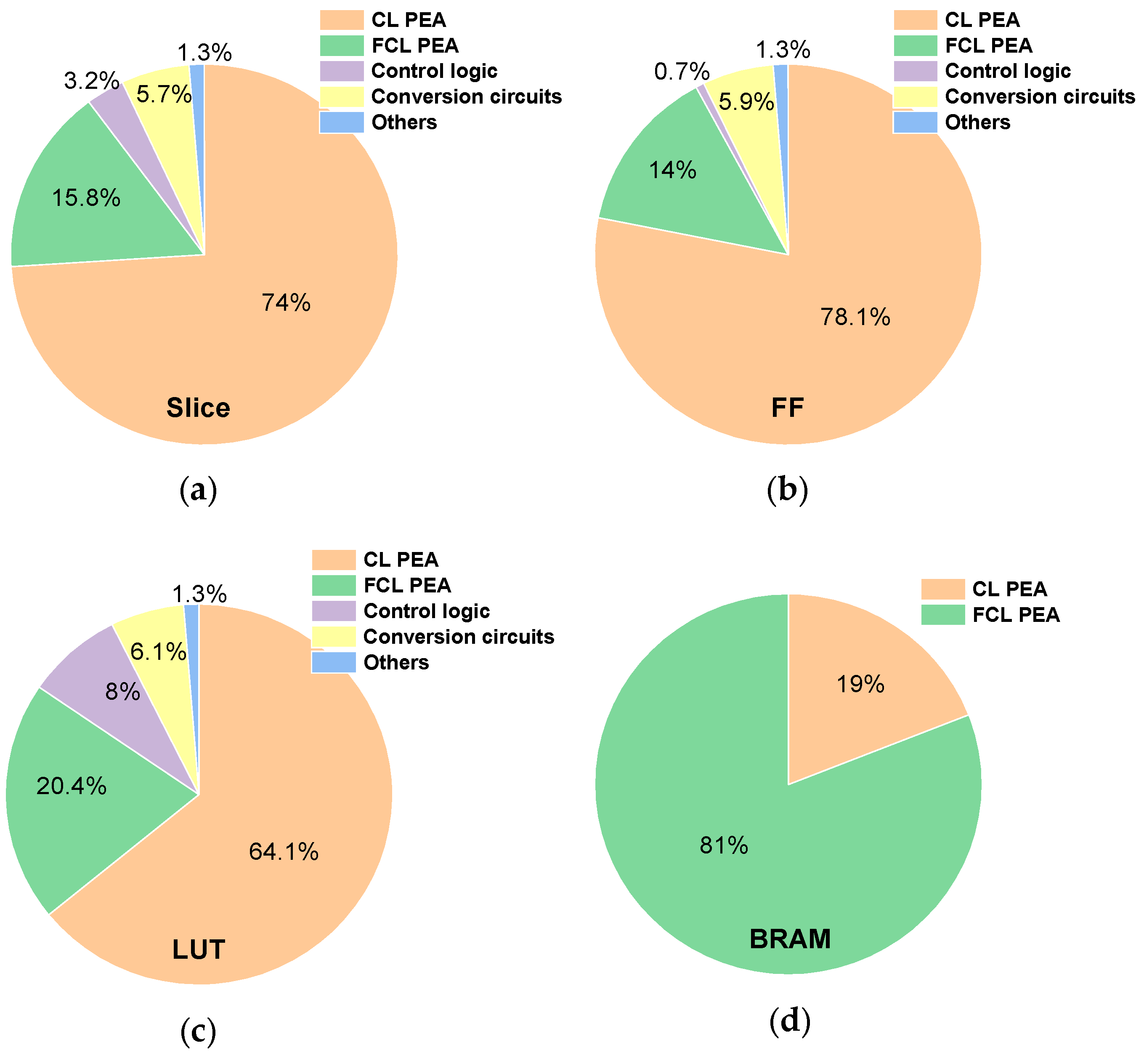
Table 3. On the Xilinx Kintex-7 FPGA, we achieved a notably high operating frequency of 500 MHz. Obviously, the Digital Signal Processor (DSP) utilization is exceptionally low at just 0.24%. This is primarily due to the control logic used in the CNN accelerator, and in theory, the DSP count should be zero. The utilization of Slices, which are fundamental for implementing logic functions, stands at 4.21%. This rate indicates a moderate consumption of the FPGA’s logic resources by our design. Flip-flops (FFs) show a utilization rate of 4.67%. This metric usually signifies the quantity of registers in use. The Look-Up Table (LUT) utilization, crucial for executing combinational logic, is at 4.41%. This illustrates the extent of combinational logic resource occupation. Additionally, the block RAM (BRAM) utilization is just 4.72%. This balanced approach to resource usage across different components suggests that our design efficiently leverages available FPGA resources without over-reliance on any single type. This balance not only indicates a well-optimized design but also suggests that our design is relatively simpler in complexity when compared to other similar designs.
Figure 12 showcases the distribution of FPGA resources among the various components of the bit-serial LeNet-5 accelerator. The breakdown for Slices, FFs, and LUTs is detailed in
Figure 12a–c. Notably, the CL is more computation-intensive, while the FCL demands more storage. Consequently, the PEA for the CL occupies the most significant portion, followed by the FCL PEA and then the serial–parallel and parallel–serial conversion circuits. When it comes to BRAM utilization, the BRAM share of the CL PEA is smaller than that of the FCL PEA, reflecting the different resource demands of these layers.
Table 4 outlines the throughput and performance metrics for each layer of LeNet-5 when implemented on an FPGA, operating at a 500 MHz frequency. The convolutional layers CL1 and CL2 have processing times of 19.20 μs and 134.40 μs, respectively, with CL1 exhibiting a remarkable performance of 12.49 GOPS and CL2 at 7.02 GOPS. The fully connected layers, FCL1, FCL2, and FCL3, take 96.00 μs, 20.16 μs, and 1.68 μs, respectively, to process, each achieving a performance of 1.00 GOPS. The pooling layers, POOL1 and POOL2, have processing times of 9.44 μs and 3.24 μs, respectively. These layers exhibit lower performance compared to the convolutional layers, with outputs of 0.50 GOPS and 0.49 GOPS. The pooling layers emerge as the primary bottleneck as the CLs and FCLs form a first-level pipeline, necessitating a wait time during computation. Overall, with the pipeline structure, the entire LeNet-5 framework achieves an average processing time of 166.28 μs excluding the FCLs’ time, a total computational demand of 1308.19 KOP, and an impressive average performance of 7.87 GOPS. These data indicate that the FPGA demonstrates higher efficiency in the convolutional layers and comparatively lower efficiency in the pooling layers.
Table 5 presents a comparative analysis of the LeNet-5 model’s performance across various works. This study differentiates itself from two other studies, Refs. [
37,
38], by employing a bit-serial processing approach, in contrast to their parallel methodologies. In terms of accuracy, our study achieves an impressive 98.24%, slightly surpassing [
38], but falls marginally short of [
37]’s 98.60%. Precision-wise, both our study and [
37] utilize 8-bit fixed precision computing, while [
38] opts for 16-bit. Focusing on the FCL support, both our study and [
37] include it, unlike [
38]. Frequency tests reveal that our FPGA operates at a swift 500 MHz, significantly exceeding the 136 MHz of [
37] and the 88.07 MHz of [
38]. When it comes to resource utilization efficiency, our study shows a marked advantage in DSP, LUT, FF and BRAM, indicating superior resource efficiency compared to [
37]. Although our power consumption stands at 865 W, slightly higher than [
38]’s 616 W, we notably excel in throughput (7.87 GOPS) and energy efficiency (9.10 GOPS/W). Our processing time is a rapid 284.13 μs, vastly outpacing the 4530 μs of [
37] and 734 μs of [
38]. In summary, despite a marginally higher power consumption compared to [
38], our work demonstrates outstanding performance in terms of accuracy, throughput, energy efficiency, and processing speed.
Finally, we uploaded our LeNet-5 accelerator onto the FPGA. For the test data, the quantized weights and feature map parameters were converted into binary format. These binary data were then compiled into COE (coefficient) files, which were integrated into the RAMs of the accelerator. This integration was crucial as utilizing COE files for parameter transmission is a common practice in accelerator configurations. COE files are structured in ASCII text format, with the header specifying a radix of 2, indicating that the data were represented in binary. Data within these files were organized in vector format, with each vector ending in a semicolon and vectors separated by commas. During this phase, the Vivado tool interpreted the COE file format and generated corresponding Memory Initialization File (MIF) format files. These MIF files were then employed in behavioral-level simulations to verify the system’s accuracy and functionality.
Our FPGA board, however, was equipped with only eight LEDs, which is insufficient for fully representing ten labels of digits. As a workaround, we implemented a five-digit binary encoding system. Take the number 6, for instance, which corresponds to the seventh label. This would be represented as 00111 in our system. Considering that the LEDs are activated at a low level and the MSB is positioned on the right, this results in the rightmost two LEDs lighting up while the next three remain off. The leftmost three LEDs serve to indicate the predicted number’s position. In this setup, an unlit middle LED signifies the correct positioning of the predicted number, coded as 010. Therefore, for a correctly predicted number 6, the final output displayed would be 01011100, as depicted in
Figure 13. This demonstration effectively validates the functional accuracy of our work.
7. Conclusions
In our study, we explored a bit-serial neural network accelerator, aiming to tackle the challenges of size, power consumption, and hardware efficiency often found in traditional neural network accelerators. Our paper presents an approach that integrates a bit-serial MAC, advanced dataflow techniques, and architectural optimizations. At its core is the column-buffering dataflow technique, which dramatically reduces the need for accessing and moving intermediate feature maps, thereby boosting efficiency. Moreover, we implemented an enhanced quantization process that effectively eliminates bias, streamlining the computation process. The paper meticulously outlines the design of a LeNet-5 accelerator centered around a convolutional layer processing element array and featuring an improved bit-serial multiply–accumulate unit. The experimental results are impressive, demonstrating that our design surpasses the current state-of-the-art ASIC designs in frequency, chip area, and power consumption. A standout feature of our design is its ability to deliver high performance, i.e., achieve a 7.87 GOPS on a Xilinx Kintex-7 FPGA, while using fewer hardware resources and maintaining a brief processing time of 284.13 μs. These outcomes highlight the design’s suitability for applications that demand compact and energy-efficient solutions.
Author Contributions
Conceptualization, all authors; methodology, X.C. and Y.W.; software and validation, X.C., W.D. and H.L.; formal analysis, X.C. and Y.W.; investigation, X.C.; resources, Y.W. and P.L.; data curation, X.C., W.D. and H.L.; writing—original draft preparation, X.C., W.D. and H.L.; writing—review and editing, all authors; visualization, X.C., W.D. and H.L.; supervision, Y.W. and P.L.; project administration, X.C., W.D. and H.L.; funding acquisition, Y.W. and P.L. All authors have read and agreed to the published version of the manuscript.
Funding
This research received no external funding.
Institutional Review Board Statement
Not applicable.
Informed Consent Statement
Not applicable.
Data Availability Statement
All data underlying the results are available as part of the article and no additional source data are required.
Acknowledgments
This work was supported by the State Key Laboratory of Electronic Thin Films and Integrated Devices.
Conflicts of Interest
The authors declare no conflicts of interest.
References
- Hsu, L.-C.; Chiu, C.-T.; Lin, K.-T.; Chou, H.-H.; Pu, Y.-Y. ESSA: An Energy-Aware Bit-Serial Streaming Deep Convolutional Neural Network Accelerator. J. Syst. Archit. 2020, 111, 10183. [Google Scholar] [CrossRef]
- Lee, J.; Kim, C.; Kang, S.; Shin, D.; Kim, S.; Yoo, H.-J. UNPU: An Energy-Efficient Deep Neural Network Accelerator with Fully Variable Weight Bit Precision. IEEE J. Solid-State Circuits 2019, 54, 173–185. [Google Scholar] [CrossRef]
- Judd, P.; Albericio, J.; Hetherington, T.; Aamodt, T.M.; Moshovos, A. Stripes: Bit-Serial Deep Neural Network Computing. In Proceedings of the 2016 49th Annual IEEE/ACM International Symposium on Microarchitecture (MICRO), Taipei, Taiwan, 15–19 October 2016; IEEE: Taipei, Taiwan, 2016; pp. 1–12. [Google Scholar]
- Chen, T.; Du, Z.; Sun, N. DianNao: A Small-Footprint High-Throughput Accelerator for Ubiquitous Machine-Learning. ACM SIGARCH Comput. Archit. News 2014, 42, 269–284. [Google Scholar] [CrossRef]
- Ma, M.; Tan, J.; Wei, X.; Yan, K. Process Variation Mitigation on Convolutional Neural Network Accelerator Architecture. In Proceedings of the 2019 IEEE 37th International Conference on Computer Design (ICCD), Abu Dhabi, United Arab Emirates, 17–20 November 2019; pp. 47–55. [Google Scholar]
- Lee, H.; Wu, Y.-H.; Lin, Y.-S.; Chien, S.-Y. Convolutional Neural Network Accelerator with Vector Quantization. In Proceedings of the 2019 IEEE International Symposium on Circuits and Systems (ISCAS), Sapporo, Japan, 26–29 May 2019; pp. 1–5. [Google Scholar]
- Sze, V.; Chen, Y.-H.; Yang, T.-J.; Emer, J.S. Efficient Processing of Deep Neural Networks: A Tutorial and Survey. Proc. IEEE 2017, 105, 2295–2329. [Google Scholar] [CrossRef]
- Chen, Y.-H.; Emer, J.; Sze, V. Eyeriss: A Spatial Architecture for Energy-Efficient Dataflow for Convolutional Neural Networks. ACM SIGARCH Comput. Archit. News 2016, 44, 367–379. [Google Scholar] [CrossRef]
- Chen, Y.; Luo, T.; Liu, S.; Zhang, S.; He, L.; Wang, J.; Li, L.; Chen, T.; Xu, Z.; Sun, N.; et al. DaDianNao: A Machine-Learning Supercomputer. In Proceedings of the 2014 47th Annual IEEE/ACM International Symposium on Microarchitecture, Cambridge, UK, 13–17 December 2014; IEEE: Cambridge, UK; pp. 609–622. [Google Scholar]
- Parashar, A.; Rhu, M.; Mukkara, A.; Puglielli, A.; Venkatesan, R.; Khailany, B.; Emer, J.; Keckler, S.W.; Dally, W.J. SCNN: An Accelerator for Compressed-Sparse Convolutional Neural Networks. ACM SIGARCH Comput. Archit. News 2017, 45, 27–40. [Google Scholar] [CrossRef]
- Kim, M.; Seo, J.-S. Deep Convolutional Neural Network Accelerator Featuring Conditional Computing and Low External Memory Access. In Proceedings of the 2020 IEEE Custom Integrated Circuits Conference (CICC), Boston, MA, USA, 22–25 March 2020; pp. 1–4. [Google Scholar]
- Zheng, Y.; Yang, H.; Shu, Y.; Jia, Y.; Huang, Z. Optimizing Off-Chip Memory Access for Deep Neural Network Accelerator. IEEE Trans. Circuits Syst. II Express Briefs 2022, 69, 2316–2320. [Google Scholar] [CrossRef]
- Jia, H.; Ren, D.; Zou, X. An FPGA-Based Accelerator for Deep Neural Network with Novel Reconfigurable Architecture. IEICE Electron. Express 2021, 18, 20210012. [Google Scholar] [CrossRef]
- Choi, Y.; Bae, D.; Sim, J.; Choi, S.; Kim, M.; Kim, L.-S. Energy-Efficient Design of Processing Element for Convolutional Neural Network. IEEE Trans. Circuits Syst. II Express Briefs 2017, 64, 1332–1336. [Google Scholar] [CrossRef]
- Peemen, M.; Setio, A.A.A.; Mesman, B.; Corporaal, H. Memory-Centric Accelerator Design for Convolutional Neural Networks. In Proceedings of the 2013 IEEE 31st International Conference on Computer Design (ICCD), Asheville, NC, USA, 6–9 October 2013; pp. 13–19. [Google Scholar]
- Zhang, C.; Li, P.; Sun, G.; Guan, Y.; Xiao, B.; Cong, J. Optimizing FPGA-Based Accelerator Design for Deep Convolutional Neural Networks. In Proceedings of the 2015 ACM/SIGDA International Symposium on Field-Programmable Gate Arrays—FPGA ’15, Monterey, CA, USA, 22–24 February 2015; pp. 161–170. [Google Scholar]
- Kulkarni, A.; Abtahi, T.; Shea, C.; Kulkarni, A.; Mohsenin, T. PACENet: Energy Efficient Acceleration for Convolutional Network on Embedded Platform. In Proceedings of the 2017 IEEE International Symposium on Circuits and Systems (ISCAS), Baltimore, MD, USA, 28–31 May 2017; pp. 1–4. [Google Scholar]
- Moons, B.; Uytterhoeven, R.; Dehaene, W.; Verhelst, M. Envision: A 0.26-to-10TOPS/W Subword-Parallel Dynamic-Voltage-Accuracy-Frequency-Scalable Convolutional Neural Network Processor in 28 nm FDSOI. In Proceedings of the 2017 IEEE International Solid-State Circuits Conference (ISSCC), San Francisco, CA, USA, 5–9 February 2017; pp. 246–247. [Google Scholar]
- Desoli, G.; Chawla, N.; Boesch, T.; Singh, S.; Guidetti, E.; De Ambroggi, F.; Majo, T.; Zambotti, P.; Ayodhyawasi, M.; Singh, H.; et al. A 2.9TOPS/W Deep Convolutional Neural Network SoC in FD-SOI 28 nm for Intelligent Embedded Systems. In Proceedings of the 2017 IEEE International Solid-State Circuits Conference (ISSCC), San Francisco, CA, USA, 5–9 February 2017; pp. 238–239. [Google Scholar]
- Bai, L.; Zhao, Y.; Huang, X. A CNN Accelerator on FPGA Using Depthwise Separable Convolution. IEEE Trans. Circuits Syst. II Express Briefs 2018, 65, 1415–1419. [Google Scholar] [CrossRef]
- Jo, J.; Cha, S.; Rho, D.; Park, I.-C. DSIP: A Scalable Inference Accelerator for Convolutional Neural Networks. IEEE J. Solid-State Circuits 2018, 53, 605–618. [Google Scholar] [CrossRef]
- Ding, W.; Huang, Z.; Huang, Z.; Tian, L.; Wang, H.; Feng, S. Designing Efficient Accelerator of Depthwise Separable Convolutional Neural Network on FPGA. J. Syst. Archit. 2019, 97, 278–286. [Google Scholar] [CrossRef]
- Farahani, A.; Beithollahi, H.; Fathi, M.; Barangi, R. CNNX: A Low Cost, CNN Accelerator for Embedded System in Vision at Edge. Arab. J. Sci. Eng. 2023, 48, 1537–1545. [Google Scholar] [CrossRef]
- Li, H.; Fan, X.; Jiao, L.; Cao, W.; Zhou, X.; Wang, L. A High Performance FPGA-Based Accelerator for Large-Scale Convolutional Neural Networks. In Proceedings of the 2016 26th International Conference on Field Programmable Logic and Applications (FPL), Lausanne, Switzerland, 29 August–2 September 2016; pp. 1–9. [Google Scholar]
- Zhou, X.; Zhang, L.; Guo, C.; Yin, X.; Zhuo, C. A Convolutional Neural Network Accelerator Architecture with Fine-Granular Mixed Precision Configurability. In Proceedings of the 2020 IEEE International Symposium on Circuits and Systems (ISCAS), Seville, Spain, 12–14 October 2020; pp. 1–5. [Google Scholar]
- Nguyen, D.T.; Nguyen, T.N.; Kim, H.; Lee, H.-J. A High-Throughput and Power-Efficient FPGA Implementation of YOLO CNN for Object Detection. IEEE Trans. Very Large Scale Integr. (VLSI) Syst. 2019, 27, 1861–1873. [Google Scholar] [CrossRef]
- Lian, X.; Liu, Z.; Song, Z.; Dai, J.; Zhou, W.; Ji, X. High-Performance FPGA-Based CNN Accelerator With Block-Floating-Point Arithmetic. IEEE Trans. VLSI Syst. 2019, 27, 1874–1885. [Google Scholar] [CrossRef]
- Zhang, J.; Li, J. Improving the Performance of OpenCL-Based FPGA Accelerator for Convolutional Neural Network. In Proceedings of the 2017 ACM/SIGDA International Symposium on Field-Programmable Gate Arrays—FPGA ’17, Monterey, CA, USA, 22–24 February 2017; pp. 25–34. [Google Scholar]
- Jouppi, N.P.; Young, C.; Patil, N.; Patterson, D.; Agrawal, G.; Bajwa, R.; Bates, S.; Bhatia, S.; Boden, N.; Borchers, A.; et al. In-Datacenter Performance Analysis of a Tensor Processing Unit. In Proceedings of the 44th Annual International Symposium on Computer Architecture, Toronto, ON, Canada, 24–28 June 2017; pp. 1–12. [Google Scholar]
- Qiu, J.; Song, S.; Wang, Y.; Yang, H.; Wang, J.; Yao, S.; Guo, K.; Li, B.; Zhou, E.; Yu, J.; et al. Going Deeper with Embedded FPGA Platform for Convolutional Neural Network. In Proceedings of the 2016 ACM/SIGDA International Symposium on Field-Programmable Gate Arrays—FPGA’16, Monterey, CA, USA, 21–23 February 2016; pp. 26–35. [Google Scholar]
- Lecun, Y.; Bottou, L.; Bengio, Y.; Haffner, P. Gradient-Based Learning Applied to Document Recognition. Proc. IEEE 1998, 86, 2278–2324. [Google Scholar] [CrossRef]
- Isshiki, T. High-Performance Bit-Serial Datapath Implementation for Large-Scale Con Gurable Systems. Ph.D. Thesis, University of California, Santa Cruz, CA, USA, 1996; 187p. [Google Scholar]
- Quantization—PyTorch 2.0 Documentation. Available online: https://pytorch.org/docs/stable/quantization.html (accessed on 2 October 2023).
- Du, L.; Du, Y.; Li, Y.; Su, J.; Kuan, Y.-C.; Liu, C.-C.; Chang, M.-C.F. A Reconfigurable Streaming Deep Convolutional Neural Network Accelerator for Internet of Things. IEEE Trans. Circuits Syst. I Regul. Pap. 2018, 65, 198–208. [Google Scholar] [CrossRef]
- Yin, S.; Ouyang, P.; Tang, S.; Tu, F.; Li, X.; Zheng, S.; Lu, T.; Gu, J.; Liu, L.; Wei, S. A High Energy Efficient Reconfigurable Hybrid Neural Network Processor for Deep Learning Applications. IEEE J. Solid-State Circuits 2018, 53, 968–982. [Google Scholar] [CrossRef]
- Wang, H.; Xu, W.; Zhang, Z.; You, X.; Zhang, C. An Efficient Stochastic Convolution Architecture Based on Fast FIR Algorithm. IEEE Trans. Circuits Syst. II 2022, 69, 984–988. [Google Scholar] [CrossRef]
- Yanamala, R.M.R.; Pullakandam, M. A High-Speed Reusable Quantized Hardware Accelerator Design for CNN on Constrained Edge Device. Des. Autom. Embed. Syst. 2023, 27, 165–189. [Google Scholar] [CrossRef]
- De França, A.B.Z.; Oliveira, F.D.V.R.; Gomes, J.G.R.C.; Nedjah, N. Hardware Designs for Convolutional Neural Networks: Memoryful, Memoryless and Cached. Integration 2024, 94, 102074. [Google Scholar] [CrossRef]
Figure 1.
Five coupling relationships among neural network accelerators and processors.
Figure 1.
Five coupling relationships among neural network accelerators and processors.
Figure 2.
A CNN. (a) LeNet-5 network architecture. (b) Convolutional layer. (c) Fully connected layer.
Figure 2.
A CNN. (a) LeNet-5 network architecture. (b) Convolutional layer. (c) Fully connected layer.
Figure 3.
Composition and timing of (a) single-precision data and (b) double-precision data.
Figure 3.
Composition and timing of (a) single-precision data and (b) double-precision data.
Figure 4.
Quantization. (a) Training, testing, and quantization. (b) Bias distribution histogram of three CNN models. (c) Quantization and simplified inference process after quantization.
Figure 4.
Quantization. (a) Training, testing, and quantization. (b) Bias distribution histogram of three CNN models. (c) Quantization and simplified inference process after quantization.
Figure 5.
CB dataflow. (a) Processing sequence of 1-D convolution. The size of the kernel K = 5. (b) Processing sequence of 2-D convolution. The size of the kernel K × K = 5 × 5.
Figure 5.
CB dataflow. (a) Processing sequence of 1-D convolution. The size of the kernel K = 5. (b) Processing sequence of 2-D convolution. The size of the kernel K × K = 5 × 5.
Figure 6.
System architecture of LeNet-5 accelerator. The red dashed line represents the data flow of the convolutional layers, while the blue dashed line represents the data flow of the fully connected layers.
Figure 6.
System architecture of LeNet-5 accelerator. The red dashed line represents the data flow of the convolutional layers, while the blue dashed line represents the data flow of the fully connected layers.
Figure 7.
PEA. (a) Structure of CL PEA. (b) Structure of adder tree.
Figure 7.
PEA. (a) Structure of CL PEA. (b) Structure of adder tree.
Figure 8.
Workload mapping. (a) The first CL. (b) The second CL. Different colors are just used to distinguish among different convolution kernels.
Figure 8.
Workload mapping. (a) The first CL. (b) The second CL. Different colors are just used to distinguish among different convolution kernels.
Figure 9.
Improved bit-serial multiplier. (a) LSB multiplier cell (Cell[0]). (b) Inner multiplier cell (Cell[i] (i = 1, 2, …, P − 2)). (c) MSB multiplier cell (Cell[P − 1]). (d) Overall structure. The circuits highlighted in red are the areas where we made modifications to the original bit-serial multiplier.
Figure 10.
Improved 24-bit-serial adder with overflow bits.
Figure 10.
Improved 24-bit-serial adder with overflow bits.
Figure 11.
Confusion matrix obtained from our LeNet-5 accelerator.
Figure 11.
Confusion matrix obtained from our LeNet-5 accelerator.
Figure 12.
Details of the proposed FPGA implementation. Breakdowns of (a) Slices, (b) FFs, (c) LUTs, and (d) BRAMs.
Figure 12.
Details of the proposed FPGA implementation. Breakdowns of (a) Slices, (b) FFs, (c) LUTs, and (d) BRAMs.
Figure 13.
LeNet-5 accelerator implementation on a Xilinx Kintex-7 FPGA.
Figure 13.
LeNet-5 accelerator implementation on a Xilinx Kintex-7 FPGA.
Table 1.
Accuracies of training, testing, and quantization.
Table 1.
Accuracies of training, testing, and quantization.
| Stages | LeNet-5 | AlexNet | VGG-16 |
|---|
| Training | 99.45% | 99.63% | 99.78% |
| Test1 | 98.95% | 99.56% | 99.39% |
| Quantization | 98.94% | 99.53% | 99.42% |
| Test2 | 98.97% | 98.95% | 99.33% |
| Test3 | 98.97% | 98.95% | 99.35% |
Table 2.
Comparison with other ASIC CNN implementations.
Table 2.
Comparison with other ASIC CNN implementations.
| Metrics | This Work | [1] | [2] | [35] | [19] | [34] |
|---|
| Bit Type | bit-serial | bit-serial | bit-serial | parallel | parallel | parallel |
| Technology | TSMC 40 nm | TSMC 40 nm | 65 nm | 65 nm | 28 nm | TSMC 65 nm |
| Frequency (MHz) | 500 | 333 | 200 | 200 | 200 | 500 |
| Precision | 8-bit fixed | 8-bit fixed | 1–16 bit | 8-bit fixed | 8-bit fixed | 16-bit fixed |
| FCL support | yes | yes | yes | yes | no | no |
| Number of MACs | 175 | 1024 | 3456 | 512 | 288 | 144 |
| Area (mm2) | 0.41 | NA | 16 | 19.36 | 34.72 | 5 |
| Normalized Area * | 0.41 | NA | 6.06 | 7.33 | 70.86 | 1.89 |
| Gate Count | 50 k | 4282 k | NA | 2950 k | NA | 1300 k |
| Power Consumption (mW) | 91.84 | 392 | 297 | 447 | 41 | 350 |
| Normalized Power Consumption ** | 75.90 | 392 | 244.27 | 314.65 | 83.51 | 215.38 |
| Supply Voltage (V) | 0.99–1.21 | 1 | 0.63–1.1 | 0.67–1.2 | 0.575–1.1 | 1 |
| Throughput (GOPS) | 7.87 | 3060 | 691.2 | 409.6 | 77 | 152 |
| Normalized Throughput *** | 7.87 | 4594.59 | 1063.38 | 630.15 | 275 | 93.54 |
| Hardware Efficiency (MOPS/Gate) | 0.1574 | 0.7146 | NA | 0.1388 | NA | 0.1169 |
Normalized
Hardware Efficiency | 0.1574 | 1.0730 | NA | 0.2136 | NA | 0.0720 |
| On-Chip SRAM (kB) | 369 | 389.2 | NA | 348 | 5625 | 96 |
| CNN Type | LeNet-5 | AlexNet | AlexNet | AlexNet | AlexNet | LeNet-5 |
Table 3.
Resources used in FPGA implementations.
Table 3.
Resources used in FPGA implementations.
| Metrics | Resources |
|---|
| Platform | Xilinx XC7K325TFFG900-2 |
| Technology | 28 nm |
| Frequency (MHz) | 500 |
| DSP (Utilization) | 2 (0.24%) |
| Slice (Utilization) | 25,719 (4.21%) |
| FF (Utilization) | 19,050 (4.67%) |
| LUT (Utilization) | 8981 (4.41%) |
| BRAM (Utilization) | 21 (4.72%) |
Table 4.
Throughput and performance of each layer for Lenet-5 FPGA implementation at 500 MHz.
Table 4.
Throughput and performance of each layer for Lenet-5 FPGA implementation at 500 MHz.
| Layer | Time (μs) | Amount of
Calculation (KOP) | Performance (GOPS) |
|---|
| CL1 | 19.20 | 239.90 | 12.49 |
| CL2 | 134.40 | 943.94 | 7.02 |
| CL1 and CL2 | 153.60 | 1183.84 | 7.71 |
| FCL1 | 96.00 | 96.12 | 1.00 |
| FCL2 | 20.16 | 20.24 | 1.00 |
| FCL3 | 1.68 | 1.69 | 1.00 |
| FCL1, FCL2, and FCL3 | 117.84 | 118.05 | 1.00 |
| POOL1 | 9.44 | 4.70 | 0.50 |
| POOL2 | 3.24 | 1.60 | 0.49 |
| POOL1 and POOL2 | 12.68 | 6.30 | 0.50 |
| Total | 166.28
(Except FCLs) | 1308.19 | 7.87 |
Table 5.
Comparison with other FPGA Lenet-5 implementations.
Table 5.
Comparison with other FPGA Lenet-5 implementations.
| Metrics | This Work | [37] | [38] |
|---|
| Bit Type | bit-serial | parallel | parallel |
| Platform | Xilinx XC7K325TFFG900-2 | Pynq-z2 | Altera Cyclone II 2C70 |
| Accuracy | 98.24% | 98.60% | 98.17% |
| Precision | 8-bit fixed | 8-bit fixed | 16-bit fixed |
| FCL support | yes | yes | no |
| Frequency (MHz) | 500 | 136 | 88.07 |
| DSP | 2 | 91 | 142 |
| LUT | 8981 | 34,643 | 9399 |
| FF | 19,050 | 18,272 | NA |
| BRAM | 21 | 139 | 22 |
| Power (mW) | 865 | 616 | 143 |
| Throughput (GOPS) | 7.87 | 4.46 | NA |
| Energy Efficiency (GOPS/W) | 9.10 | 7.24 | NA |
| Time (μs) | 284.13 | 4530 | 734 |
| CNN Type | LeNet-5 | LeNet-5 | LeNet-5 |
| Disclaimer/Publisher’s Note: The statements, opinions and data contained in all publications are solely those of the individual author(s) and contributor(s) and not of MDPI and/or the editor(s). MDPI and/or the editor(s) disclaim responsibility for any injury to people or property resulting from any ideas, methods, instructions or products referred to in the content. |
© 2024 by the authors. Licensee MDPI, Basel, Switzerland. This article is an open access article distributed under the terms and conditions of the Creative Commons Attribution (CC BY) license (https://creativecommons.org/licenses/by/4.0/).


