1. Introduction
Spiking neural networks (SNNs) are the third generation of artificial neural networks (ANNs), and one of the main approaches to neuromorphic computing [
1]. Their structure and behaviour are inspired by that of biological neural systems [
2], and try to emulate their physiology to process and convey information. Like real neurons, they use an event-based asynchronous mechanism based on the generation and propagation of action potentials, also called spikes.
These networks are attractive because they are usually arranged in massively parallel, sparsely connected structures and, due to their characteristics, could process information more efficiently than classical, second-generation ANNs. Lower energy and resource requirements and new computing and learning paradigms are some of the theoretical improvements to be seen in the future [
3]. With several different models in increasing levels of detail that represent the actual chemical reactions happening inside living cells [
4], they are also of interest in neuroscience, where simulations of these networks could bring some insight about how information is managed in our brains [
5,
6].
Real neurons receive spikes of ionic current at their inputs, and generate their own spikes at their output. A similar artificial building block that can spike when presented with a certain stimulus can recreate its behaviour, and we can do so emulating its dynamics using specific features of analog electronic devices [
7]. On the other hand, digital implementations rely on differential equation solvers to simulate the internal state of a neuron. They are inherently resistant to noise, mismatch, power, and temperature variations, and they are more flexible when designing, updating, or reprogramming network structures, which is useful to quickly test new algorithms and models.
There are some challenges regarding the advantages in efficiency of SNNs over ANNs. SNNs have yet to prove their worth in terms of power consumption and their theoretical background still requires development. In particular, the paradigm shift to spike-based computation still relies heavily on rate-coded spiking implementations and conversion of already trained conventional ANNs, which have not shown those promised improvements [
8]. Information encoding is a big challenge and learning algorithms are not quite there yet compared to backpropagation in ANNs. On top of that, the lack of standard frameworks for digital SNN software/hardware development and benchmarking and the fact that SNN network design and hardware optimization are strongly coupled make research and testing more difficult.
With regards to power efficiency, exploring the hardware design space—architectures, circuits, and emerging technologies—appears to be the way to compete with classical networks. There is a considerable amount of research effort going into digital SNN architectures [
9], and while they can be simulated on traditional processors (e.g., CPUs, GPUs [
10]), their competitive advantages regarding energy consumption and parallel processing shine when implemented on custom digital hardware. On one side, dedicated massively parallel hardware systems like SpiNNaker [
11], TrueNorth [
12], Loihi [
13], and Tianjic [
14] represent the group of large digital ASIC platforms for large-scale simulations. On the other side, FPGAs stand as stellar candidates to perform as SNN accelerators [
15] for implementations that need smaller sizes and low energy consumption, offering the possibility to design more flexible neuromorphic processors targeting applications on the edge. This is precisely where this work is focused on.
Our proposal introduces a new FPGA-based clock-driven spiking neuron processing core architecture. Targeting a low-area and low-power implementation, these cores are able to run groups of neurons of arbitrary size, only limited by simulation time and device resources. They are also flexible enough to run the most commonly used neurons, from Leaky-Integrate-and-Fire models to more complex conductance-based ones. This allows them to be used as building blocks for future SNN frameworks that map high-level descriptions of spiking networks into digital hardware.
We introduce two different cores implementing fully connected and 2D convolutional layers of spiking neurons. They feature
As a way to showcase the core implementations, we present an SNN version of the LeNet-5 network architecture. Generated by converting an ANN trained on the MNIST handwritten digits dataset, our SNN equivalent implements all its layers with the corresponding SNN cores. We do not focus on network training or inference accuracy, but rather we use it as a way to test our neuron circuits and obtain area, timing, and power estimation measurements and compare them to some of the latest implementations in the state of the art. We try to decouple hardware optimization from network design, so all our design choices while exploring the hardware design space are centered around design optimizations for area, throughput, and power of neural model circuits.
Concerning the structure of the document, we first introduce prior work on spiking neuron implementations and some key concepts about the requisites for a model to be supported by the hardware, shown in
Section 2. We present our spiking neuron core architecture, showing the fully connected core in
Section 3 and moving onto the 2D convolution core design in
Section 4. We show our chosen design for the LeNet-5 network and some of its features regarding size, memory, and layer correspondence to hardware cores in
Section 5. Then, its area, power, and circuit performance characteristics are evaluated and compared against state-of-the-art implementations in
Section 6. Finally,
Section 7 concludes this work and raises questions for future research.
2. Background
Spiking neural networks are arrangements of neurons commonly organized in different layers. The individual neurons implement a computational model composed primarily by a synaptic processing stage followed by a differential equation solver running the neuron internal state.
When trying to define these models in FPGA-based developments, the network design and training process is typically intertwined with the hardware implementation. As a result, many FPGA-based implementations are ad hoc custom designs for specific network architectures to perform specific tasks. For us to focus on hardware design, we need to decouple the network design process from the circuit implementations. We can use high-level SNN description languages like PyNN [
16] to define networks in a platform-independent way, and have them mapped later onto synthesizable hardware descriptions capable of running their neuron models.
2.1. Neuron Model Rules
In order for those high-level model descriptions to be supported by these circuits, we rely on a set of established rules [
17]:
The internal state of a neuron is modelled by a set of differential equations (deterministic or stochastic, ordinary or partial) and continuously evolves with time.
Input spikes received through the input synapses trigger changes in those state variables (spikes are binary, discrete events).
Output spikes are generated when some condition is satisfied.
Many current neuron models can be described following these rules, shown schematically in
Figure 1, such as the commonly used Leaky-Integrate-and-Fire (LIF) or even more complex models like the Hodgkin–Huxley neuron. For the sake of simplicity, we will focus on the implementation of a hardware-optimized version of the LIF model.
In this framework, the internal state of a neuron is held in a state variable vector
. This state is updated by incoming input spikes via the input synapses, which are defined as units that change the state vector through an arbitrary function,
.
which is most commonly a weighted addition of the input spike
where
is the weight of the input synapse number
i and
is the input spike at that synapse. The state vector is constantly driven towards a new value based on the natural dynamics of the neuron in every simulation time step. To define a neuron model, we need two elements:
Neuron dynamics: the set of differential equations stated as the rate of change of the neuron state.
where
is a vector holding the state of the neuron after the input synaptic processing.
Equation solver: since the simulation is discrete in time, we need a numerical method to solve the next step of the neuron state. An example of this is the Forward Euler method.
where
is the simulation step time. This method is accurate enough to showcase the LIF model.
Lastly, the neuron fires an output spike when the state vector satisfies the threshold condition
where
h is 1 or 0 if the condition is reached or not, respectively. Neurons with discontinuous dynamics, such as those having state resets like LIF neurons, can be incorporated into these rules by having the output spike from the previous time step fed back into itself through an additional virtual synapse.
which in the particular case of a state reset would be described as
This virtual synapse is key when developing flexible circuits that are able to run arbitrary neuron models using standard numerical methods for continuous dynamics.
2.2. Clock-Driven vs. Event-Driven Simulations
There are some simulation techniques for event-driven models, where the state is updated only when input spikes arrive. They may reduce the amount of processing since spike events are supposed to be sparse [
18]. Clock-driven methods, however, are widely used because they can be more easily described and simulated [
19], and many neuron models in this class can be constrained to follow these rules, which are meant for simulators that run through every time step.
Since we are implementing hardware with support for arbitrary models, we chose a clock-driven approach to implement the circuits. In addition, they are the only solution if we need to continuously monitor some variable in the network, such as specific membrane voltages, in order to analyze their behaviour, which may be of interest in some cases such as neuroscience-related applications.
2.3. Motivation and Previous Works
FPGA-based accelerators are based on specialized hardware to run simulations of neuron models. Taking advantage of the fact that neurons process information independently of the rest of the network, and leveraging the features and resources in these devices, the hardware designer can use parallelization and pipelining to accelerate these computations. Their flexibility is also a bonus when designing edge applications, compared to both small- and large-scale spiking neural network ASICs [
9].
One of the first FPGA systems was Minitaur [
18], which featured an event-driven spiking neuron implementation, a strategy also followed by more recent works [
20,
21]. In these systems, neurons only run when there are spikes at its input, which can help achieve better efficiencies. In recent years, some clock-driven FPGA implementations have been proposed, which extensively use parallelization in large FPGA devices to obtain high speeds in relatively low area and power [
22,
23].
Some approaches are also moving towards the end-to-end generation of accelerators from hardware-agnostic descriptions or even classical ANN models. This decoupling is beneficial to the proliferation of SNN hardware accelerators, and we also took a similar route, trying to develop neuron circuits that can be easily mapped from high-level languages [
24,
25].
However, we take a different approach in that we try to spread the weight and neuron state data across the FPGA memory resources as much as possible to increase the data bandwidth without sacrificing time step latency. We heavily rely on the FPGA block memories, distributed RAM, and Look-Up Tables (LUTs) to implement a deeply pipelined architecture of the mentioned neuron model rules able to run a large number of neurons using very little area and power, which enables us to use lower-end devices.
3. Fully Connected Core
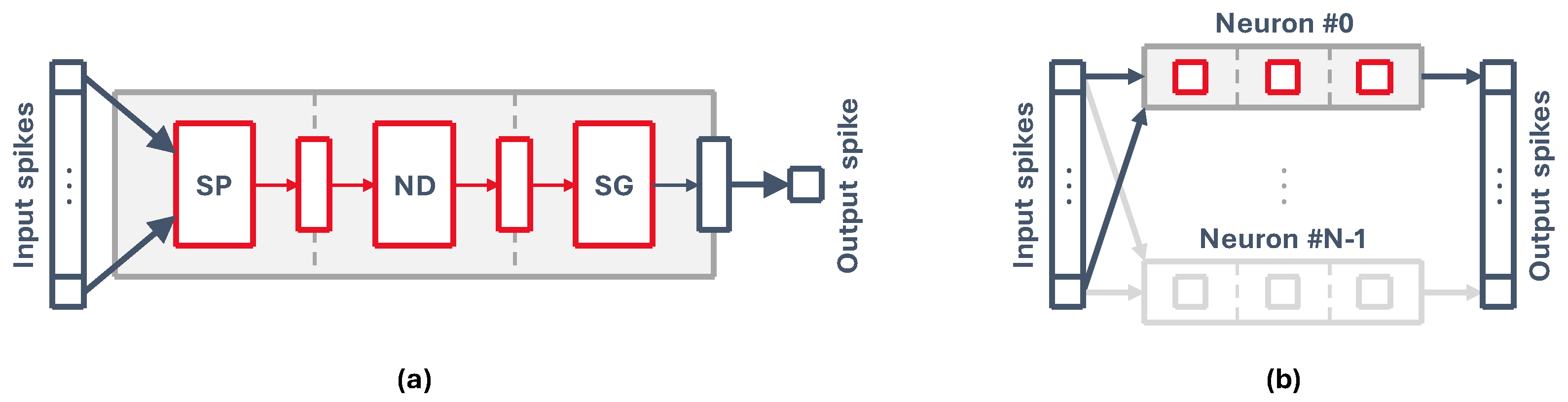
Our implementation is based on the concept of the neuron core as a single unit that can simulate groups of neurons rather than individual neurons. This is a natural consequence of performing a pipelined hardware implementation of a single spiking neuron, like that of
Figure 2a. Grouping together a set of N neurons with M synapses, which are connected to the same presynaptic outputs, allows us to use the same circuit with some additional control hardware to run all neurons sequentially, as represented in
Figure 2b.
By feeding the pipeline with information (i.e., neuron state and weights) from each neuron every cycle, we can process them all to generate a vector of output spikes, essentially simulating a fully connected layer of spiking neurons. A pipelined core takes advantage of some key aspects of high-level SNN description languages, where neurons are usually defined in groups or populations that are easily mapped into neuron cores. These can then be sized accordingly based on the number of neurons and synapses.
Also, all processing inside a neuron model is self-contained, meaning that the information inside each neuron does not depend on other neurons. This, together with the fact that simulation step times (0.1 ms to 10 ms) are usually orders of magnitude larger than typical FPGA clock speeds, makes hardware pipelining an interesting choice. Lastly, since internal states and synaptic weights are accessed sequentially and independently, we can use distributed memory blocks, which are readily available on FPGAs.
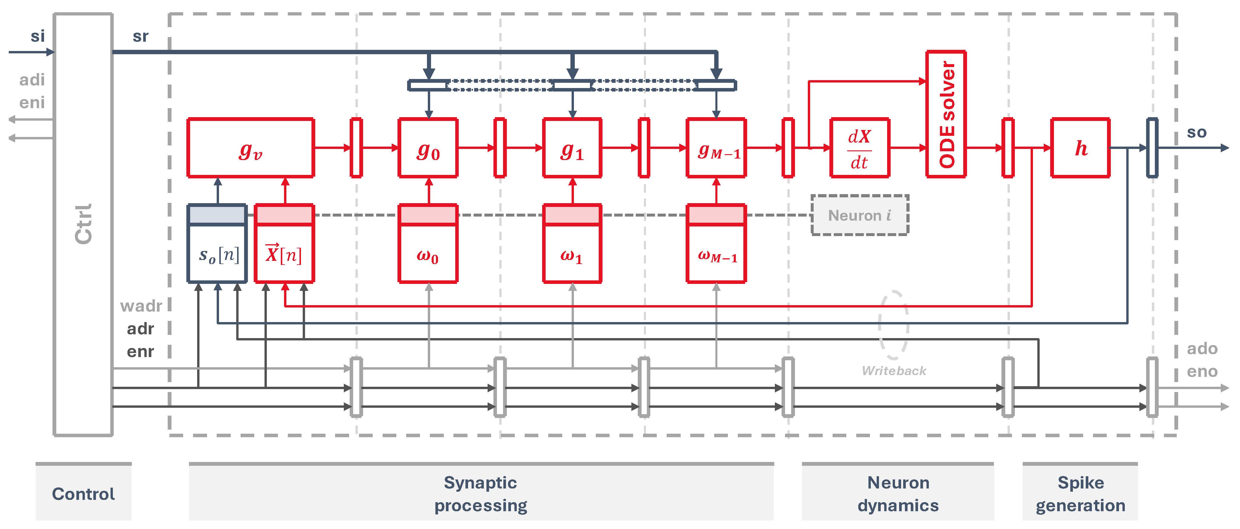
3.1. Architecture
Our circuit, shown in
Figure 3, implements the three main operations: synaptic processing, neuron dynamics, and spike generation. Firstly, the virtual synapse is placed at the beginning of the synaptic processing stage, which fetches from memory the previous neuron state and the output spike information from the last time step, pushing the updated state into the pipeline. After that, each synaptic weight circuit occupies one pipeline stage, pulling data from individual memory elements, where each memory element
i holds
for all
N neurons. This implements Equation (
2) for each one of the neuron synapses.
The next stage calculates the updated state for the next time step using a differential equation solver, as per Equations (
3) and (
4). Lastly, a threshold circuit checks this new state and generates an output spike when the threshold condition is reached, as defined in Equation (
5).
The input spikes are read from an input memory, addressed by the signals adi and eni. To manage the flow of data and feed the pipeline with information from all neurons, a control state machine is laid out at the first stage. It acts as a sort of program counter that generates the input addresses to read the input spikes. It also generates the output neuron addresses, propagating them through every stage to fetch all the weights and state of each neuron. At the end of the pipeline, they are used to update neuron states and output spikes, which are written back into their corresponding memory elements, and to store the outputs into an external spike memory through the signals ado and eno.
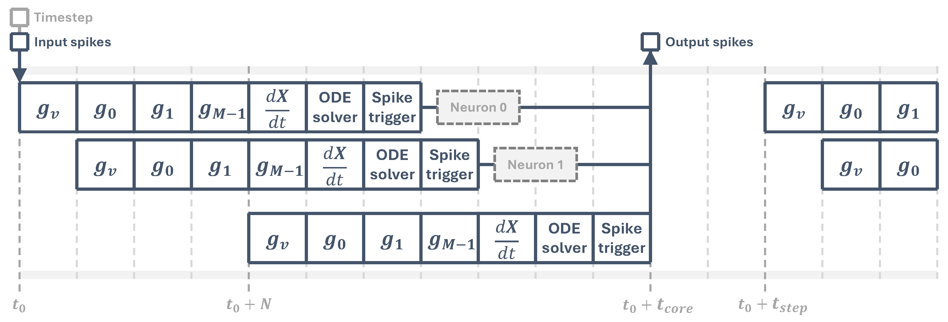
When the time step input signal arrives, which marks the start of one simulation time step, all input spikes are processed sequentially by the synaptic processing stage, then the equation solver updates the neuron states and finally all output spikes are generated, as shown in
Figure 4.
3.2. LIF Core Implementation
Due to its simplicity and low computational cost, the LIF neuron is one of the most used neuron models in spiking neural network simulations [
26]. As illustrated in
Figure 5, we implement a simplified LIF neuron model where the state variable of each neuron is defined as a scalar value,
, holding the membrane voltage, and the core pipeline is implemented as follows:
Synaptic processing: the core implements the synaptic model of Equation (
2), where static weights are used for training and inference. To simplify the implementation, weights can not be updated on the fly and the simulation relies on offline training. The virtual synapse implements the LIF state reset:
taking the previous membrane voltage and resetting it to its rest potential if the neuron has spiked in the previous time step. After that, the following synaptic stages take that updated potential and sequentially process the input spikes:
Neuron dynamics: the state equations are hard-coded into the core definition, although they can be modified before synthesis if the model needs to be changed. The rate of change for this simplified LIF model is a linear function of the difference between the membrane voltage and its resting potential.
where
is the membrane potential after the synaptic processing and
is a parameter that determines how fast the membrane goes back to its resting potential. This coefficient is a power of two to implement the multiplication as a bit shift, but the core can incorporate multipliers if the model needs more generic parameters. The equation solver simply adds this value to the previous state, assimilating the
value into
.
Spike output: the spike output condition function of Equation (
5) is implemented in this case as a simple threshold, which is compared against the state variable
where
is an arbitrary constant threshold potential.
3.3. Latency
Cores need to perform all neuron operations before the next simulation time step arrives. Their latency depends on the number of synapses
M, determining the pipeline length, and the total number of neurons
N. In this LIF implementation, all synaptic and state update operations happen in a single cycle, so we have
where
is the system clock period and
is the core latency, shown in
Figure 4. For the simulation to be able to run, all cores must satisfy
.
Neurons are isolated processing units, which means that they do not need information from other neurons to work. A pipelined implementation like this one is then free of data hazards and, since all synapses have their own stage, control or structural hazards are not a problem either. This allows us to split the core into smaller groups of neurons and parallelize the computations as much as we want. If we divide the total number of neurons by a constant parallelization parameter,
d, and distribute the neurons evenly between cores, we obtain a lower latency value,
and if we do it so that each core only runs one neuron (i.e.,
), we obtain a minimum value for
. This is really useful when mapping high-level descriptions into hardware as it lets us map big groups into smaller cores that are able to keep up with the simulation time step.
3.4. Quantization and Memory
Each neuron holds information about its state , its weights —where i is the synapse number—and their previous output spike . Synapses and neuron dynamics are split up into pipeline stages, so we need distributed memory to fetch all that information separately and continuously. This way, we can overlap the calculations for all neurons along the pipeline.
LIF neuron model implementations can vary, having different numeric representations and specific operations. We have focused on fixed-point 16-bit values to hold the membrane potential and weights, as we consider it large enough to be representative. Also, according to the neuron model rules, all spike events are stored as bits, which is convenient as many commercial FPGAs can implement 1-bit-wide block RAMs.
If a core is sized to run
N neurons, and assuming that all neurons are fully connected and have
M synapses, the needed storage space is
where
m is the total memory usage in bytes. For instance, a core running 64 LIF neurons with 64 possible different synapses needs roughly 4.2 kB of block memory.
4. Convolutional Core
A convolutional layer can be implemented using a fully connected core with N neurons, corresponding to the total number of output pixels, and M synapses per neuron, corresponding to the number of input pixels. It is obvious that this is a very wasteful approach since all neurons have the same weights, and each output neuron only covers a small region of the input feature map, the size of the kernel. This means that only the synaptic weights around that region are meaningful while the remaining weights, and in fact most of them, are zero.
It is worth noting that the concept of spiking convolutional layers emerges from classical Convolutional Neural Networks (CNNs), where biological plausibility is not a concern. Kernels sweep along and across the input feature maps to generate smaller output maps that encode more complex information. However, they have to move around in order to do so; that is, the kernel synapses are not spatially bound to the presynaptic neurons, which does not seem like something that actually happens in biological systems. Because of that, in some ANN-to-SNN converters [
27], convolutional layers are mapped into dense layers that have static synaptic connections, but are way larger than what is required to store kernel information.
Nevertheless, they are computationally useful. In order to design an efficient spiking convolutional core, we can greatly reduce memory usage and area by making a couple modifications to the fully connected neuron core architecture:
Removing all unnecessary zeros: every output neuron only processes information about a small region of the input space. That means that the rest of them are zero and can be ignored. A fully connected layer would have , while a layer with no zero-valued weights would have .
Storing kernel weights only once: all neurons share the same kernel weights, so the number of synaptic weights drops again to .
Emulating kernel stride/movement: by carefully arranging the kernel weights and getting the input information in a certain order, we can take advantage of the input synaptic pipeline to “move” the kernel around. This is performed all while minimizing the amount of intermediate storage needed inside the pipeline.
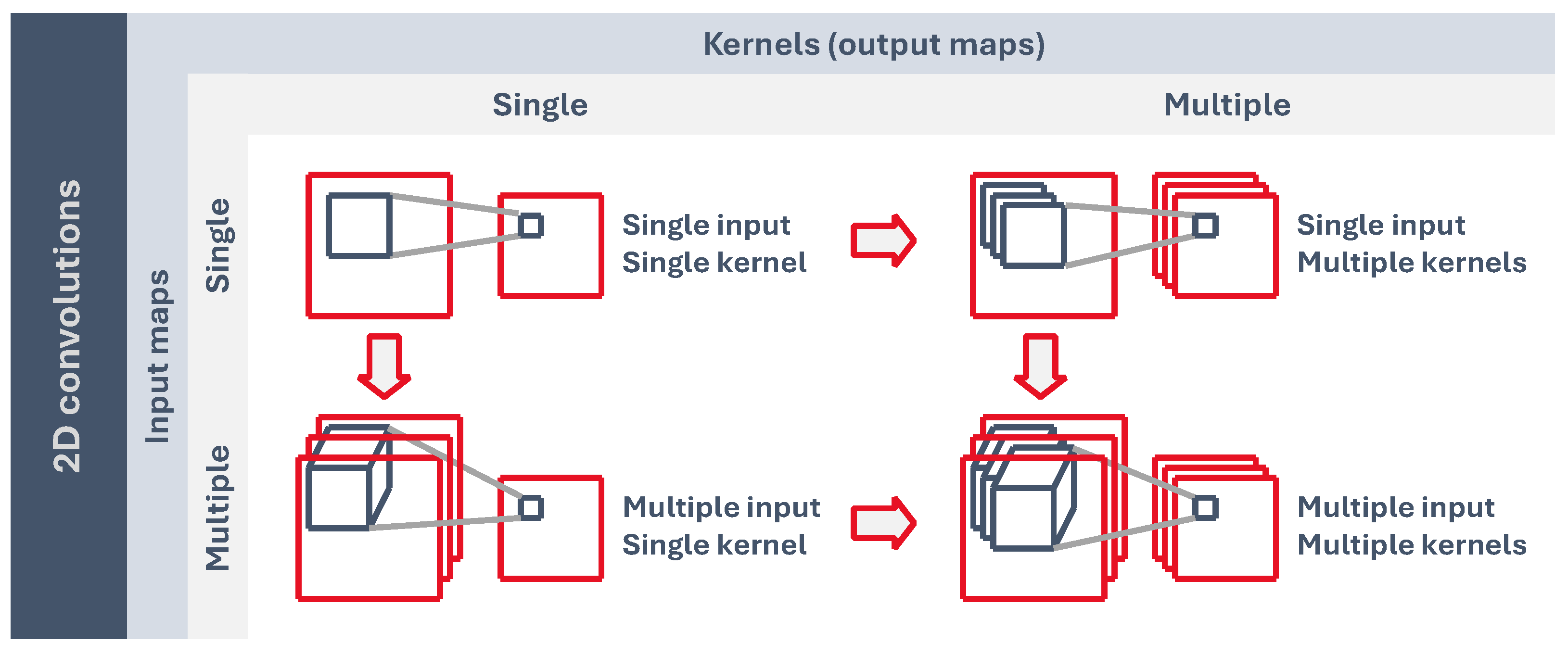
4.1. Two-Dimensional Convolution
As can be seen in
Figure 6, convolutional layers may have a single 2D input feature map, which generates another 2D output map. If we have more than one kernel, the output is a stack of 2D maps. On the other hand, if we have a single kernel, but a stack of 2D input features, then the kernel is 3-dimensional, but we still have a single 2D output feature because the kernel z dimension is equal to the number of inputs, and it only moves along the x and y axis. Lastly, we may have a stack of 2D input features and more than one 3D kernel, which would generate another stack of 2D output maps.
The architecture is understood more clearly if we start from the ground up by building a 2D single-input single-kernel non-pipelined implementation and progressively build our way up to a 2D multi-input multi-kernel pipelined convolutional core.
4.2. Single-Input Single-Kernel 2D Convolution
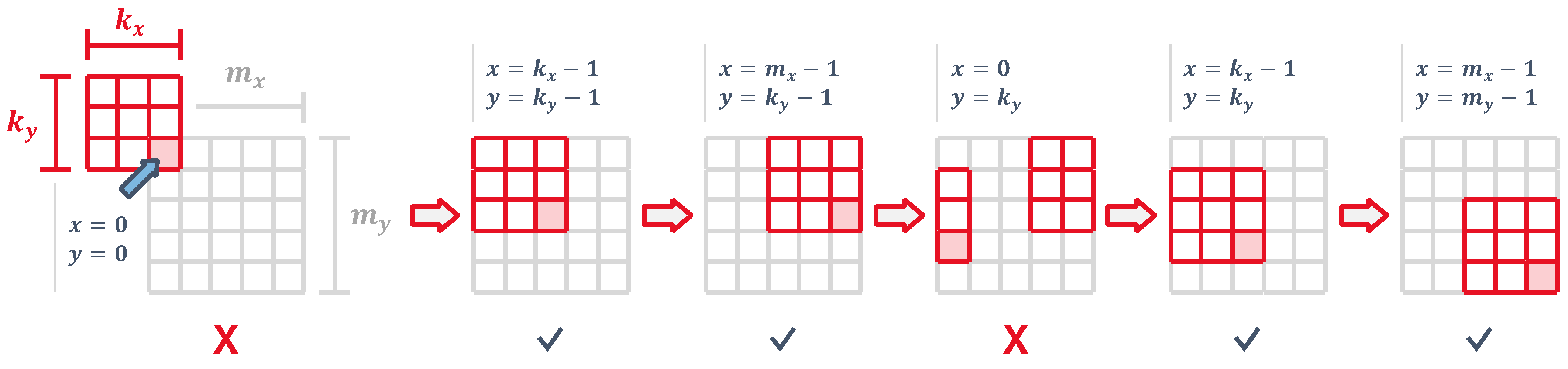
Input spikes are read from the presynaptic output memory and, in the fully connected core, we read and latch the whole input vector into the synaptic pipeline sequentially. This time, the control unit manages a FIFO-like structure called a line buffer where, based on the kernel size, only the necessary information from the input map is available to the pipeline at any time.
Figure 7a shows a representation of the line buffer against an input image, where we can see the pixels that need to be stored at any given time for a single output pixel. When the kernel moves—to the right in this case—we simply shift the new pixel into the line buffer, which is implemented as a long shift register. By carrying out this, we shift the input data in instead of physically moving the kernel around. This way, we can obtain the kernel input image region by taking it from specific locations on the buffer, and we can directly apply the corresponding kernel weights as constant values.
Since the spikes are binary, it is feasible to implement the line buffer as a register rather than with RAM memory. Its length depends on the kernel size
as well as the input map width as
By taking our line buffer and representing it as a straight line, as it is shown in
Figure 7b, we see that it holds
segments of
bits, which correspond to the kernel inputs. As the input data flow in, those segments hold the data for the next stride as if the kernel was moving itself. For a non-pipelined implementation, the output calculation is just a matter of multiplying all the inputs with their corresponding kernel weights and waiting for the next input spike to come in.
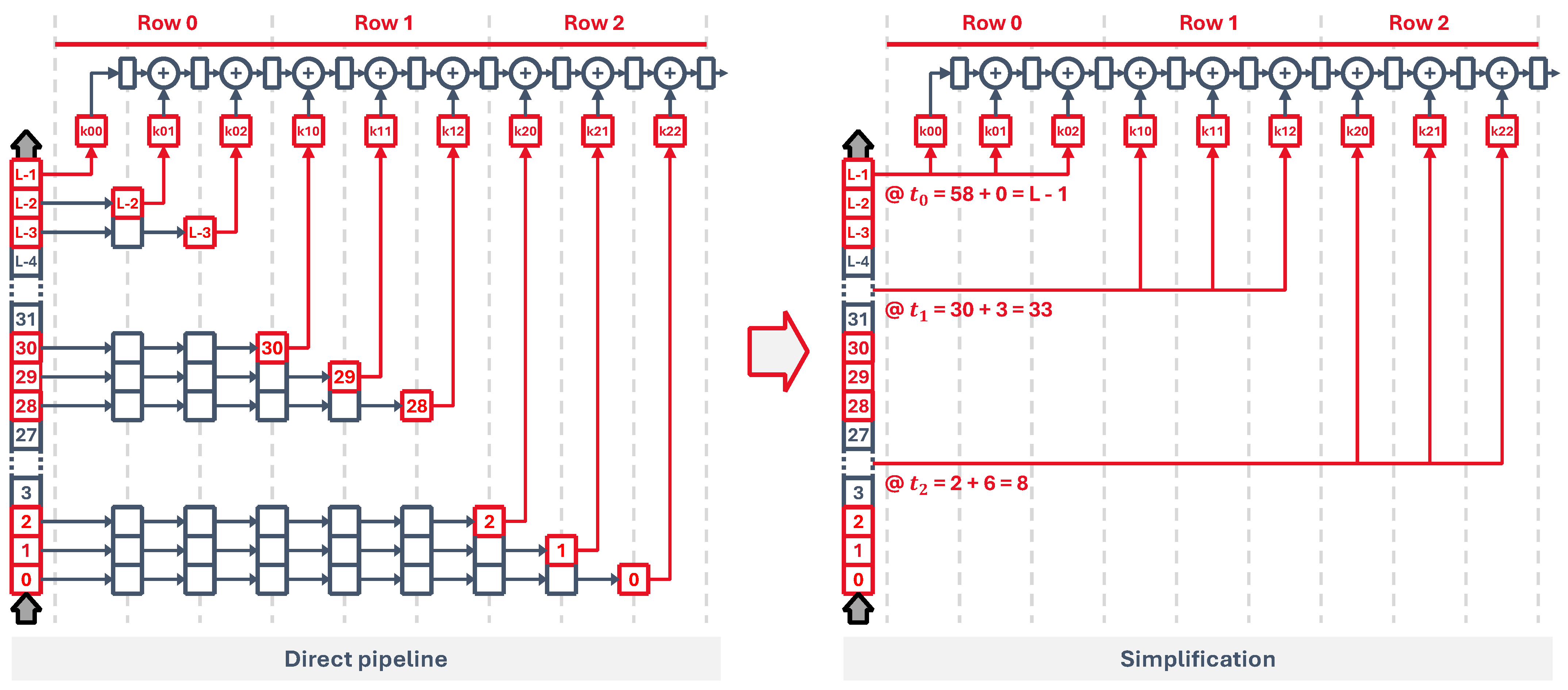
4.2.1. Pipelining
In the next step, we pipeline the implementation into one stage per kernel weight. To that end, we need to copy the line buffer kernel segments into the pipeline, so that each stage obtains all input bits at the right moment, as illustrated in
Figure 8. It can be shown, however, that those copies are not needed at all, since they can be fetched from the line buffer at specific positions up ahead of the shift register as long as the input is read continuously. Every row has its own access point, whose position in the line buffer is given by
where
is the last position in the line buffer for a specific row,
i, and
is the tap point for each row.
The kernel weight order is arbitrary and can be changed, leading to some other configurations with different properties. For instance, if we place the weights in reverse (with respect to the previous implementation), we see that we can also simplify the pipeline, but the line buffer must be bits longer. However, this configuration has a fanout of just one stage per line buffer bit, as opposed to the stages per bit in the forward configuration, which may be of use in high-speed setups.
4.2.2. Control and Padding
Since access to the input feature map is sequential, the core starts by filling in the line buffer with its first row. The control logic uses two counters
x and
y, representing the input map coordinates, and generates an input address to read the flattened image from input memory as
As illustrated in
Figure 9, we are not able to generate an output until the line buffer has enough bits so that the kernel is aligned with the top-left corner, which causes the pipeline to generate dummy values for the first cycles. During this time, the control logic generates a rejection signal and the outputs are discarded. In a similar way, when the kernel reaches the right edge of the input feature map, we need to wait
cycles for the kernel to wrap around and get back to the left side. During this time, the outputs are also ignored. Both conditions can be combined into
The output map has a size of
by
. Output addresses are generated, which can be expressed as a function of the current
input pixel as
We focus on generating a convolution with no padding since it is the most straightforward to implement. However, the line buffer could be filled with zeros at the correct times to perform a convolution with input padding.
4.3. Multiple-Input Single-Kernel 2D Convolution
When jumping onto convolutions of multiple 2D input maps, the kernel turns into a 3D object that runs along the
x and
y axes. Generally, to move the kernel along a specific axis,
j, and compute its output, one needs to read a new set,
S, of input pixels. This set contains the pixels in the plane next to the current position in the direction of the axis. The number of new pixels is
where
i represents all axes except for the one the kernel is moving along, and
is the kernel size along axis
i. Since we chose to move through the
x axis first, we would need to obtain
input pixels every time we want to compute a new output pixel. However, thanks to the line buffer, we already have some of the previous values ready to go, so the actual number of pixels to be read every time drops to
. We also keep the previous strategy of discarding the outputs while the kernel is rolling over the edges in the
x dimension.
The control logic assumes that the input maps are stored sequentially, so their pixel values are not interlaced. The input address generation then changes to
The fact that we have to wait for all pixels in the z dimension to generate a single output is not a problem as long as the control logic keeps track of the kernel alignment. While the input pixels are loaded in, the circuit rejects all generated output values until the line buffer contents are properly aligned with the kernel weights, that is, every
read. The alignment condition turns into
Now, instead of reading in single pixels, we read all input map values for every
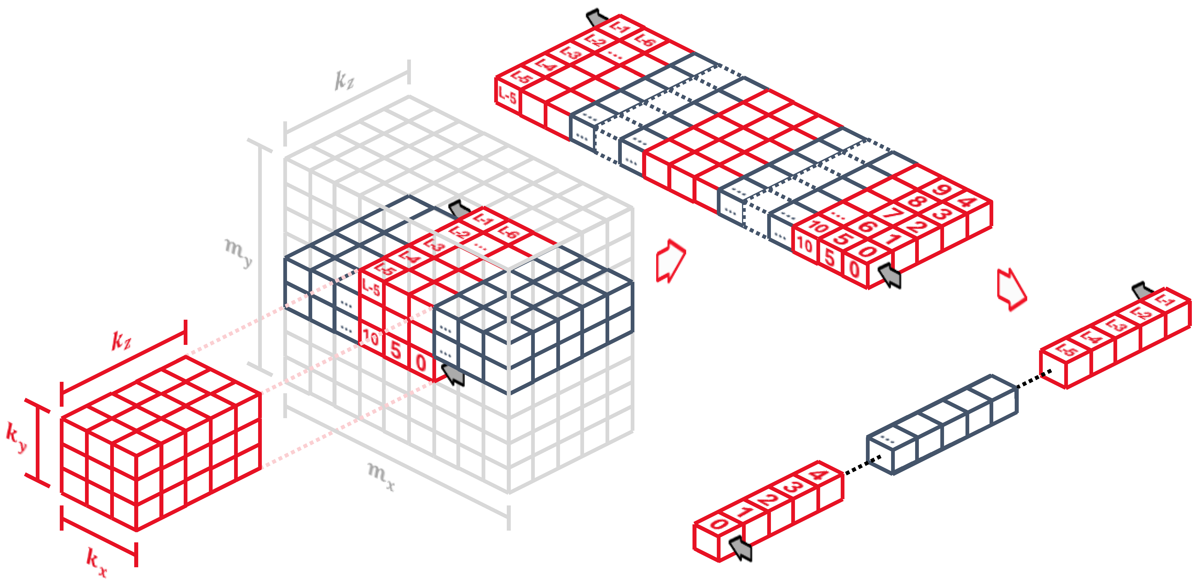
pixel and store them sequentially into the line buffer, as shown in
Figure 10, so for every pixel, we store a vector of
values. It is the most convenient way of going through all input maps: the kernel
z dimension is equal to the number of maps, so as soon as we compute an output pixel, we can completely discard the last values in the line buffer without having to read them again.
Since the line buffer holds
values for every pixel, the buffer length is now
The row and tap positions also change slightly, but they still keep the convenient property of being static locations in the line buffer regardless of the kernel
z dimension, as long as the kernel values are properly connected along the synaptic pipeline. They become
4.4. Multiple-Input Multiple-Kernel 2D Convolution
To extend this architecture to support multiple kernels so that the output is a stack of 2D feature maps, we look back to the fully-connected synaptic architecture. While the previous convolutions had constant kernel weights, in this case, we add a small array of weights holding all kernels along the pipeline stages, as shown in
Figure 11.
By combining the two previous strategies, we can build the most general case where multiple input maps are processed with multiple 2D kernels to generate a stack of 2D output feature maps. The controller reads all input maps once per kernel, sequentially computing the corresponding output maps, whose dimensions are
by
. The output addresses to store the output maps in memory are generated based on the
input pixel coordinates and the kernel index
f as
5. Core-Based SNN Implementation
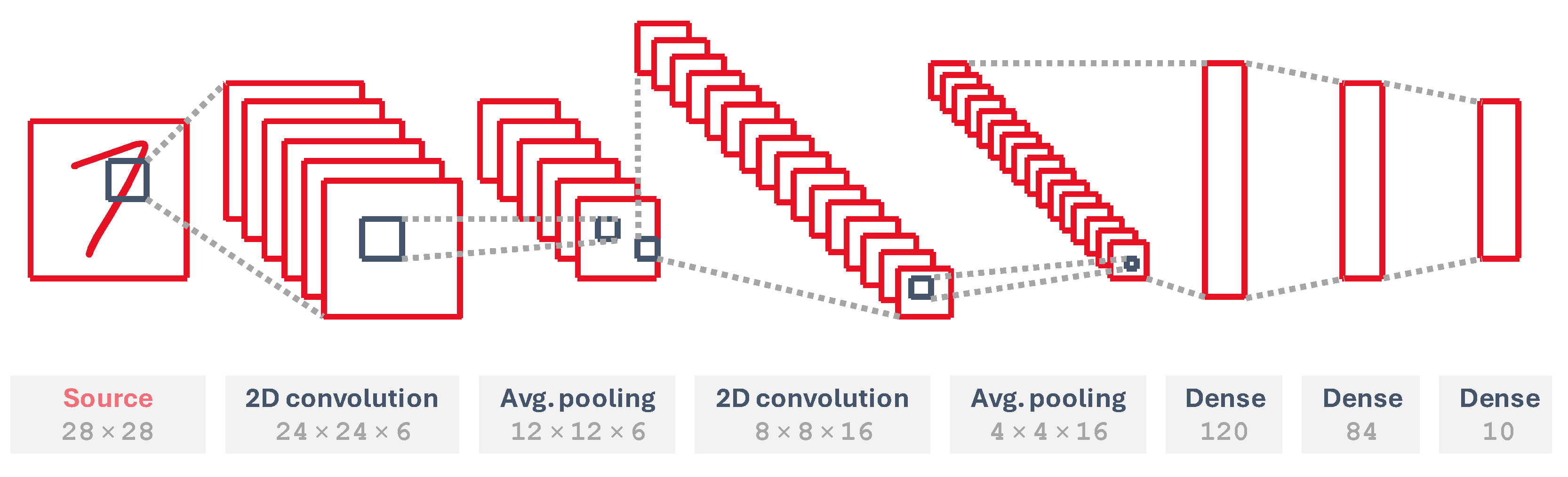
To showcase the performance of the developed modules, we implement an SNN version of a LeNet-5 network [
28], shown in
Figure 12, which is a neural network architecture for handwritten and machine-printed character recognition, trained on the handwritten digit MNIST dataset [
29]. It consists of two convolutional layers; two average pooling layers, which subsample the input features and average their pixels out to generate smaller feature maps; and three fully connected layers. It is a convenient way to demonstrate an application that fits in a low-power device on the edge. This network has been trained as a classical ANN in Keras and converted into an SNN using the SNN toolbox framework [
27].
The input layer converts input images into Poisson rate-coded spikes. We map all other layers into several cores, using both the fully connected and 2D convolutional versions. To implement the pooling layers, which have a 2 × 2 pooling mask, we use a single-input single-kernel 2D convolutional layer with all weights equal to
and stride
, applied as many times as input feature maps in the previous convolutional layer. The rest of them have several sets of trainable weights, whose number is shown in
Table 1.
All layers start their processing when the global time step signal arrives, reading their input spikes and storing the generated output spikes back into a series of dual-port memories that chain all layers together, as illustrated in
Figure 13. The spike memories are instantiated by the synthesizer, which is free to choose any device primitive. However, due to their relative small size compared to the synaptic weights and the fact that they hold binary values, they are implemented as distributed RAM that can be read and written by all layers at the same time.
For example, the first 2D convolution reads the 784 bits from the input memory through the si, adi, and eni interface. After processing, it writes the 3456 output bits (binary spikes) to the next memory block through so, ado, and eno. The total number of spike memory bits for the whole network is equal to the number of neurons in the network, which in this case is .
Regarding weight and state memory usage, the total number of bits is given by
where
N is the total number of neurons,
W is the total number of weights in the network, and
m is the memory requirement in bits. For this network,
800,192 bit = 781.4 kB.
The input layer module is loaded with an MNIST image to generate the network input spikes, which are processed by the following layers. The final output spikes are available through the read interface of the last memory block after all the processing is complete.
6. Results
The cores and network have been developed in VHDL using Xilinx Vivado 2022.1 and GHDL, and have been synthesized and tested on a Xilinx Artix-7 XC7A100T FPGA. We opted for a relatively compact device as our focus is on low-power and low-area applications.
Table 2 shows the primitive utilization of the whole network with 16-bit-wide weights. To have as reusable a design as possible, all Hardware Description Language (HDL) code has been written using no vendor- or device-specific instances. All memories have been coded to be synchronous but, besides that, primitive inference is then left to the synthesizer, which has control over what type of memory it instantiates for weight, neuron state, and spike storage. It can be seen that different layers use different elements: the convolutional and pooling layers rely on a mix of distributed memory, LUTs, and block RAM, while the two biggest fully connected ones use up the available block RAM tiles. We have seen that this distribution is consistent even in bigger FPGAs with more available memory, so block RAM utilization is not limited by device size but rather by the synthesis optimization process.
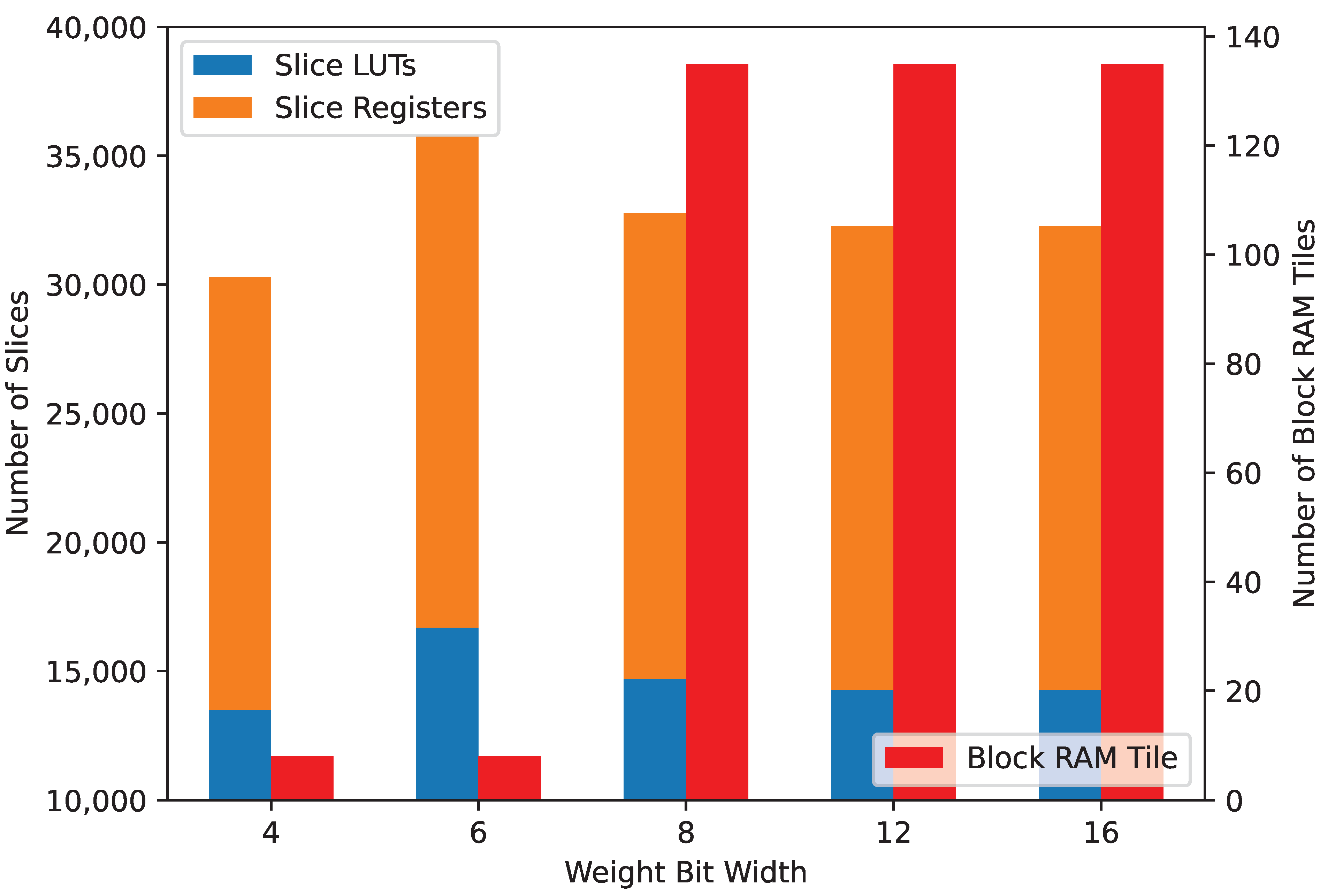
We have tested the network architecture for different weight quantization bit widths, from 4 to 16 bits. While the cores remain the same with no remarkable difference in resource usage, the weight storage distribution changes and in
Figure 14, it can be seen that the synthesizer switches to block RAM for weight storing as bit widths go past 8 bits. None of the implementations use any of the available digital signal processing (DSP) slices in the FPGA.
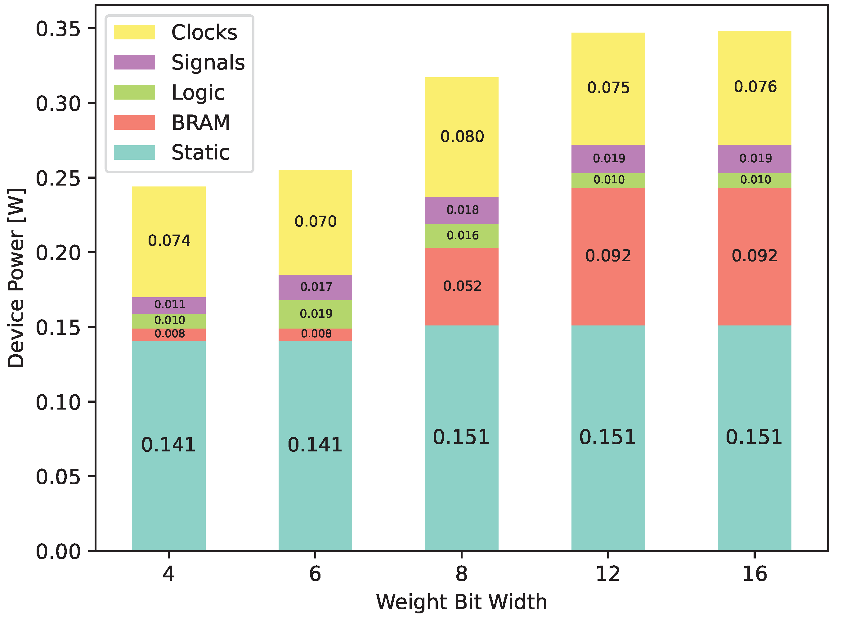
Using switching activity data from post-implementation simulations to obtain a more realistic power figure, we performed a power analysis to obtain the estimated energy consumption, which can be found in
Table 3. Shown in
Figure 15, we can see that this switch to RAM drives energy consumption up from 0.244
for 4 bits to 0.348
for 16 bits.
6.1. Latency and Minimum Time Step
Since all layers process data simultaneously, the minimum time step the network simulation can achieve is dependent on the maximum latency among all of them. In this case, the longest processing time is reached by the second 2D convolutional layer, mostly because of the number of kernels and kernel size. At 13,978 cycles, it translates to μs for a system clock frequency of 132 MHz.
Both fully connected and convolutional cores can take advanatage of the data independence between neurons to be parallelized. This could be exploited to split each layer into several cores, each of which would process a subset of the neurons in that layer. This way, we could shorten the maximum latency values, trading in area for speed to achieve shorter simulation time steps, or to fit larger layers in a lower-speed device.
6.2. Benchmarking
Table 4 shows a comparison between the previously mentioned state-of-the-art FPGA SNN accelerators. We considered a representative set of relevant implementations based on LIF neurons. It can be seen that, while block RAM and distributed memory usage is similar, our cores manage to reach the lowest resource utilization per neuron among the considered architectures, at 2.45 and 3.10 LUTs and Flip-Flops (FFs) per neuron, respectively. Our minimum step time of about 140 μs is small enough to fit the lowest times commonly employed in these simulations, which are usually in the hundreds of microseconds, and the whole network runs at only 348 mW or 59.86 μW/neuron when using the largest weight and state bit widths, making it the least power-hungry implementation.
Making comparisons between FPGA-based SNN implementations is not straightforward. Almost every one of them runs similar realizations of the Leaky-Integrate-and-Fire neuron model, but they do so on many different FPGA platforms with largely varying available resources and speed capabilities. To make things worse, they implement different network architectures with different quantization levels and memory organization, which significantly impact the implementation results. For instance, a network with more convolutional layers will see a decrease in LUTs and FFs per neuron since many neurons are simulated using a single set of kernel weights.
More importantly, state-of-the-art design analyses usually put their emphasis on network accuracy or fitness, which are application-derived metrics rather than architectural ones. Since our focus is on hardware optimization, we have provided as much characterization data as possible to compensate for the lack of algorithmic-level comparative figures. Our goal is to construct a circuit architecture that can accommodate any high-level description, independent of the neural model and network topology—which will determine the accuracy-related metrics—while being optimized for efficient and light-weight close-to-the-edge systems. To achieve ultra-low area and power consumption, as well as low simulation step times, we leverage the strengths of clock-driven architectures and employ two key strategies: extensive and extreme hardware pipelining, specially convenient for FPGA platforms and distributed memory to increase weight access bandwidth, and a fixed connectivity scheme that relies on efficient spike memory banks.
7. Conclusions
This work introduces a new architecture for the acceleration of SNNs, using clock-driven neuron processing cores on FPGAs. It is able to reach fast simulation step times of 105.9 μs and, using 16-bit-wide neuron states and weights, it has the lowest device resource utilization among all compared works, at 5.55 slices per neuron, respectively, as well as the lowest power figure at 59.86 μW per neuron.
It is based on the concept of the neuron core as a unit capable of simulating groups of spiking neurons, which
Takes advantage of pipelining and neuron data independence to accelerate simulations and reduce hardware usage, using around 33% less slices per neuron than the best current implementation.
Achieves very-low-power operation, nearly four times less power per neuron compared to the most efficient state-of-the-art accelerator.
Manages to keep simulation step times low, which contributes to making more accurate simulations and leaves room for bigger networks.
Makes it easy to map high-level descriptions of SNNs into hardware.
We define control subsystems for fully connected and 2D convolutional layers, spanning from single-map single-kernel instances to fully fledged multimap 2D convolutions with multiple kernels.
The presented cores are flexible circuits designed to run arbitrary models. They are meant to be used as building blocks in automatic mapping from network description languages to FPGA-based SNN accelerators, enabling designers to easily generate fast and efficient hardware from any supported neuron model. Our simplified LIF neuron is a good starting point for implementing new supported models, performing accuracy tests, or developing different connectivity schemes for many types of neuron layers.
Using the SNN toolbox for ANN-to-SNN conversion, we developed an implementation of the LeNet-5 architecture trained on the MNIST handwritten digit dataset to showcase our convolutional and fully connected cores. We have not gone further into training or inference and instead we have focused on optimizing circuit area, timing, and power, trying to decouple hardware design parameters from figures of merit related to neural networks such as accuracy.
To this end, a support software framework relying on our core architecture would allow us to make such comparisons much more easily. Automatically mapping high-level network descriptions into HDL code and passing dataset information to the FPGA device would enable quick and easy testing with different parameters, models, and quantization levels. This would allow us to give performance and accuracy values on real hardware tailored for close-to-the-edge applications on low-resource devices.
Author Contributions
Conceptualization, S.L.-A. and P.I.; methodology, S.L.-A.; software, S.L.-A.; validation, S.L.-A. and P.I.; formal analysis, S.L.-A.; investigation, S.L.-A.; resources, S.L.-A. and P.I.; data curation, S.L.-A.; writing—original draft preparation, S.L.-A. and P.I.; writing—review and editing, S.L.-A. and P.I.; visualization, S.L.-A.; supervision, P.I.; project administration, P.I.; funding acquisition, S.L.-A. and P.I. All authors have read and agreed to the published version of the manuscript.
Funding
This research was funded by the MCIN/AEI/10.13039/501100011033 Spanish Ministry of Science and Innovation within projects PID2022-141391OB-C21 and PDC2022-133657-I00, and grant PGC2018-097339-B-I00.
Data Availability Statement
The data are available on request to the corresponding authors.
Conflicts of Interest
The authors declare no conflicts of interest. The funders had no role in the design of the study; in the collection, analyses, or interpretation of data; in the writing of the manuscript; or in the decision to publish the results.
References
- Maass, W. Networks of spiking neurons: The third generation of neural network models. Neural Netw. 1997, 10, 1659–1671. [Google Scholar] [CrossRef]
- Kasabov, N.K. Time-Space, Spiking Neural Networks and Brain-Inspired Artificial Intelligence; Springer: Berlin/Heidelberg, Germany, 2019. [Google Scholar]
- Yamazaki, K.; Vo-Ho, V.K.; Bulsara, D.; Le, N. Spiking Neural Networks and Their Applications: A Review. Brain Sci. 2022, 12, 863. [Google Scholar] [CrossRef] [PubMed]
- Frenkel, C.; Bol, D.; Indiveri, G. Bottom-Up and Top-Down Neural Processing Systems Design: Neuromorphic Intelligence as the Convergence of Natural and Artificial Intelligence. arXiv 2021, arXiv:2106.01288. [Google Scholar]
- Bogdan, P.A.; Marcinnò, B.; Casellato, C.; Casali, S.; Rowley, A.G.; Hopkins, M.; Leporati, F.; D’Angelo, E.; Rhodes, O. Towards a Bio-Inspired Real-Time Neuromorphic Cerebellum. Front. Cell. Neurosci. 2021, 15, 622870. [Google Scholar] [CrossRef]
- Pei, J.; Deng, L.; Song, S.; Zhao, M.; Zhang, Y.; Wu, S.; Wang, G.; Zou, Z.; Wu, Z.; He, W.; et al. Towards artificial general intelligence with hybrid Tianjic chip architecture. Nature 2019, 572, 106–111. [Google Scholar] [CrossRef] [PubMed]
- Indiveri, G. Computation in Neuromorphic Analog VLSI Systems. In Perspectives in Neural Computing; Springer: London, UK, 2002; pp. 3–20. [Google Scholar]
- Davidson, S.; Furber, S.B. Comparison of Artificial and Spiking Neural Networks on Digital Hardware. Front. Neurosci. 2021, 15, 651141. [Google Scholar] [CrossRef]
- Basu, A.; Deng, L.; Frenkel, C.; Zhang, X. Spiking Neural Network Integrated Circuits: A Review of Trends and Future Directions. In Proceedings of the 2022 IEEE Custom Integrated Circuits Conference (CICC), Newport Beach, CA, USA, 24–27 April 2022; pp. 1–8. [Google Scholar]
- Golosio, B.; Tiddia, G.; Luca, C.D.; Pastorelli, E.; Simula, F.; Paolucci, P.S. Fast Simulations of Highly-Connected Spiking Cortical Models Using GPUs. Front. Comput. Neurosci. 2021, 15, 627620. [Google Scholar] [CrossRef]
- Furber, S.B.; Lester, D.R.; Plana, L.A.; Garside, J.D.; Painkras, E.; Temple, S.; Brown, A.D. Overview of the SpiNNaker System Architecture. IEEE Trans. Comput. 2013, 62, 2454–2467. [Google Scholar] [CrossRef]
- Akopyan, F.; Sawada, J.; Cassidy, A.; Alvarez-Icaza, R.; Arthur, J.; Merolla, P.; Imam, N.; Nakamura, Y.; Datta, P.; Nam, G.J.; et al. TrueNorth: Design and Tool Flow of a 65 mW 1 Million Neuron Programmable Neurosynaptic Chip. IEEE Trans. Comput.-Aided Des. Integr. Circuits Syst. 2015, 34, 1537–1557. [Google Scholar] [CrossRef]
- Davies, M.; Srinivasa, N.; Lin, T.H.; Chinya, G.; Cao, Y.; Choday, S.H.; Dimou, G.; Joshi, P.; Imam, N.; Jain, S.; et al. Loihi: A Neuromorphic Manycore Processor with On-Chip Learning. IEEE Micro 2018, 38, 82–99. [Google Scholar] [CrossRef]
- Deng, L.; Wang, G.; Li, G.; Li, S.; Liang, L.; Zhu, M.; Wu, Y.; Yang, Z.; Zou, Z.; Pei, J.; et al. Tianjic: A Unified and Scalable Chip Bridging Spike-Based and Continuous Neural Computation. IEEE J. Solid-State Circuits 2020, 55, 2228–2246. [Google Scholar] [CrossRef]
- Pham, Q.T.; Nguyen, T.Q.; Hoang, P.C.; Dang, Q.H.; Nguyen, D.M.; Nguyen, H.H. A review of SNN implementation on FPGA. In Proceedings of the 2021 International Conference on Multimedia Analysis and Pattern Recognition (MAPR), Hanoi, Vietnam, 15–16 October 2021. [Google Scholar]
- Davison, A.; Brüderle, D.; Eppler, J.; Kremkow, J.; Muller, E.; Pecevski, D.; Perrinet, L.; Yger, P. PyNN: A common interface for neuronal network simulators. Front. Neuroinform. 2009, 2, 11. [Google Scholar] [CrossRef] [PubMed]
- Brette, R.; Rudolph, M.; Carnevale, T.; Hines, M.; Beeman, D.; Bower, J.M.; Diesmann, M.; Morrison, A.; Goodman, P.H.; Harris, F.C., Jr.; et al. Simulation of networks of spiking neurons: A review of tools and strategies. J. Comput. Neurosci. 2007, 23, 349–398. [Google Scholar] [CrossRef] [PubMed]
- Neil, D.; Liu, S.C. Minitaur, an Event-Driven FPGA-Based Spiking Network Accelerator. IEEE Trans. Very Large Scale Integr. (VLSI) Syst. 2014, 22, 2621–2628. [Google Scholar] [CrossRef]
- Mo, L.; Tao, Z. EvtSNN: Event-driven SNN simulator optimized by population and pre-filtering. Front. Neurosci. 2022, 16, 944262. [Google Scholar] [CrossRef]
- Ma, D.; Shen, J.; Gu, Z.; Zhang, M.; Zhu, X.; Xu, X.; Xu, Q.; Shen, Y.; Pan, G. Darwin: A neuromorphic hardware co-processor based on spiking neural networks. J. Syst. Archit. 2017, 77, 43–51. [Google Scholar] [CrossRef]
- Gupta, S.; Vyas, A.; Trivedi, G. FPGA Implementation of Simplified Spiking Neural Network. In Proceedings of the 2020 27th IEEE International Conference on Electronics, Circuits and Systems (ICECS), Glasgow, Scotland, 23–25 November 2020. [Google Scholar]
- Wang, Q.; Li, Y.; Shao, B.; Dey, S.; Li, P. Energy efficient parallel neuromorphic architectures with approximate arithmetic on FPGA. Neurocomputing 2017, 221, 146–158. [Google Scholar] [CrossRef]
- Liu, Y.; Chen, Y.; Ye, W.; Gui, Y. FPGA-NHAP: A General FPGA-Based Neuromorphic Hardware Acceleration Platform with High Speed and Low Power. IEEE Trans. Circuits Syst. I Regul. Pap. 2022, 69, 2553–2566. [Google Scholar] [CrossRef]
- Gerlinghoff, D.; Wang, Z.; Gu, X.; Goh, R.S.M.; Luo, T. E3NE: An End-to-End Framework for Accelerating Spiking Neural Networks With Emerging Neural Encoding on FPGAs. IEEE Trans. Parallel Distrib. Syst. 2022, 33, 3207–3219. [Google Scholar] [CrossRef]
- Carpegna, A.; Savino, A.; Carlo, S.D. Spiker: An FPGA-optimized Hardware accelerator for Spiking Neural Networks. In Proceedings of the 2022 IEEE Computer Society Annual Symposium on VLSI (ISVLSI), Paphos, Cyprus, 4–6 July 2022. [Google Scholar]
- Taherkhani, A.; Belatreche, A.; Li, Y.; Cosma, G.; Maguire, L.P.; McGinnity, T. A review of learning in biologically plausible spiking neural networks. Neural Netw. 2020, 122, 253–272. [Google Scholar] [CrossRef]
- Rueckauer, B.; Lungu, I.A.; Hu, Y.; Pfeiffer, M.; Liu, S.C. Conversion of Continuous-Valued Deep Networks to Efficient Event-Driven Networks for Image Classification. Front. Neurosci. 2017, 11, 682. [Google Scholar] [CrossRef] [PubMed]
- Lecun, Y.; Bottou, L.; Bengio, Y.; Haffner, P. Gradient-based learning applied to document recognition. Proc. IEEE 1998, 86, 2278–2324. [Google Scholar] [CrossRef]
- Deng, L. The MNIST database of handwritten digit images for machine learning research. IEEE Signal Process. Mag. 2012, 29, 141–142. [Google Scholar] [CrossRef]
Figure 1.
Schematic view of the three neuron model rules.
Figure 1.
Schematic view of the three neuron model rules.
Figure 2.
(a) Simplified view of a pipelined implementation of a generic neuron model. A single neuron accepts an array of input spikes connected one to one to the neuron synapses and generates a single output spike. SP = Synaptic Processing, ND = Neuron Dynamics, SG = Spike Generation. (b) Representation of the core neuron group: a core can process N neurons that have the same M input spikes, generating N outputs.
Figure 3.
Hardware schematic of the pipelined neuron cores, showing the synaptic processing, dynamics, and spike generation stages.
Figure 3.
Hardware schematic of the pipelined neuron cores, showing the synaptic processing, dynamics, and spike generation stages.
Figure 4.
Core processing timeline. Following the first simulation time step at , the core feeds the pipeline with neuron data and processes the input spikes, generating an output spike vector at , where is the core latency. In this diagram, it is assumed that all operations take one clock cycle.
Figure 4.
Core processing timeline. Following the first simulation time step at , the core feeds the pipeline with neuron data and processes the input spikes, generating an output spike vector at , where is the core latency. In this diagram, it is assumed that all operations take one clock cycle.
Figure 5.
Simplified Leaky-Integrate-and-Fire implementation of a fully connected core, with the virtual synapse , synaptic stages , neuron dynamics , and spike generation stage h.
Figure 5.
Simplified Leaky-Integrate-and-Fire implementation of a fully connected core, with the virtual synapse , synaptic stages , neuron dynamics , and spike generation stage h.
Figure 6.
Two-dimensional convolutional layer configurations based on the number of inputs and kernels (outputs).
Figure 6.
Two-dimensional convolutional layer configurations based on the number of inputs and kernels (outputs).
Figure 7.
(a) Line buffer against a 28 × 28 2D image. (b) A 5 × 5 kernel correspondence to the line buffer pixels.
Figure 7.
(a) Line buffer against a 28 × 28 2D image. (b) A 5 × 5 kernel correspondence to the line buffer pixels.
Figure 8.
Single-input single-kernel 2D convolution implementation, 3 × 3 kernel on 28 × 28 input image, pre- and post-simplification.
Figure 8.
Single-input single-kernel 2D convolution implementation, 3 × 3 kernel on 28 × 28 input image, pre- and post-simplification.
Figure 9.
Kernel alignment of the single-input single-kernel 2D convolution. A control signal is generated when the kernel is within the image boundaries and the outputs are valid.
Figure 9.
Kernel alignment of the single-input single-kernel 2D convolution. A control signal is generated when the kernel is within the image boundaries and the outputs are valid.
Figure 10.
Three-dimensional line buffer against a stack of five 2D input maps for a 3 × 3 × 5 kernel. The 3D buffer unfolds to be implemented as a linear shift register.
Figure 10.
Three-dimensional line buffer against a stack of five 2D input maps for a 3 × 3 × 5 kernel. The 3D buffer unfolds to be implemented as a linear shift register.
Figure 11.
Single-input multiple-kernel 2D convolution implementation with 3 × 3 kernels. The same architecture is used in multiple-input multiple-kernel implementations.
Figure 11.
Single-input multiple-kernel 2D convolution implementation with 3 × 3 kernels. The same architecture is used in multiple-input multiple-kernel implementations.
Figure 12.
LeNet-5 architecture for a 28 × 28 MNIST input image and 10 output classes.
Figure 12.
LeNet-5 architecture for a 28 × 28 MNIST input image and 10 output classes.
Figure 13.
SNN network architecture: input, convolutional, pooling, and fully connected neuron cores attached to the spike memory.
Figure 13.
SNN network architecture: input, convolutional, pooling, and fully connected neuron cores attached to the spike memory.
Figure 14.
Slice LUT, register, and block RAM utilization.
Figure 14.
Slice LUT, register, and block RAM utilization.
Figure 15.
Power estimation data @ 100 MHz and 25 °C.
Figure 15.
Power estimation data @ 100 MHz and 25 °C.
Table 1.
Number of neurons, synapses, and weights per layer.
Table 1.
Number of neurons, synapses, and weights per layer.
| | 2D Conv. | Pooling | 2D Conv. | Pooling | Dense | Dense | Dense | Total |
|---|
| | (24 × 24 × 6)
| (12 × 12 × 6)
| (8 × 8 × 16)
| (4 × 4 × 16)
| (120)
| (84)
| (10)
|
|---|
| Neurons | 3456 | 864 | 1024 | 256 | 120 | 84 | 10 | 5814 |
| Synapses | 86,400 | 3456 | 153,600 | 1024 | 30,720 | 10,080 | 840 | 286,120 |
| Weights | 150 | 4 | 2400 | 4 | 30,720 | 10,080 | 840 | 44,198 |
Table 2.
FPGA resource utilization for a LeNet-5 architecture with 16-bit-wide weights (Artix-7 XC7A100TCSG324-1).
Table 2.
FPGA resource utilization for a LeNet-5 architecture with 16-bit-wide weights (Artix-7 XC7A100TCSG324-1).
| | Slice | Slice | Slices | LUT as | LUT as | Block |
|---|
| | LUTs
| Registers
| Logic
| Memory
| RAM 1 |
|---|
| Input | 21 | 38 | 13 | 21 | 0 | 0 |
| 2D conv. (24 × 24 × 6) | 564 | 709 | 184 | 547 | 17 | 2.5 |
| Pooling (12 × 12 × 6) | 98 | 129 | 51 | 87 | 11 | 1 |
| 2D conv. (8 × 8 × 16) | 3420 | 3984 | 1044 | 2973 | 447 | 0 |
| Pooling (4 × 4 × 16) | 81 | 117 | 42 | 67 | 14 | 0.5 |
| Dense (120) | 5890 | 7184 | 1986 | 5878 | 12 | 68.5 |
| Dense (84) | 2128 | 3062 | 789 | 2118 | 10 | 60.5 |
| Dense (10) | 2051 | 2783 | 654 | 2033 | 18 | 0 |
| Spike memory | 15 | 4 | 6 | 1 | 14 | 2 |
| Total | 14,266 | 18,010 | 4744 | 13,723 | 543 | 135 |
| Total (%) | 22.5% | 14.2% | 29.9% | 21.7% | 2.9% | 100% |
| Available | 63,400 | 126,800 | 15,850 | 63,400 | 19,000 | 135 |
Table 3.
Power data and max. frequency values for weight bit widths from 4 to 16 bits.
Table 3.
Power data and max. frequency values for weight bit widths from 4 to 16 bits.
| Bits | Logic | Signals | Clocks | BRAM | Dynamic | Static | Total 1 | Max. Freq. |
|---|
| [W]
| [MHz]
|
|---|
| 4 | 0.010 | 0.011 | 0.074 | 0.008 | 0.103 | 0.141 | 0.244 | 141.80 |
| 6 | 0.019 | 0.017 | 0.070 | 0.008 | 0.114 | 0.141 | 0.254 | 148.96 |
| 8 | 0.016 | 0.018 | 0.080 | 0.052 | 0.166 | 0.151 | 0.317 | 132.53 |
| 12 | 0.010 | 0.019 | 0.075 | 0.092 | 0.196 | 0.151 | 0.347 | 134.31 |
| 16 | 0.010 | 0.019 | 0.076 | 0.092 | 0.197 | 0.151 | 0.348 | 139.31 |
Table 4.
Comparison of relevant state-of-the-art FPGA SNN hardware accelerators.
Table 4.
Comparison of relevant state-of-the-art FPGA SNN hardware accelerators.
| | Minitaur [18] | Wang et al. [22] | Darwin [20] | Gupta et al. [21] |
| Year | 2014 | 2016 | 2017 | 2020 |
| Device | XC6SLX150 | XC6VLX240T | XC6SLX45 | XC6VLX240T |
| Clock | 75 | 120 | 25 | 100 |
| Algorithm | Event | Clock | Event | Event |
| Model | LIF | LIF | LIF | Simplified LIF |
| Arch. | 784-500-500-10 | - | 784-500-500-10 | 784-16 |
| Weights | Off-chip DRAM | On-chip BRAM | Off-chip DRAM | On-chip BRAM |
| Bit width | 16/16 bit | -/8 bit | 32/16 bit | 24/24 bit |
| Neurons | 1785 | 1591 | 1794 | 800 |
| Synapses | 647,000 | 638,208 | 647,000 | 12,544 |
| BRAM | 200 | - | 72 | 16 |
| DSP | - | - | 32 | 64 |
| LUTs | - | 69,265 | 27,288 | 56,230 |
| FFs | - | 50,688 | 54,576 | 23,238 |
| Slices | 22,000 | 119,953 | 81,864 | 79,468 |
| LUTs/neuron | - | 43.54 | 15.21 | 70.29 |
| FFs/neuron | - | 31.86 | 30.42 | 29.05 |
| Slices/neuron | 12.32 | 75.39 | 45.63 | 99.34 |
| Power | 1.5 | 1.07 | - | - |
| Power/neuron | 840.34 μW | 672.53 μW | - | - |
| | E3NE [24] | NHAP [23] | Spiker [25] | This work |
| Year | 2021 | 2022 | 2022 | 2024 |
| Device | XCVU13P | XC7K325T | XC7Z020 | XC7A100T |
| Clock | 200 | 200 | 100 | 100 |
| Algorithm | Clock | Mixed | Clock | Clock |
| Model | LIF | LIF/IZ | LIF | Simplified LIF |
| Arch. | 28 × 28-6c5-p2-16c5-p2-120-84-10 | 1024-1024-10 | 784-400 | 28 × 28-6c5-p2-16c5-p2-120-84-10 |
| Weights | On-chip BRAM | Both | On-chip BRAM | On-chip BRAM |
| Bit width | -/3 bit | 16/16 bit | 16/16 bit | 16/16 bit |
| Neurons | 5814 | 2058 | 1384 | 5814 |
| Synapses | 286,120 | 1,059,600 | 313,600 | 286,120 |
| BRAM | - | 83.5 | 45 | 135 |
| DSP | 0 | 64 | 0 | 0 |
| LUTs | 27,000 | 12,218 | 29,145 | 14,266 |
| FFs | 24,000 | 10,325 | 26,853 | 18,010 |
| Slices | 51,000 | 22,543 | 55,998 | 32,276 |
| LUTs/neuron | 4.64 | 5.94 | 21.06 | 2.45 |
| FFs/neuron | 4.13 | 5.02 | 19.40 | 3.10 |
| Slices/neuron | 8.77 | 10.95 | 40.46 | 5.55 |
| Power | 1.2 W | 0.535 | - | 0.348 |
| Power/neuron | 206.40 μ | 259.96 μ | - | 59.86 μ |
| Disclaimer/Publisher’s Note: The statements, opinions and data contained in all publications are solely those of the individual author(s) and contributor(s) and not of MDPI and/or the editor(s). MDPI and/or the editor(s) disclaim responsibility for any injury to people or property resulting from any ideas, methods, instructions or products referred to in the content. |
© 2024 by the authors. Licensee MDPI, Basel, Switzerland. This article is an open access article distributed under the terms and conditions of the Creative Commons Attribution (CC BY) license (https://creativecommons.org/licenses/by/4.0/).


