Article

A Central Array Method to Locate Chips in AOI Systems in Semiconductor Manufacturing

1
Department of Engineering Science, Faculty of Innovation Engineering, Macao University of Science and Technology, Macao 999078, China
2
School of Mechanical and Electrical Engineering, Jiangxi University of Science and Technology, Ganzhou 341000, China
3
IKAS Industries Company, Ltd., Chongqing 400000, China
*
Author to whom correspondence should be addressed.
Electronics 2024, 13(6), 1070; https://doi.org/10.3390/electronics13061070
Submission received: 7 February 2024 / Revised: 29 February 2024 / Accepted: 5 March 2024 / Published: 14 March 2024

Abstract

:
For semiconductor manufacturing, automatic optical inspections (AOIs) are important for chip quality inspection. An AOI system contains a robot arm, an industrial camera, a x-y platform, and a visual inspection module. Using the industrial camera, a wafer map can be obtained and then sent to the visual inspection module to compare with qualified chip features. There is a baseline in the x-y platform. Due to the limitations of the robot arm flexibility, it is difficult for the robot arm to control the angles between the chip orientation and the baseline every time, which decreases the defect recognition accuracy. This work aims to improve the defect recognition accuracy and efficiency of the AOI system. Specifically, an efficient method is presented to calculate the angle between the baseline and chip orientation. Then, the wafer map can be rotated, such that the angle equals to zero. Further, a powerful system is established to recode the rotated chip coordinate, such that the unqualified chip positions can be located efficiently. This method is called a central array method. The central array method with deep learning methods forms an AI-based AOI system. Extensive experiments demonstrate that our proposed method performs well in improving the chip quality inspection efficiency and accuracy. Nevertheless, the proposed method still has challenges in implementation since it requires integration with the manufacturing line.

1. Introduction

Semiconductor manufacturing systems have extremely complex wafer fabrication processes involving reentrant flows, leading to hundreds of operations to complete wafers. Thus, to ensure a high yield of a whole semiconductor manufacturing system, the yield of each operation should be close to one hundred percent. Therefore, it is of importance to precisely control processing parameters to complete the nanoscale wafer fabrication processes, such as lithography, etching, deposition, ion implantation, and metallization. During wafer processing, various processing parameters should be controlled under the correct values, including temperature, pressure, processing time, wafer concentration, light source, etc., to ensure production performance and consistency [1,2]. Slight deviation can bring wafer quality degradation, resulting in economic losses.
In practice, automatic optical inspection (AOI) systems have been widely used for chip quality inspection. With AOI systems, one can check if there are quality problems on wafers, such that the process control systems can adjust the processing parameters to ensure wafer quality. An AOI system uses optical sensors and image processing algorithms to perform fast and accurate surface defect detection on wafers. It can detect and identify various types of defects, such as surface contamination, scratches, missing parts, dimensional inconsistencies, etc. Timely and accurately detecting production defects at critical steps can effectively decrease the amount of reworking of wafers and improve the output of the whole system.
A typical AOI tool is similar to cluster tools that are widely used for etching, chemical vapor deposition, and physical vapor deposition [3,4,5,6]. As shown in Figure 1, an AOI tool consists of a robot arm, an industrial camera, a lighting device, an x-y platform, defect inspection software, and controllers. In such a tool, the robot is responsible for transporting wafers. After a wafer required to be detected is laid on the x-y platform by the robot, the industrial camera moves above the wafer and take photos, such that chip maps can be obtained. Note that a wafer can be used to produce many chips with the same structure. The light device serves to offer lighting conditions for the camera to take high-resolution images. Further, these chip maps are sent to the visual inspection software. The inspection software is responsible for image preprocessing, defect inspection, and result outputs, such that good wafers can be distinguished from defective ones.
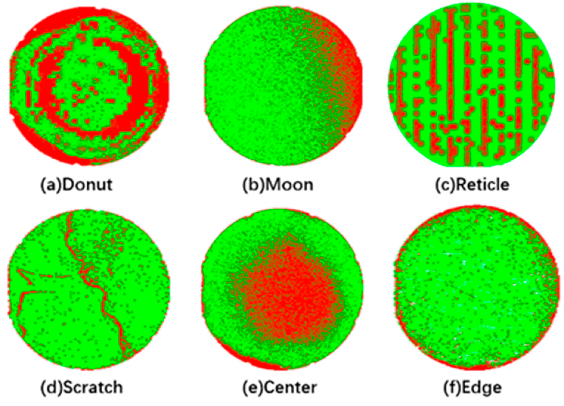
Further, after the camera takes photos of the wafer to obtain chip maps, a wafer map is able to be generated in order to locate defects visually [7]. A wafer map is used as the graphical representation of locations of the defects on the wafer. In general, defects on wafer maps are classified into two categories: the first includes random defects and the second is composed of clustered defects. Random defects are often caused by uncertain environment fluctuation. Clustered defects attract more attention from engineers and researchers since they usually provide valuable information on specific manufacturing problems. Clustered defects may form different defect patterns, e.g., scratches, rings, repeats, etc. Figure 2 shows several typical examples of wafer map patterns relating to defect-displaying diagrams. The red pixels show locations of defective chips and the green pixels are normal chips on the wafer. For example, typical patterns, like scratches, are improperly made during material handling, while edge rings are usually caused by etching problems [8].
The chip location data are important in AOI systems. The accuracy of chip positioning data directly affects the detection results of the system. If the positioning information is inaccurate, it may lead to detection errors, such as missed detection, false detection, etc. Further, accurate chip positioning information improves detection speed, thus enhancing detection efficiency. If the system knows the exact location of the chip, it can directly detect the specified location without unnecessary searches, saving time and improving detection efficiency. Additionally, chip location information can be used for product tracking and management. Through the chip positioning information, the production and testing status of each chip can be known, which facilitates production management and quality control.
There is a baseline in the x-y platform. In operating an AOI tool, when the robot arm lays a wafer on the x-y platform, it is difficult for the robot to control the angles between the chip orientation and baseline to be the same every time, resulting in errors when measuring features of different chips. This would decrease the defect recognition accuracy. It is highly desired to reduce such errors in real semiconductor manufacturing systems. This work aims to do so.

2. Literature Review

For chip defect inspection, image denoising and gray processing are conducted to improve the efficiency and effectiveness of the feature extraction for chip maps. Various features, such as shape and edge, are extracted to be compared with existing samples. Also, in the visual inspection module, there are two categories of samples: (1) samples with defects and (2) samples without defects. If there are features matching the first category of samples, it indicates that the chip is a defective one. Furthermore, in this category, these samples are classified into several subcategories representing different types of defects. If there are features matching the second category of samples, it indicates that the chip is a non-defective one. If the chip’s features do not match the second category, it means that the chip is a defective one. However, its features also do not match the first category. In this situation, it is classified into the first category and such a defect is marked as a new defect type.
Great efforts have been made on the design of AOI systems. Most studies aim to develop automatic defect detection and recognition techniques for wafer map defect patterns. For a better description, these studies can be roughly divided into three categories based on their solution goals. The first category involves constructing statistical models to monitor the defect patterns on wafer map. Ref. [9] proposes a multivariate Hotelling chart based on the number of defects and a clustering index to monitor defect patterns. Ref. [10] applies a step-down spatial randomness test to inspect abnormal wafers. The statistical models are based on assumptions of the underlying dataset’s distribution. If the dataset’s distribution is varied, the performance outputs will be negatively affected. Further, the statistical models have low flexibility. They have predetermined structures that limit their flexibility in encountering complex defect patterns. The good thing for the statistical method category is that they require few data to build the outputs. They are able to generate results based on a relatively small amount of data. They can also draw results with limited training samples, which is advantageous in scenarios where data collection is challenging.
The second category is summarized into model-based clustering methods to identify defects. These methods try to recognize defect patterns based on given shape-specific distributions of defect regions. In [11], Gaussian EM is used to detect elliptic and linear patterns, and a spherical-shell algorithm is applied to estimate ring patterns. In [12], global defects are represented by using a non-homogeneous Poisson process and local defects are denoted by using bivariate normal distribution and principal curve. Those methods in the second category are advantageous in simultaneously identifying multiple defect patterns in a single wafer map. However, it is time-consuming to estimate parameters and the recognition is only limited to simple pre-defined patterns. If a new pattern is encountered, model-based clustering methods will fail to detect it. The weakness of defining new pattern limits their defect detection capability.
The third category is defect inspection based on machine learning methods, including both unsupervised and supervised learning methods. For unsupervised learning methods, adaptive resonance theory network (ART1), self-organized map (SOM), and K-means [13,14,15,16] have been developed to construct clusters of wafer maps. When data labels and enough training samples are available, the performance of supervised learning is usually superior to unsupervised learning methods. Typical supervised leaning algorithms for defect pattern identification are supported by vector machine (SVM), K-nearest neighbors (KNN), and neural networks [17,18,19]. Machine learning models excel at learning defect patterns and features from data. By training a machine learning model on diverse datasets that include known defect types, the model can learn the characteristics of those defects and generalize that knowledge to identify similar defects in new data. Though the machine learning methods are powerful in detecting defects, they still have constraints. Machine learning models require labeled training data to learn patterns and features. The performance of machine learning is sensitive to the quality of the input data for training. For the AOI system, the data quality varies in image quality, lighting condition, camera angels, platform angles, etc. They may struggle to generalize across different manufacturing environments or adapt to changes in these conditions.
To ensure the performance of supervised learning methods, large amounts of high-quality data are required. Most current studies adopt raw wafer maps directly as inputs for supervised defect pattern recognition. However, it is inappropriate to do so due to unsatisfactory wafer map quality under practical conditions. Thus, a critical step before adopting the learning methods is feature extraction, so as to reduce the computation time and improve the accuracy. Features extracted from wafer maps significantly influence the performance of defect pattern recognition. However, in practice, it is observed that wafers have a round shape and it is hard to define the photo orientation captured by the high-resolution camera. Features are called rotation-invariant if their output results are not affected by the rotations of the input photo. For defect detection and recognition, it is desired that the same type of defect patterns with variations should have similar feature vectors for classification. This means rotation-invariant features are more preferred. Ideally, the defect patterns are identical with respect to orientation so that the samples can be classified easily.
Various rotation-invariant feature descriptors have been developed in the existing studies. One of the most popular methods is the scale-invariant feature transform (SIFT), which has illumination-, scale-, rotation-, and affine-invariant properties [20]. In [21], a rotation-invariant histogram of oriented gradients (RIHOG) is proposed to overcome the sensitivity to photo rotation of the classic histogram of oriented gradients (HOG) algorithm. Other typical examples of rotation-invariant feature descriptors are Zernike moments and speed-up robust features (SURF), etc. [22,23].
The truth is, in the x-y platform, there is a baseline. Due to the limitations of the robot arm flexibility, when the robot arm lays a wafer on the x-y platform, it is difficult for the robot to control the angles between the chip orientation and baseline to be the same every time. This leads to errors in measuring features of different chips, which causes an extreme decrease to the defect recognition accuracy. Thus, motivated by practical demands from semiconductor manufacturing requirements, this work aims to present a method to correctly extract features from the wafer map, regardless of its orientation, and an AOI system combined with this method for wafer defect pattern identification. The central array method aims to solve the angle between the baseline and the wafer placed on it. With the correction of the angle between baseline and the wafer, the chip location information is guaranteed. The correct position information ensures the detection speed enhancement and the system performance. This is important in practical semiconductor manufacturing because the AOI system ensures the production quality. Better performance in defect detection brings better quality, which means business value in practice. Improvements in detection speed mean higher efficiency. Overall, by leveraging deep learning, an AI-AOI system can perform complex visual inspections at high speed, with high accuracy, dramatically solving restrictions that current AOI systems face with positioning issues. By doing so, the semiconductor production line can reduce production costs and improve production yield.

3. A Central Array Method

In this section, how to merge chip maps to form a wafer map is introduced at first. Then, a method called the central array method is proposed to better output chip location data from the raw data input into the AOI system. Finally, this method is combined with the deep learning for better defect inspection capability.

3.1. Merging of Chip Maps

In an AOI system, to inspect defects, wafers are placed on the x-y platform. The current practical method is to apply mechanical positioning methods to locate wafers. The location information of chips is obtained based on the mechanical position coordination. However, during the AOI inspection process, the robot arm directly places a wafer onto the x-y platform. It cannot completely guarantee the arrangement of chips in the expected orientation with x-y platform. Ideally, the four sides of chips on the wafer are parallel to the x-axis or y-axis of the x-y platform. This is referred to as the chip orientation with the x-y platform being exactly matched. However, in practice, a slight angle might exist between the x-axis on the x-y platform and a side of the chips. If this angle is not considered, the location information will be incorrect. Such incorrect location information harms the subsequent defect inspection, wafer map generation, and defect classification.
The central array method is adopted in this work to get rid of the angle between the x-axis on the x-y platform and the side of the chips, such that correct position data of the chips can be obtained. Through the chip images obtained by the camera as input data, the central array method is able to merge the chip maps to form a wafer map and output the chip location data. A wafer map is a graphical representation method used in the semiconductor manufacturing process to record and display the spatial distribution of defects on the wafer. It is a two-dimensional pattern, similar to a planar projection of a wafer, where each point represents a specific location of a chip on the wafer. The chip location data are further stored and marked in the wafer map.
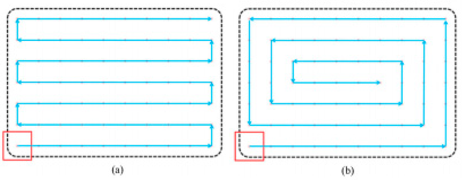
In an AOI system, the inspection process starts from when a wafer is placed on the x-y platform by using the robot arm, as illustrated in Figure 1. Then, the camera starts to take a photo of the wafer for further defect inspection. Since the wafer size is large, a single camera photo fails to provide detailed information of the wafer and the chips on it. The camera has to separately take photos of the wafer to obtain all chip photos with detailed information. There are two ways to take photos for the wafer. Figure 3 shows a traditional snake photo scan (Figure 3a) and a spiral photo scan (Figure 3b) for taking photos of chips. The red box in Figure 3 represents the starting point for scanning.
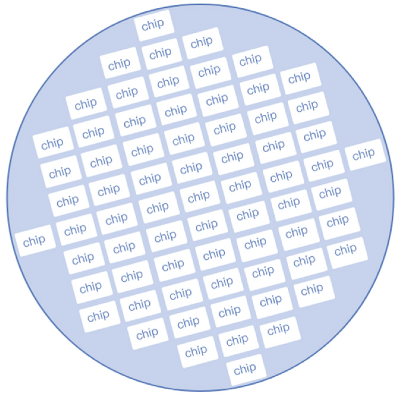
After the industry camera takes photos for the wafer, such that a number of chip photos are obtained, it is able to obtain a wafer map by merging these separate chip photos. Each image taken by the camera might contain several chips in it. An example given in Figure 4 shows that how to merge two chip photos. In the example in Figure 4, there are two chip photos: photos A and B. For better understanding and illustration, it is assumed that each photo contains nine chips. The three chips on the right side of chip photo A and the three chips on the left side of chip photo B both depict the same three chips on the wafer. If we piece together these two photos together, such that the three chips on the right side of chip photo A overlap with the three chips on the left side of chip photo B, a new chip photo can be obtained to depict more chips. In this way, by piecing together chip photos along with the direction of the photos taken repeatedly, a complete wafer map can be obtained (see Figure 5).

3.2. The Central Array Method

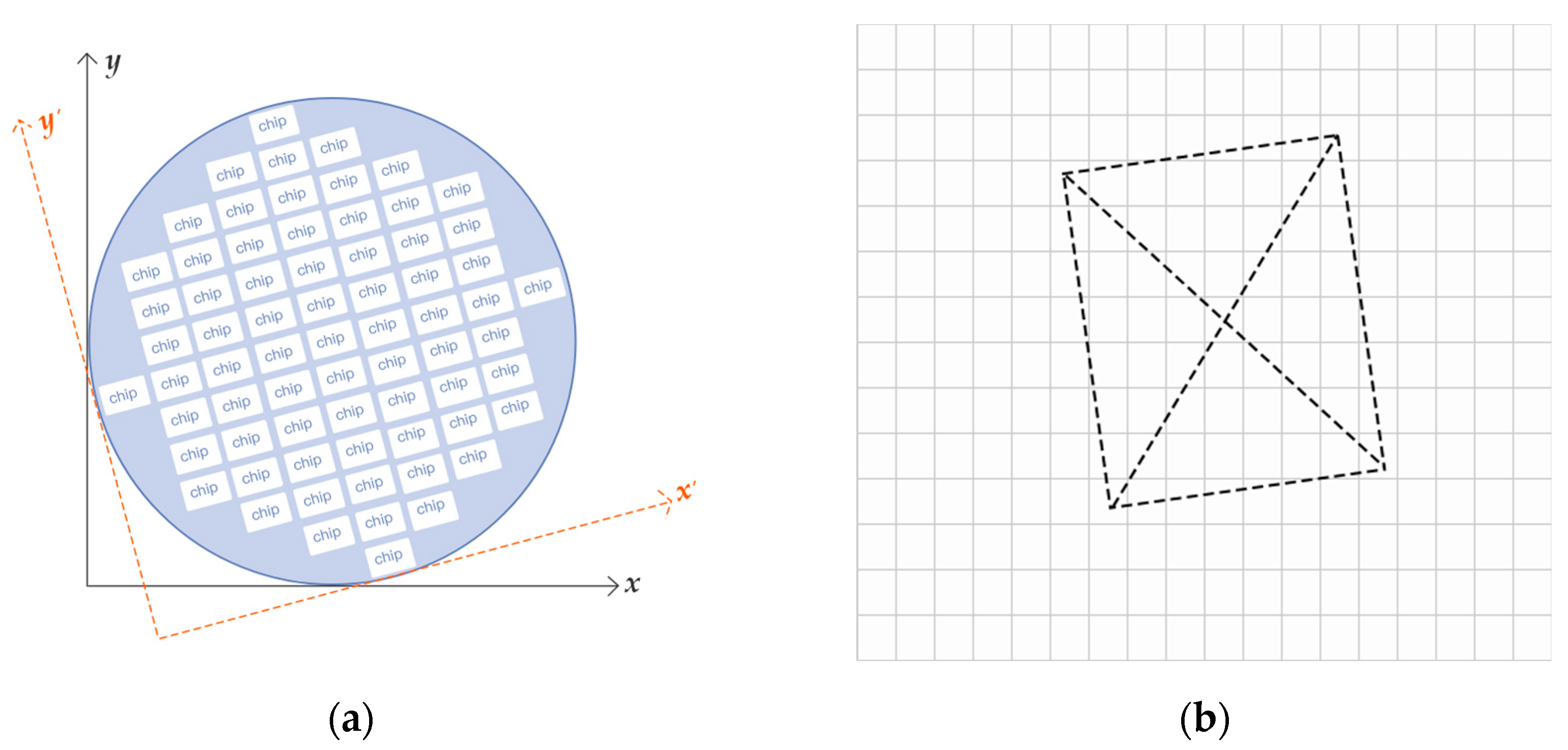
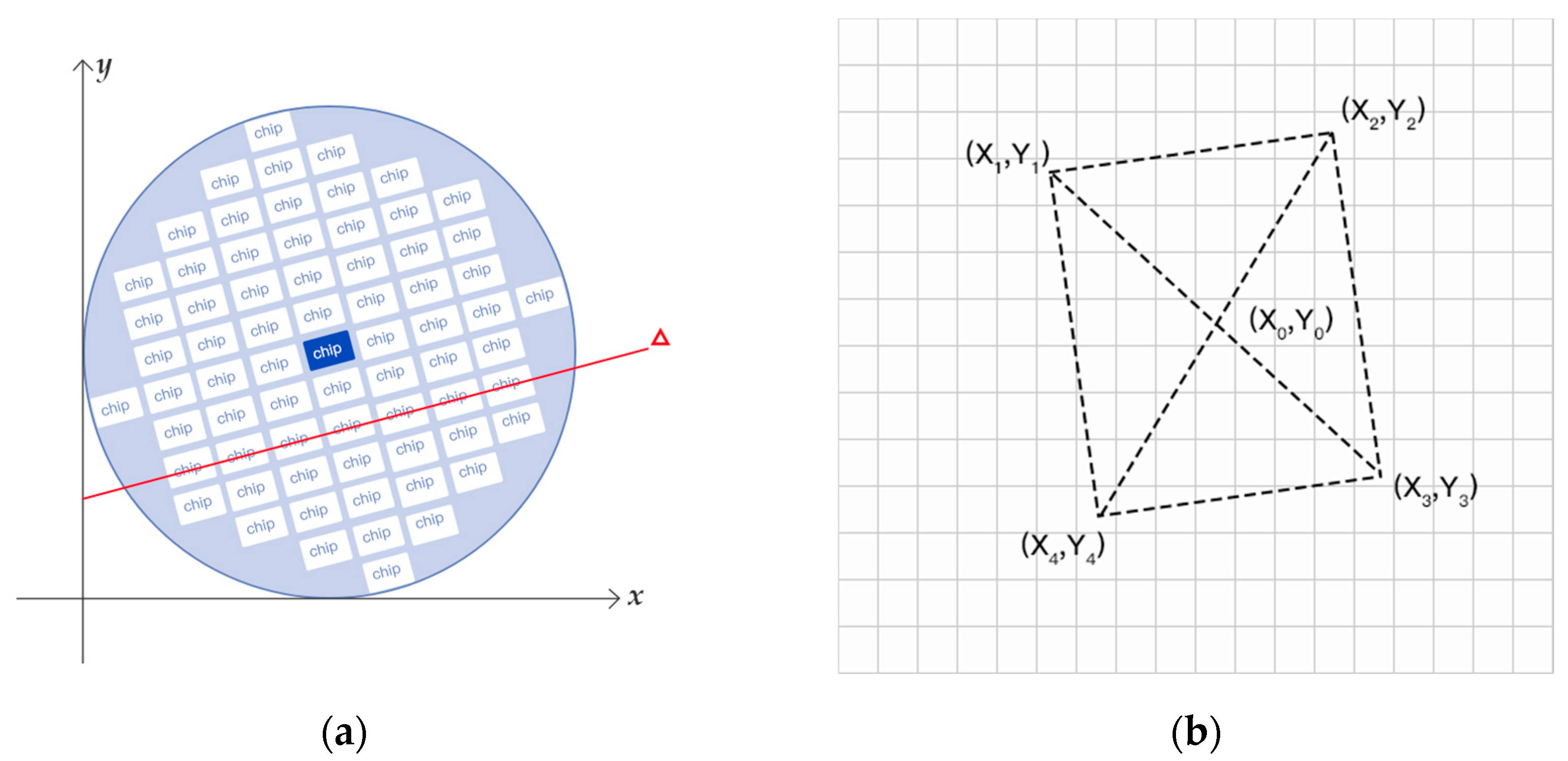
When the wafer map is obtained, the central array method is applied to locate where the chip is. To do so, a coordinate system needs to build up based on the wafer map. Notice that wafers are displayed on the x-y platform. Thus, there is an x-y coordinate system based on the mechanical system. It is marked as solid lines in Figure 6a. Meanwhile, there is an x′-y′ coordinate system based on the chips on the wafer map, called the wafer map coordinate system. The wafer map coordinate is marked as dotted lines in Figure 6a. Thus, two coordinate systems exist.
Ideally, the two coordinate systems should exactly match and overlap. However, under practical conditions, there might be an angle between the x-axis and x′-axis or the y-axis and y′-axis, i.e., an angle between two coordinate systems. To improve the defect inspection process, central array method is used to find and compensate for the angle between the two coordinate systems.
To perform the angle calculation and a rotation of the wafer map, the next step is to translate chip location on the wafer map into the location data in the x-y coordinate system. To do so, the central position of each chip represents the location information of the chip and the central positions in rows and columns build up the central array of the chips. Figure 6b is a magnified example of chip central positions. The red dots represent the central points of chips on a wafer. Each row of the chip central dots forms a line, this line is useful in the following operations.
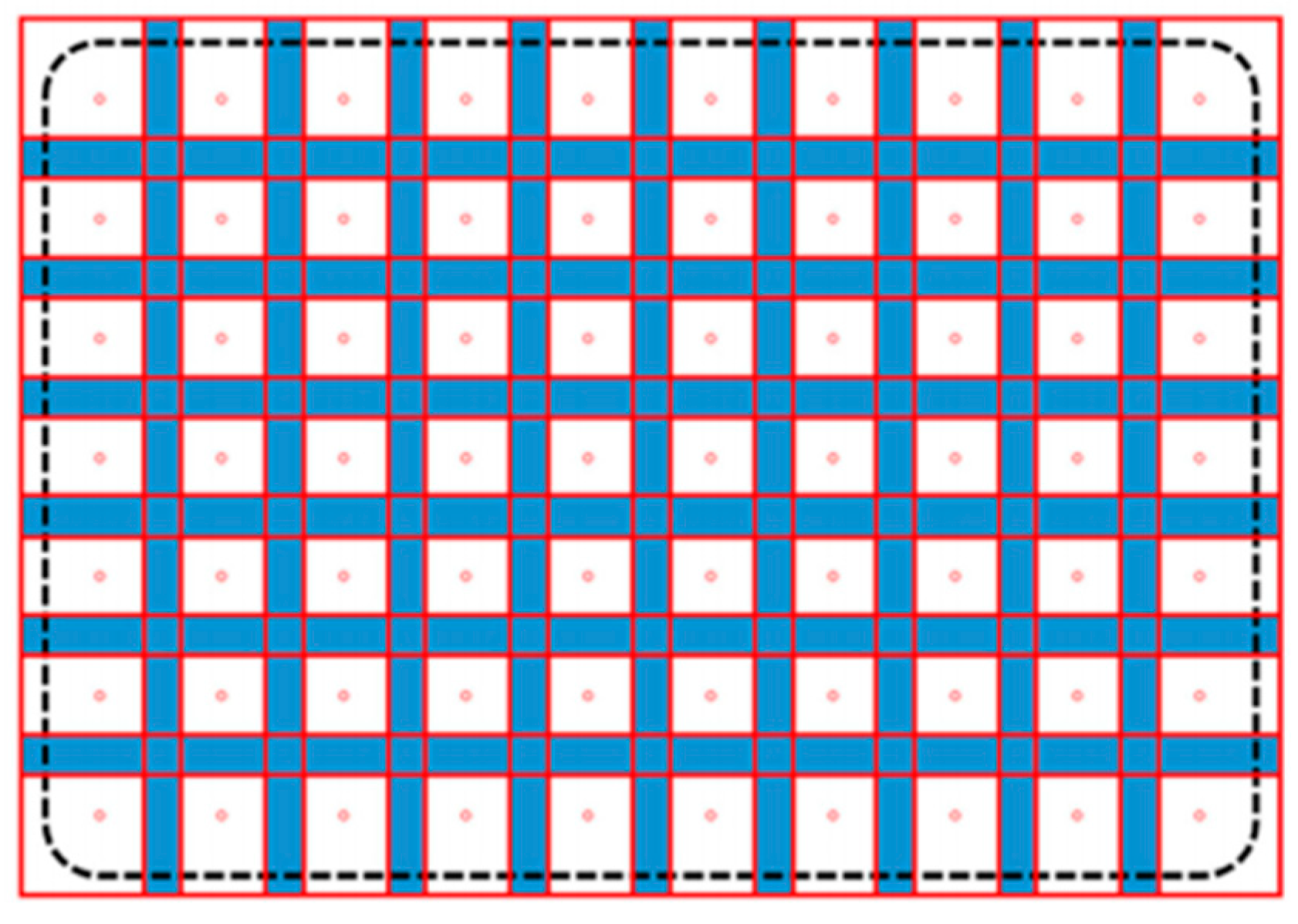
For each chip, the central points are calculated below. For any chip in the wafer map, the coordinates of its four vertices can be calculated effectively. In Figure 7, it is shown that the connection of each chip in a row builds up a line. This line is called a chip center line. Note that chip center lines are parallel to each other. The blue area represents the space between each chips, the red dots in the square chip represents its center, and the red line represents chip edge line.
Let Δ denote a line that is parallel to the chip center lines. The baseline is the x-axis in the x-y platform. In Figure 8a, the relationship between Δ and the x-axis is graphed. Then, we have the following definition.
Definition 1.
If Δ is parallel to the baseline, it is said that the wafer is placed upright on the x-y platform, and otherwise it is placed misaligned on the x-y platform.
In Figure 8b, a specific chip is magnified for better illustration. Figure 8b illustrates the central point calculation. Assume the coordinates of the four vertices of the square chip are (x1, y1), (x2, y2), (x3, y3), and (x4, y4) in the x-y coordinate system, respectively. The central point is defined as (x0, y0). Then, we have x0 = (x1 + x2)/2 = (x3 + x4)/2; y0 = (y1 + y4)/2 = (y2 + y3)/2.
For a row of chips in a wafer map, an angle might exist between the chip center line and the x-axis on the x-y platform. Let m denote the total number of chip rows in the wafer map, ni denote the number of chips of the i-th row in the wafer map, (xi,j, yi,j) denote the center coordinate of the chip in the i-th row and j-th column in the x-y coordinate system, and y = kix + bi be used to fit the line where the chip centers of the i-th row are located in the wafer map, i∈{1, 2, …, m}, j∈{1, 2, …, ni}. With the chip center coordinates in a row, the least square method is employed to fit ki and bi. Then, we have
k i = n i j = 1 n i x i , j y i , j j = 1 n i x i , j j = 1 n i y i , j n i j = 1 n i x i , j 2 ( j = 1 n i x i , j ) 2 b i = j = 1 n i y i , j n i k i j = 1 n i x i , j n i , i { 1 ,   2 ,   ,   m }
By using (1), for each row of chip centers in the wafer map, y = kix + bi can be obtained, i∈{1, 2, …, m}. Due to the unavoidable error in merging the chip photos, it is possible that the lines obtained by (1) are not parallel to each other in the wafer map. Let κ denote the slope of Δ. Then, we have
κ = ( i = 1 m k i ) / m
By using (2), an average slope can be obtained. In the x-y coordinate system, the slope of the baseline is zero. According to Definition 1, if κ is not approximately equal to 0, the wafer is misaligned on the x-y platform. In this case, the features extracted from the wafer map undergo deformation, such that they could not be compared with the samples correctly. Thus, we try to rotate the wafer map, such that κ is approximately equal to 0. Let θ denote the angle between the positive half of the x-axis and Δ, measured counterclockwise from the x-axis. Then, we have
θ = arctan(κ)
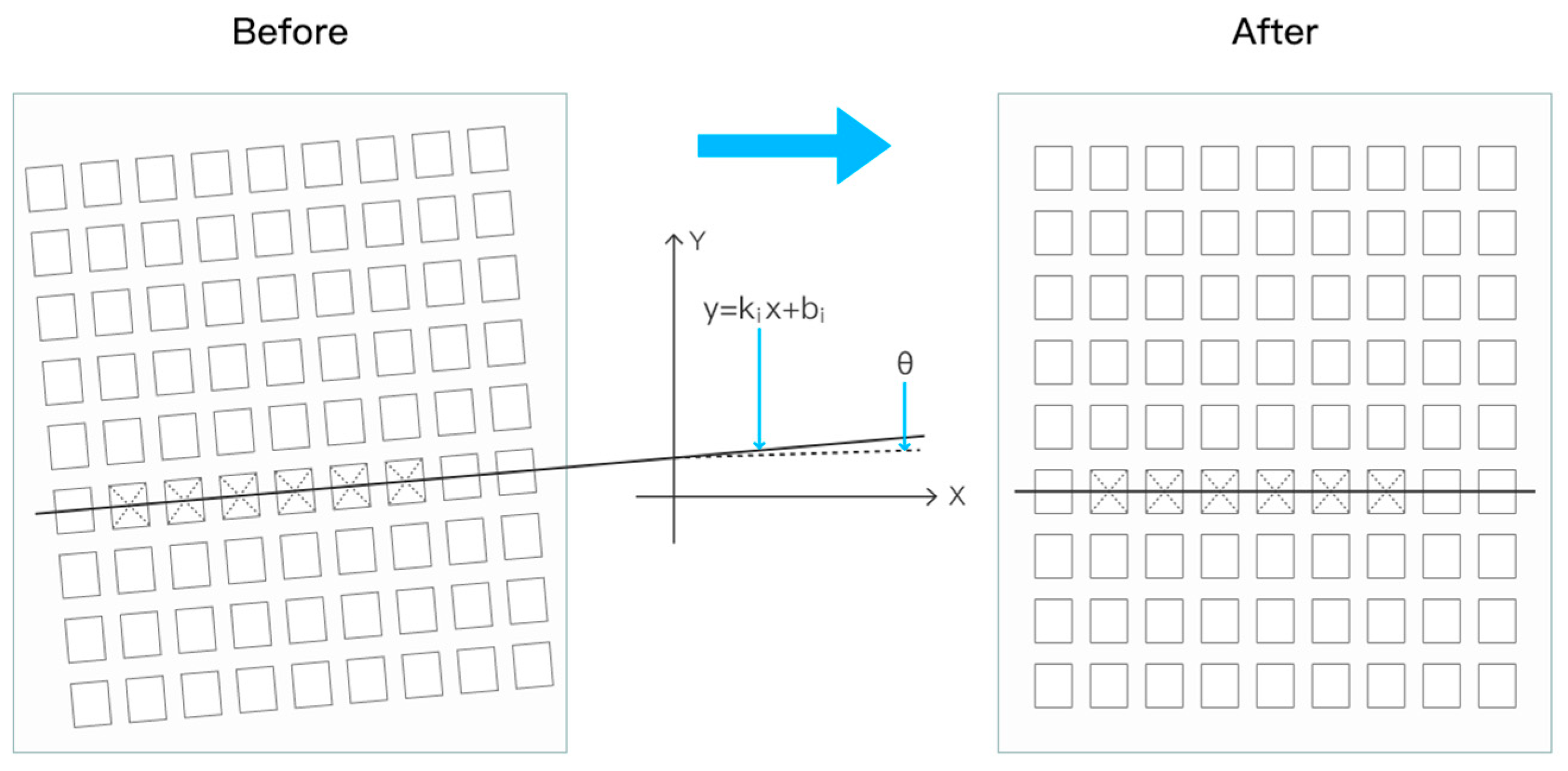
By using (3), θ can be obtained. After rotating the wafer map θ clockwise, κ is close to 0. Further, for locating each chip in the rotated wafer map efficiently, it is necessary to obtain the new coordinates of the chip center in the rotated wafer map. The rotation process is graphed in Figure 9 for better understanding. In Figure 9, the chip central line is parallel with the x-axis after rotation.
Let Θ represent the radian measure corresponding to θ. Next, according to the following equation, Θ can be calculated.
Θ = θ × (π/180)
With the origin as the rotation center, the rotation matrix can be obtained by (5).
R = c o s   Θ s i n   Θ s i n   Θ c o s   Θ
Then, for the coordinate (x, y) in the x-y platform before rotation, the new coordinate (x′, y′) after rotation can be obtained by (6)
x y = c o s   Θ s i n   Θ s i n   Θ c o s   Θ x y
In this way, all new coordinates in the rotated wafer map can be calculated efficiently. After the rotation of the wafer map, the two coordinate systems are merged into the same coordinate system, such that positions of the chips in the x-y coordination system can be obtained by considering the angle between the center lines and x-axis of the x-y platform.

3.3. Implementation of Deep Learning in the AOI System

The central array method outputs two kinds of important data, the positioning data for each segmented chip on the wafer and the whole wafer map. The positioning data boost the chip image operation while the wafer map lays the foundation for data training.
Apart from the theory of the central array method, the implementation of this method in practice is needed. To implement the central array method and deep learning method in an AOI system to further improve the output performance, this paper designs an AI-based AOI system (AI-AOI system). The implementation of the central array method workflow mechanism is described in Figure 10.
To better inspect chip defects after the wafer map rotation, such that each chip in the wafer map can be located efficiently, a deep learning method is implemented in the AOI system. There is an online training and an offline training in the deep learning method. Convolutional neural networks (CNNs) are pivotal in fields requiring complex pattern recognition and feature extraction. CNNs adopt a unique architecture that employs local connections and weight sharing, enabling them to efficiently capture local features, such as edges and textures in data. Such a specialized structure allows CNNs to reduce the number of parameters, significantly enhancing their ability to learn hierarchical feature representations from high-dimensional data. Thus, CNNs are implemented to record data and classify defects in this work.
For the offline training, CNNs are trained with a fixed and pre-collected dataset, which contains several defect categories with corresponding features represented by numerical data. Figure 10 shows the complete process of the offline training of CNN in the AOI. According to the central array method, high-quality chip maps can be obtained. Through noise reduction, resizing, normalization, and grayscale conversion, these high-quality chip maps are transformed into a numerical array representation, and then stored in the sample set. After all chip maps are represented as numerical data, the training of the CNN model starts to be performed. According to data labeled with a corresponding category, the CNN model is trained to predict these labels accurately by adjusting its parameters based on the differences between its predictions and the actual labels.
Notice that, with the rapid development of chip design, more and more unclassified features representing the unqualified chips are emerging. To train the network to accommodate these new categories in time, online training is required by the CNN model. In this training mode, there is a category representing the unidentified features. When a set of undiscovered features emerge, it is classified into the category representing the unidentified features. By replacing the output layer and freezing some initial layers, the CNN model is updated to classify these new features into a new category and keep prediction accuracy for other type of defects.

4. Experiments

To demonstrate the performance of the proposed AI-based AOI system, experiments were conducted with the practical parameters.
In practice, there are four common types of wafer recipes, which are called S-B-K, S-G-K, S-B-M, and S-G-M, respectively. Wafers with these wafer recipes are required to be detected in the AOI system. Table 1 shows the average time needed for the AI-based AOI system and current AOI system to detect wafers. Assume that there are four batches of wafers with the corresponding wafer recipes. As shown in Table 1, for each type of recipe, the average detection time of AI-based AOI system is 15% less than that of the current AOI system. This implies that the proposed method has a higher efficiency than the convention method.
In the experiments, there was a batch of qualified wafers. To test the chip quality inspection accuracy of the AOI systems, the batch of wafers was sent to the AOI systems for quality detection. Each wafer detected by the AOI systems can be classified into the following two cases:
Case 1: It is qualified in fact, and the inspection results of the AOI system show that it is qualified. Let TP denote the total number of wafers classified into this case.
Case 2: It is qualified in fact, and the inspection results of the AOI show that it is unqualified. Let FN denote the total number of wafers classified into this case.
The yield rate is also known as ‘pass rate’ in semiconductor manufacturing. It is one of the product quality indicators, referring to the percentage of qualified products in all processed products. It is calculated by all quality-passed chips divided by all chips.
Y R = T P T P + F N × 100 %
Table 2 shows the YRs of two types of AOI systems detecting the quality of the batch of wafers. Notice that, for each type of wafer, the overall yield rate obtained by the AI-based AOI system increases by 1% when comparing with the current AOI system. Further, the overall YTs of the AI-based AOI system all improve to more than 98%. This indicates that the central array method is beneficial to the improvement of the chip quality inspection accuracy.
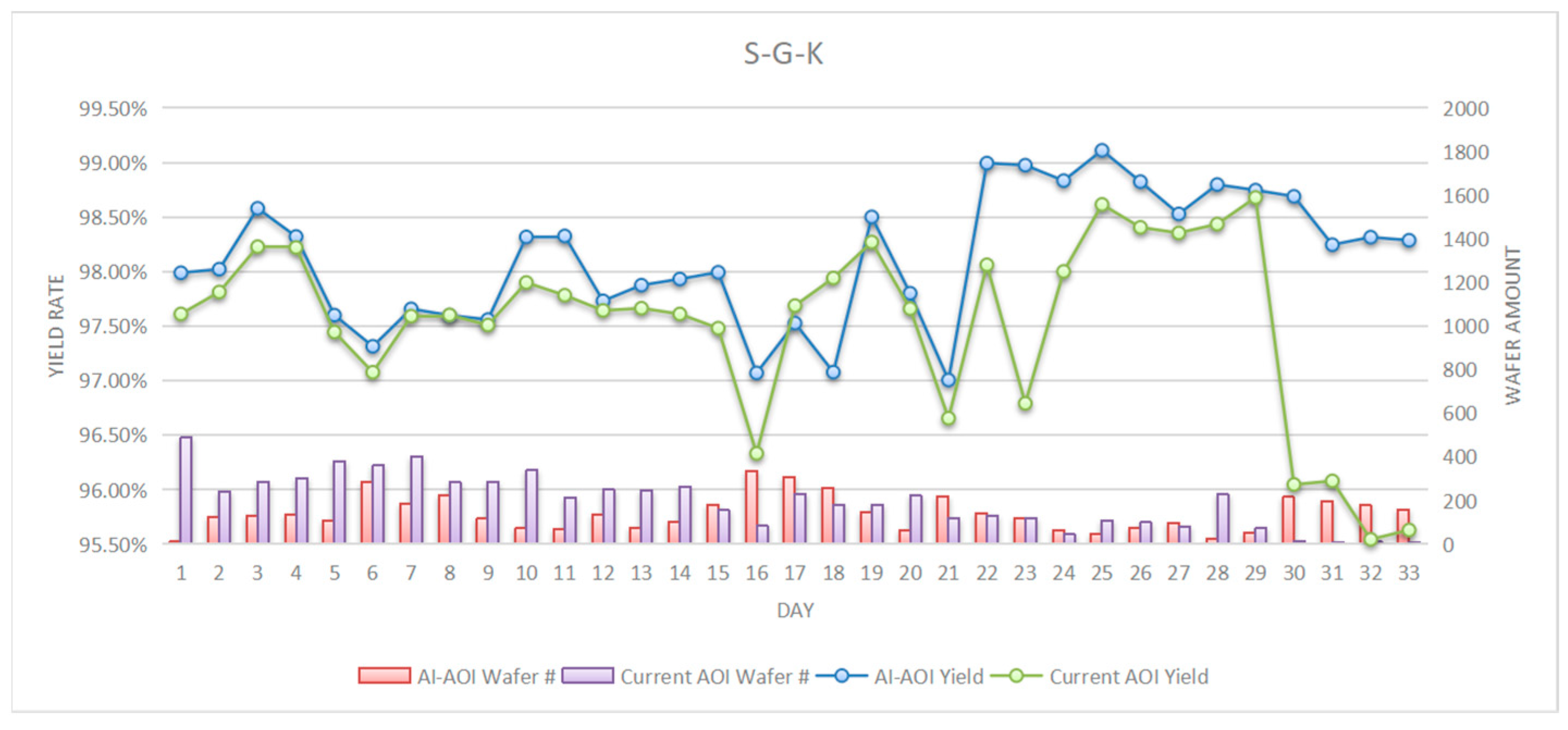
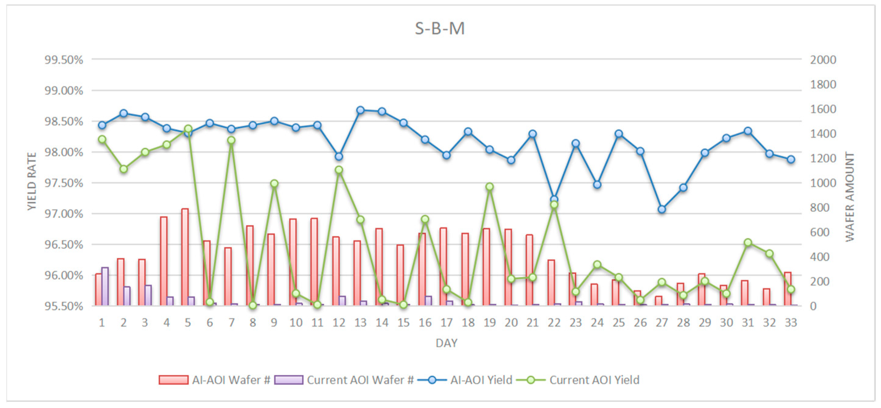
Figure 11, Figure 12, Figure 13 and Figure 14 show the detailed detection success rate for the four tested wafer recipes. It reveals the designed AI-based AOI system outperforms the current AOI system. For wafer recipe S-B-K in Figure 11, the maximum and minimum yield reach 99.06% and 98.01% for the AI-based AOI system, respectively, while in the meantime, the current AOI system only reaches 98.76% and 97.62% for maximum and minimum yield, respectively. Through the test, the average yield for the AI-based AOI system reaches 98.54%, while the current AOI system obtains 98.19% yield. According to the graph, the AI-AOI system yield is mostly better than the current AOI system. Further, the yield rate is smoother compared with current AOI system.
Figure 12 shows the yield rate for wafer recipe S-G-K. Both AOI systems perform a wide yield range compared with wafer recipe S-G-K. The wafer panels applied in this recipe are smaller than those of the S-B-K recipe. Further, the yield rate has a wider difference range. Nevertheless, the minimum yield for the AI-based AOI system remains above 97%. The average yield for the AI-based AOI system is 98.06% compared with 97.11% for the current AOI system. As for the very last four days in the test, the AI-based AOI system can still maintain its yield rate, while the current AOI system fails to do so.
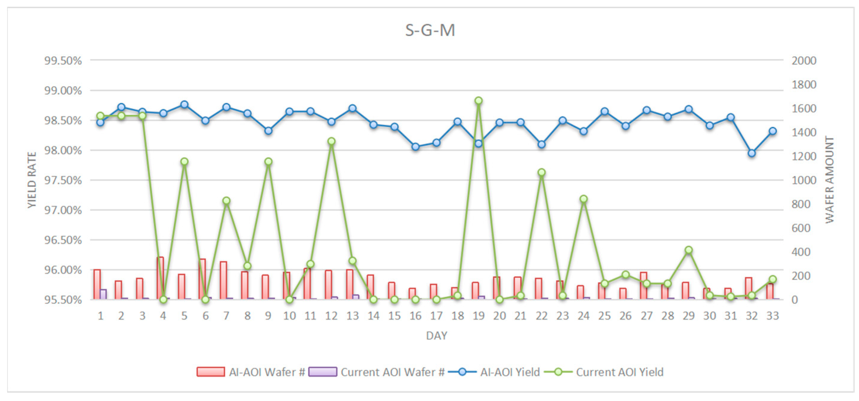
As for the other two wafer recipes (S-B-M and S-G-M), test results reveal the same trend for the production yield—the AI-AOI system provides a stable yield compared with the current AOI system, which fluctuates severely since the yield difference is relatively large. The AI-based AOI system yield trend is stable, with more wafer chip inspected. The average yield values for wafer recipe S-B-M and S-G-M under the AI-based AOI system reach 97.87% and 98.35%, respectively. In total, 8589 pieces of wafers were applied for the inspection test.

5. Conclusions

The AOI system is a core software system in the manufacturing quality assurance field. In this article, a central array method is proposed to improve the wafer chip location technique. In this way, the captured photo is better positioned and the influence caused by an unexpected positioning angle with x-y platform can be eliminated. Further, the central array method is integrated with the AOI system and upgraded into the AI-based AOI system based on deep learning methodologies. The AOI system integrated with deep learning enables the transformed photo to be used for continuous data training and data inference. Such an AI-based AOI system can improve AOI system outputs. The detection speed is increased by 15%, on average, while the AOI system yield rate increases 1% in general, with less difference. The current AOI system encounters 5% difference, while the designed AI-AOI system difference is within 2%. The experiments show that the proposed method can make improvements in the yield and inspection speed. Future work will focus on the application of the proposed AI-based AOI system in more production lines so as to save labor resources.

Author Contributions

Conceptualization, H.F. and S.Z.; methodology, H.F. and S.Z.; validation, H.F. and Y.L.; formal analysis, H.F., L.B. and J.L.; investigation, H.F. and S.Z.; resources, L.B. and C.P.; data curation, H.F., Y.L. and J.L.; writing—original draft preparation, H.F. and S.Z.; writing—review and editing, L.B.; supervision, S.Z. and L.B.; project administration, L.B. and C.P.; funding acquisition, L.B. and C.P. All authors have read and agreed to the published version of the manuscript.

Funding

This research was funded in part by Science and Technology development fund (FDCT), Macau SAR (file Nos. 0018/2021/A1, 0027/2022/AGJ, 0083/2021/A2, 0015/2020/AMJ and 0011/2023/RIA1), in party by Natural Science Foundation of Guangdong Province (2023A0505020007), and in part by the National Natural Science Foundation (72161019), China.

Data Availability Statement

Data is contained within the article.

Conflicts of Interest

Author Jie Li was employed by the company IKAS Industries Company, Ltd., Chongqing 400000, China. The remaining authors declare that the research was conducted in the absence of any commercial or financial relationships that could be construed as a potential conflict of interest.

References

  1. Kim, J.; Lee, Y.; Kim, H. Detection and clustering of mixed-type defect patterns in wafer bin maps. IISE Trans. 2018, 50, 99–111. [Google Scholar] [CrossRef]
  2. Jin, C.; Na, H.; Piao, M.; Pok, G.; Ryu, K. A novel DBSCAN-based defect pattern detection and classification framework for wafer bin map. IEEE Trans. Semicond. Manuf. 2019, 32, 286–292. [Google Scholar]
  3. Qiao, Y.; Wu, N.; Zhou, M. Real-time scheduling of single-arm cluster tools subject to residency time constraints and bounded activity time variation. IEEE Trans. Autom. Sci. Eng. 2012, 9, 564–577. [Google Scholar] [CrossRef]
  4. Qiao, Y.; Wu, N.; Zhou, M. A Petri net–based novel scheduling approach and its cycle time analysis for dual-arm cluster tools with wafer revisiting. IEEE Trans. Semicond. Manuf. 2013, 26, 100–110. [Google Scholar] [CrossRef]
  5. Song, T.; Qiao, Y.; He, Y.; Wu, N.; Li, Z.; Liu, B. Dual-arm cluster tool scheduling for reentrant wafer flows. Electronics 2023, 12, 2411. [Google Scholar] [CrossRef]
  6. Zhu, Q.; Qiao, Y.; Wu, N.; Hou, Y. Post-processing time-aware optimal scheduling of single robotic cluster tools. IEEE CAA J. Autom. Sin. 2020, 7, 597–605. [Google Scholar] [CrossRef]
  7. Adly, F.; Yoo, P.; Muhaidat, S.; Al-Hammadi, Y.; Lee, U.; Ismail, M. Randomized general regression network for identification of defect patterns in semiconductor wafer maps. IEEE Trans. Semicond. Manuf. 2015, 28, 145–152. [Google Scholar] [CrossRef]
  8. Yu, J.; Lu, X. Wafer map defect detection and recognition using joint local and nonlocal linear discriminant analysis. IEEE Trans. Semicond. Manuf. 2016, 29, 33–43. [Google Scholar] [CrossRef]
  9. Tong, L.-I.; Wang, C.-H.; Huang, C.-L. Monitoring defects in IC fabrication using a hotelling T2 control chart. IEEE Trans. Semicond. Manuf. 2005, 18, 140–147. [Google Scholar] [CrossRef]
  10. Kim, B.; Jeong, Y.-S.; Tong, S.; Chang, I.-K.; Jeong, M.-K. Step-down spatial randomness test for detecting abnormalities in DRAM wafers with multiple spatial maps. IEEE Trans. Semicond. Manuf. 2016, 29, 57–65. [Google Scholar] [CrossRef]
  11. Wang, C.-H.; Kuo, W.; Bensmail, H. Detection and classification of defect patterns on semiconductor wafers. IIE Trans. 2006, 38, 1059–1068. [Google Scholar] [CrossRef]
  12. Hwang, J.; Kuo, W. Model-based clustering for integrated circuit yield enhancement. Eur. J. Oper. Res. 2005, 178, 143–153. [Google Scholar] [CrossRef]
  13. Chien, C.-F.; Hsu, S.-C.; Chen, Y.-J. A system for online detection and classification of wafer bin map defect patterns for manufacturing intelligence. Int. J. Prod. Res. 2013, 51, 2324–2338. [Google Scholar] [CrossRef]
  14. Lee, J.; Yu, S.; Park, S. Design of intelligent data sampling methodology based on data mining. IEEE Trans. Robot. Autom. 2001, 17, 637–649. [Google Scholar] [CrossRef]
  15. Wang, C.-H.; Wang, S.-J.; Lee, W.-D. Automatic identification of spatial defect patterns for semiconductor manufacturing. Int. J. Prod. Res. 2006, 44, 5169–5185. [Google Scholar] [CrossRef]
  16. Chien, C.-F.; Wang, W.-C.; Cheng, J.-C. Data mining for yield enhancement in semiconductor manufacturing and an empirical study. Expert Syst. Appl. 2007, 33, 192–198. [Google Scholar] [CrossRef]
  17. Wu, M.-J.; Jang, J.-S.; Chen, J.-L. Wafer map failure pattern recognition and similarity ranking for large-scale data sets. IEEE Trans. Semicond. Manuf. 2015, 28, 1–12. [Google Scholar]
  18. Kim, B.; Jeong, Y.-S.; Tong, S.H.; Chang, I.-K.; Jeongyoung, M.-K. A regularized singular value decomposition-based approach for failure pattern classification on fail bit map in a DRAM wafer. IEEE Trans. Semicond. Manuf. 2015, 28, 41–49. [Google Scholar]
  19. Kyeong, K.; Kim, H. Classification of mixed-type defect patterns in wafer bin maps using convolutional neural networks. IEEE Trans. Semicond. Manuf. 2018, 31, 395–402. [Google Scholar] [CrossRef]
  20. Lowe, D. Distinctive image features from scale-invariant key-points. Int. J. Comput. Vis. 2004, 60, 91–110. [Google Scholar] [CrossRef]
  21. Cheon, M.-K.; Lee, W.-J.; Hyun, C.-H.; Park, M. Rotation invariant histogram of oriented gradients. Int. J. Fuzzy Log. Intell. Syst. 2011, 11, 293–298. [Google Scholar] [CrossRef]
  22. Khotanzad, A.; Hong, Y. Invariant image recognition by Zernike moments. IEEE Trans. Pattern Anal. Mach. Intell. 1990, 12, 489–497. [Google Scholar] [CrossRef]
  23. Bay, H.; Ess, A.; Tuytelaars, T.; Van Gool, L. Speeded-up robust features (SURF). Comput. Vis. Image Underst. 2008, 110, 346–359. [Google Scholar] [CrossRef]
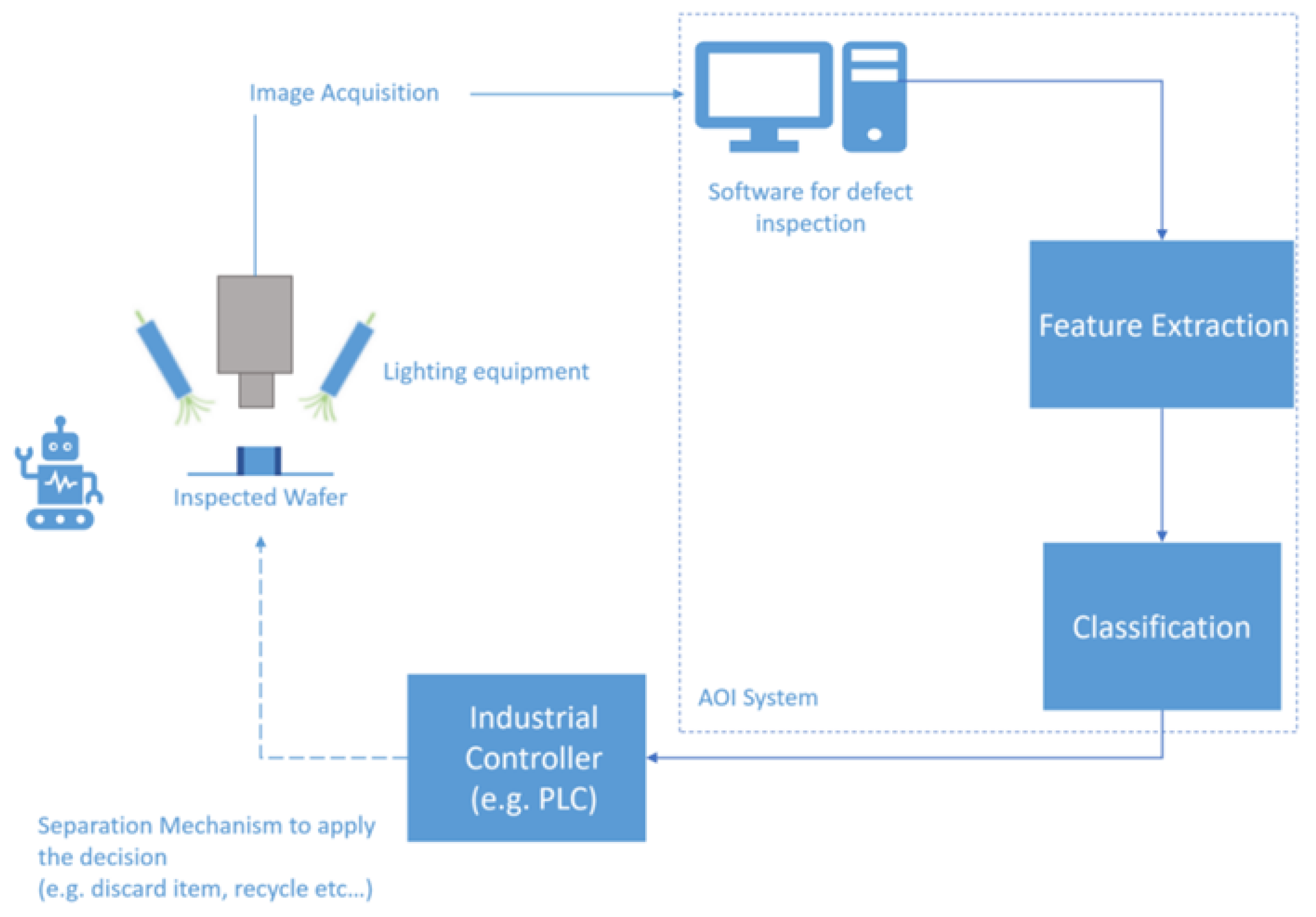
Figure 1. Logical diagram of the AOI system.
Electronics 13 01070 g001
Figure 2. Typical examples of wafer defect patterns.
Electronics 13 01070 g002
Figure 3. Camera scanning path.
Electronics 13 01070 g003
Figure 4. An example to show the merging of two chip photos.
Electronics 13 01070 g004
Figure 5. A completed wafer map.
Electronics 13 01070 g005
Figure 6. (a) Wafer map coordinate system; (b) magnified chip central position.
Electronics 13 01070 g006
Figure 7. Central representation of chips on a wafer.
Electronics 13 01070 g007
Figure 8. (a) Chip central line in x-y coordinates; (b) magnified chip central calculation.
Electronics 13 01070 g008
Figure 9. Rotation of the wafer map image.
Electronics 13 01070 g009
Figure 10. Flowchart of deep learning with AOI system work mechanism.
Electronics 13 01070 g010
Figure 11. Yield performance for wafer recipe S-B-K.
Electronics 13 01070 g011
Figure 12. Yield performance for wafer recipe S-G-K.
Electronics 13 01070 g012
Figure 13. Yield performance for wafer recipe S-B-M.
Electronics 13 01070 g013
Figure 14. Yield performance for wafer recipe S-G-M.
Electronics 13 01070 g014
Table 1. Detection speed of two AOI systems.
System TypeWafer RecipeAverage Detection Time
AI-based AOI systemS-B-K0:04:03
S-G-K0:04:20
S-B-M0:03:39
S-G-M0:03:56
Current AOI systemS-B-K0:04:46
S-G-K0:05:06
S-B-M0:04:17
S-G-M0:04:39
Table 2. Yield rate comparison of two types of AOI system.
System TypeWafer RecipeMinimum YRMaximum YROverall YR
AI-based AOI systemS-B-K98.01%99.06%98.54%
S-G-K97.01%99.11%98.06%
S-B-M97.07%98.68%97.87%
S-G-M97.95%98.76%98.35%
Current AOI systemS-B-K97.62%98.76%98.19%
S-G-K95.54%98.68%97.11%
S-B-M95.51%98.37%96.94%
S-G-M95.50%98.83%97.16%
Disclaimer/Publisher’s Note: The statements, opinions and data contained in all publications are solely those of the individual author(s) and contributor(s) and not of MDPI and/or the editor(s). MDPI and/or the editor(s) disclaim responsibility for any injury to people or property resulting from any ideas, methods, instructions or products referred to in the content.