Article

A Novel Modular Sigma DC/DC Converter with a Wide Input Voltage Range

1
College of Electrical Engineering, Zhejiang University, Hangzhou 310027, China
2
Shanxi Key Lab of Power System Operation and Control, Taiyuan University of Technology, Taiyuan 030002, China
*
Author to whom correspondence should be addressed.
Electronics 2024, 13(5), 995; https://doi.org/10.3390/electronics13050995
Submission received: 1 February 2024 / Revised: 29 February 2024 / Accepted: 29 February 2024 / Published: 6 March 2024
(This article belongs to the Section Industrial Electronics)

Abstract

:
A modular Sigma DC/DC converter with wide input voltage range is proposed in this paper. The proposed converter is combined with a traditional LLC converter and two multi-resonant converters via Sigma architecture. Among them, the traditional LLC converter operates as a DC transformer (DCX) at resonant frequency to achieve maximum efficiency. Meanwhile, one of the multi-resonant converters, the DC to DC (D2D) part of the Sigma structure, is responsible for voltage regulation over a wide input voltage range. In addition, the other multi-resonant converter has two operation modes, including DCX and D2D. When it operates in the DCX mode, the Sigma converter has better performance and higher efficiency. When it operates in the D2D mode, the Sigma converter can handle a wider input voltage range. For each submodule, the operation principle and characteristics of the proposed Sigma converter are analyzed in detail. In addition, some key points of the parameter design for each part are also demonstrated. Finally, an experimental prototype with an input voltage of 540~1100 V is built to verify the effectiveness of the proposed converter.

1. Introduction

With the increase of photovoltaic generation capacity and electric vehicle load capacity, higher DC bus voltage level is considered to be a promising solution to reduce body weight and improve system efficiency [1]. Photovoltaic panels in series connection are often accompanied by the requirement for DC/DC converters with a wide input voltage range [2]. Furthermore, in new electrical vehicle applications, the on-board DC/DC converter is responsible for converting the high voltage of the power battery (generally 200~750 V) to the low voltage of 24 V or 48 V; so, the on-board DC/DC converters still need to have the ability to regulate the output voltage with a wide input voltage range [3,4].
As an important part of energy conversion, a DC/DC converter is an indispensable electronic device that is widely used in various applications. Unfortunately, there are many factors limiting the use of DC/DC converters in high-voltage applications, and one of them is power devices [5]. It is difficult for the rated voltage of a single power device to meet the high voltage requirement. Meanwhile, it is not feasible to connect the power devices in series to adapt to higher voltages because it is difficult to achieve voltage equalization and drive synchronization [6].
Input-series output-parallel (ISOP) converters have been proposed to overcome the limitations of DC/DC converters in high-voltage applications [7,8,9,10]. The voltage stress of power devices can be reduced with input terminals arranged in series connection. The submodules of an ISOP converter mainly include two types: one is a dual-active bridge (DAB) converter [7,8], and the other is a resonant converter [9,10]. However, these submodules of the ISOP converter have the same voltage and current-sharing control, which may lead to low efficiency under light-load and voltage regulation conditions.
The concept of the Sigma converter, as a type of special ISOP converter, was proposed by Dr. Xu [11]. The Sigma converter is composed of an unregulated converter and a regulated converter. The unregulated converter acts as a DC transformer (DCX), and the regulated converter acts as a DC/DC (D2D) converter, as shown in Figure 1. Based on this concept, which is different from the normal ISOP structure with an identical submodule, a hybrid ISOP converter consists of a DAB converter as a D2D converter and several series resonant converters (SRCs) as a DCX [12]. An LLC converter can also be used as a DCX to improve system performance [13,14].
In order to adapt to wide input voltage range applications, a series of measures are implemented on LLC-based resonant DC/DC converters. A variable frequency with phase-shift modulation has been proposed for wide input voltage range applications in [15], and a variable frequency with a duty-cycle-modulated control method has been used to improve the LLC light load efficiency for a wide input voltage range in [16]. Furthermore, switching between full-bridge and half-bridge is achieved by controlling the opening and closing of the switch tubes, thereby expanding the voltage gain [17]. Similarly, a dual-bridge LLC resonant converter is also proposed for wide input voltage range applications in [18]. Another transformer winding can also be introduced to change the system structure to adapt to the large voltage gain. The new transformer winding can be integrated into a single LLC with an LC antiresonant circuit in a parallel branch [19], as well as with the previous winding as two split resonant branches for wide-input-range applications [20]. In addition to the above measures, changing the structure of the resonant tank is also a feasible method. A notch filter can be introduced into the resonant tank to make the voltage gain decrease rapidly with an increase in frequency so as to achieve wider gain regulation [21,22,23]. The results show that these multi-resonant converters cannot only broaden the voltage gain but also transmit the fundamental and third harmonics so as to improve the efficiency.
Based on the above analysis, a modular Sigma ISOP DC/DC converter for high and wide input voltage applications is proposed in this paper. The Sigma converter consists of a traditional LLC converter as a DCX and two novel multi-resonant converters as D2D. The DCX is designed to operate at its resonant frequency to deliver as much power as possible, and the D2D is designed to regulate the output voltage with a wide input voltage range. Moreover, in order to improve system performance, one of the D2D converters can change its operation mode from D2D to DCX based on the input voltage conditions.
The rest of this paper is organized as follows. Section 2 introduces the topology of the proposed Sigma converter and analyzes the characteristics of each submodule. The operation principle of the proposed Sigma DC/DC converter is analyzed in Section 3. Some key points of the parameter design are given in Section 4. Section 5 shows the experimental results. Finally, Section 6 concludes this paper.

2. Topology of Proposed Modular Sigma DC/DC Converter

The topology of the proposed Sigma converter is shown in Figure 2. The Sigma converter combines two multi-resonant converters with an LLC–DCX converter through an input-series output-parallel (ISOP) structure. Among them, the two multi-resonant converters share the same parameters. Figure 2a shows the overall structure. The input voltage of the Sigma converter (Vin) includes three parts, i.e., VinL, VinM1, and VinM2. They are the input voltages of the LLC–DCX converter, multi-resonant converter #1, and multi-resonant converter #2, respectively. Moreover, Iin, Io, and Vo are the input current, output current, and output voltage, respectively, of the Sigma converter.

2.1. LLC–DCX Converter

Figure 2b shows an LLC–DCX converter whose operating frequency is fixed at a resonant frequency to increase system efficiency. Thus, the LLC–DCX converter is equivalent to an unregulated DC transformer. Power switches S1~S4 are driven by switching signals with 50% duty cycle. DL1~DL4 are diodes in the rectifier circuit, and CoL is an output rectifier capacitor. LrL, LmL,, and CrL are the resonant inductor, magnetizing inductor, and resonant capacitor, respectively. In addition, iLrL, iLmL,, and isL represent the resonant current, magnetizing inductor current, and secondary side current, respectively. nL is turns ratio of transformer TL.
Since the LLC converter operates in the DCX mode, it is assumed that the relation between VinL and Vo can be expressed as
V i n L = n L V o

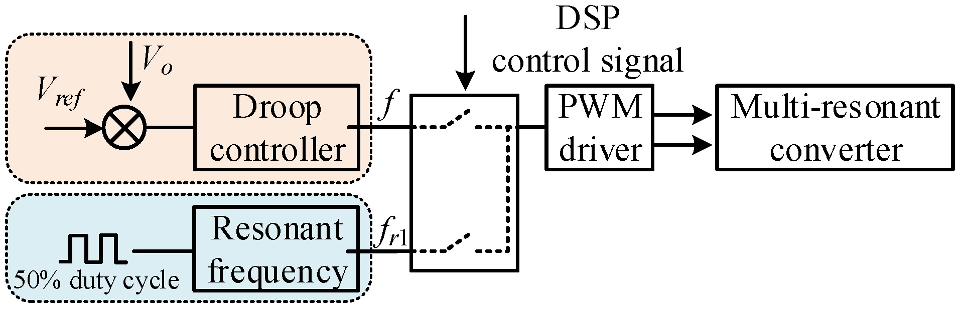
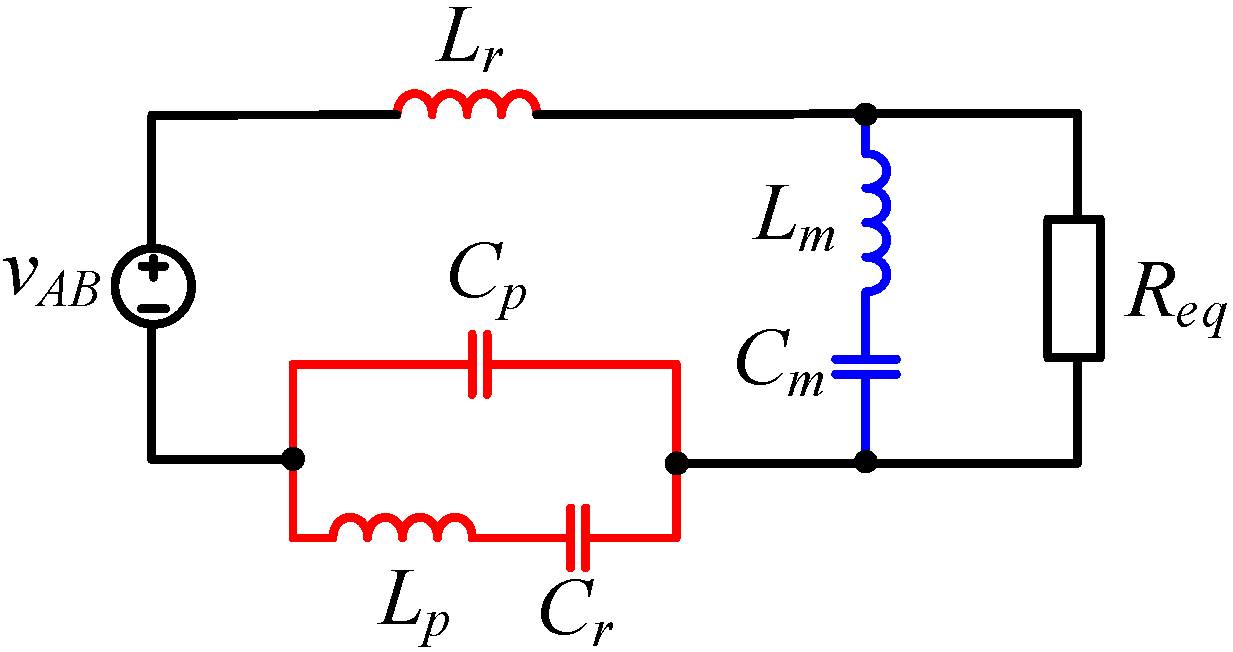
2.2. Multi-Resonant Converter

In addition to LLC–DCX, there is also the D2D part in the Sigma structure to regulate voltage with a wide input voltage range, so a type of wide-input-voltage multi-resonant converter is introduced as the D2D converter, as shown in Figure 2c. Different from traditional LLC converters, a notch filter, composed of Cp, Lp, Cr, and Cr, is introduced, and the excitation branch is changed into Lm and Cm in series.
The topology of the multi-resonant converter can be simplified, as shown in Figure 3, where Req is the load resistance reflected to the primary side of the transformer. It can be expressed as Req = 8n2Ro2 [24], where Ro is the load resistance.
The resonant frequency fr1 and fr2 and notch frequency fp can be calculated as follows:
f r 1 = h + p + 1 ( h + p + 1 ) 2 4 p h 2 p h f r 0 = η f r 0
f r 2 = h + p + 1 + ( h + p + 1 ) 2 4 p h 2 p h f r 0
f p = h + 1 p h f r 0
where p, h, η, and fr0 are defined as
p = L p L r ,   h = C p C r ,   f r 0 = 1 2 π L r C r
η = h + p + 1 ( h + p + 1 ) 2 4 p h 2 p h
The multi-resonant converter can operate in the under-resonance mode (fs < fr1), over-resonance mode (fs > fr1), and resonant point mode (fs = fr1).
Based on Figure 2c, the voltage gain M of the multi-resonant converter can be derived as follows:
M = n M V o V inM = 1 A 2 + ( B + 1 ) 2
where A and B in (7) are defined as
A = Q [ η f n 1 h η f n ( 1 + 1 p h η 2 f n 2 h 1 ) ]
B = q h [ h η 2 f n 2 1 k q η 2 f n 2 1 1 ( p h η 2 f n 2 h 1 ) ( k q η 2 f n 2 1 ) ]
In (8) and (9), k, q, Q and fn are expressed as
k = L m L r ,   q = C m C r ,   Q = Z 0 R e q = L r / C r R e q ,   f n = f s f r 1
According to (7)–(9), the gain curves of the multi-resonant converter can be drawn as in Figure 4. As shown in Figure 4, due to the introduction of the notch filter, the gain curves drop rapidly when the switching frequency is close to the notch frequency fp. In addition, the improvement in the excitation branch brings higher voltage gain in the under-resonance area compared to traditional LLC converters. Therefore, the multi-resonant converter has a good capacity to maintain the output voltage over a wide input voltage range within a narrow frequency range.

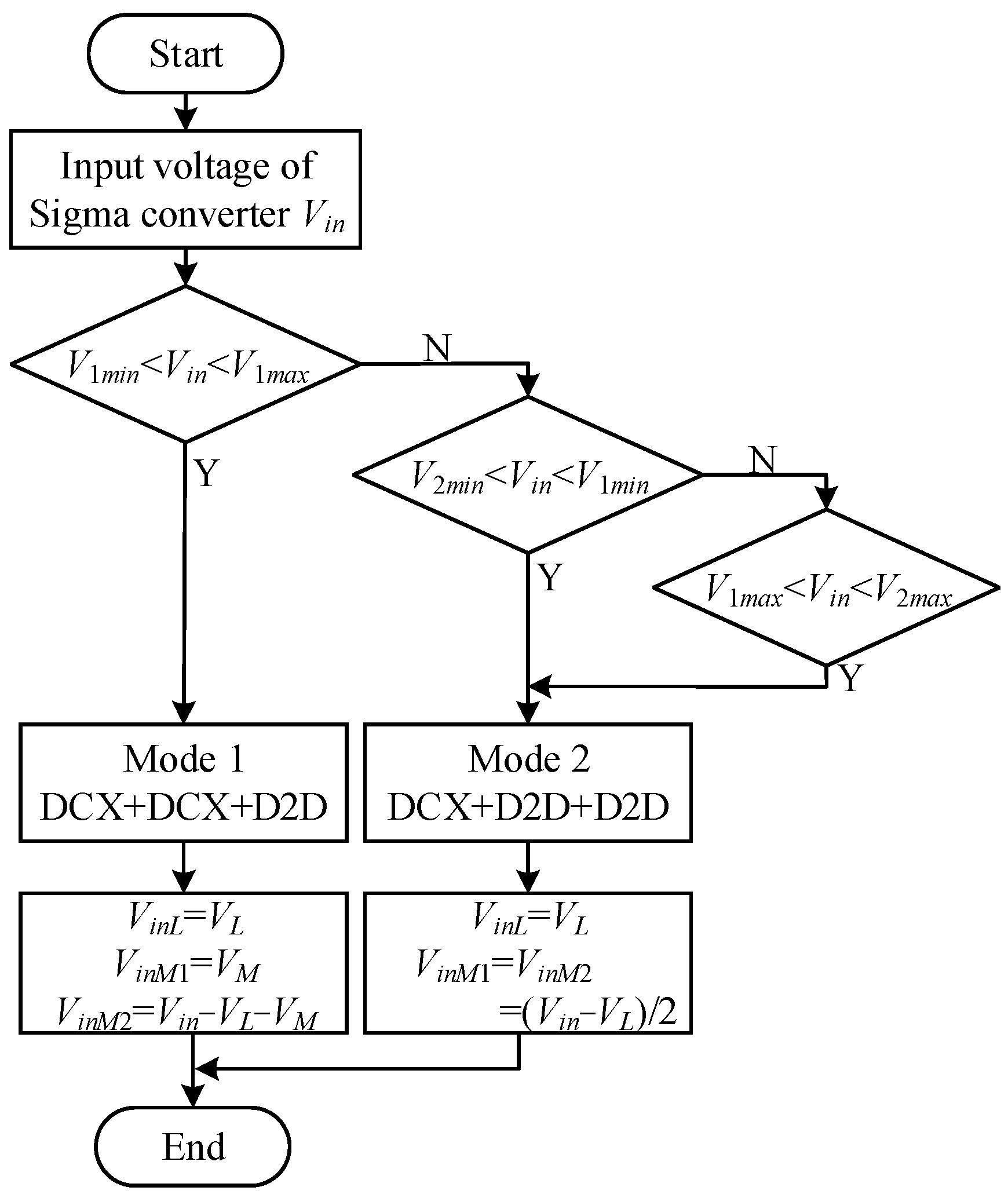
3. Operating Principle of Sigma Converter

As mentioned above, the LLC converter works in the DCX mode to enhance overall efficiency, and the multi-resonant converter can handle a wide input voltage range. However, when just one multi-resonant converter is insufficient for the input voltage range regulation, the other one should be changed to a D2D converter to provide assistance. Thus, the Sigma converter in Figure 1 can operate in two different modes in response to different input voltage ranges as follows.
(1) Mode 1 (DCX + DCX + D2D): when multi-resonant converter #2 can handle the input voltage range itself, multi-resonant converter #1 can just operate in the DCX mode to help enhance the overall efficiency.
(2) Mode 2 (DCX + D2D + D2D): when multi-resonant converter #2 cannot handle the input voltage range itself, multi-resonant converter #1 should change its operation mode from DCX to D2D.
Normally, the LLC resonant converter and its variants adopt pulse frequency modulation (PFM). Figure 5 shows a uniform controller of the Sigma converter.
Due to the two multi-resonant converters sharing the same parameters, they have the same rated input voltage VM. Assuming the input voltage range of the two multi-resonant converters is within (VM1~VM2) and the rated input voltage of the LLC–DCX converter is VL, the rated input voltage of the Sigma converter can be expressed as
V i n n o m = V L + 2 V M

3.1. Mode 1

Mode 1 (DCX + DCX + D2D): In this mode, multi-resonant converter #1 operates in the DCX mode to help enhance the overall efficiency, and multi-resonant converter #2 operates as a D2D converter to handle wide input voltage.
At this time, the input voltage of LLC–DCX and multi-resonant converter #1 maintain their own rated voltages, and multi-resonant converter #2 operates between VM1 and VM2. Thus, the minimum and maximum input voltages of the Sigma converter can be calculated as follows:
V 1 m i n = V L + V M + V M 1
V 1 m a x = V L + V M + V M 2
When the overall input voltage changes between the above ranges shown in (12) and (13), the LLC–DCX converter and multi-resonant converter #1 are open-loop control, operating at their own fixed resonant frequencies. Whereas, multi-resonant converter #2 is closed-loop control, and a proportional–integral controller is adopted to regulate the output voltage.

3.2. Mode 2

Mode 2 (DCX + D2D + D2D): When multi-resonant converter #2 cannot handle the input voltage range itself, multi-resonant converter #1 should operate as a D2D converter.
At this time, the input voltage of LLC–DCX maintains its own rated voltage, and multi-resonant converters #1 and #2 both operate between VM1 and VM2. Thus, the minimum and maximum input voltages of the Sigma converter can be calculated as
V 2 m i n = V L + 2 V M 1
V 2 m a x = V L + 2 V M 2
Similar to the control method of mode 1, when the input voltage of the Sigma converter changes between the voltage ranges in (14) and (15) in mode 2, the LLC–DCX converter adopts open-loop control. Whereas, multi-resonant converters #1 and #2 both adopt closed-loop droop control to regulate the output voltage.

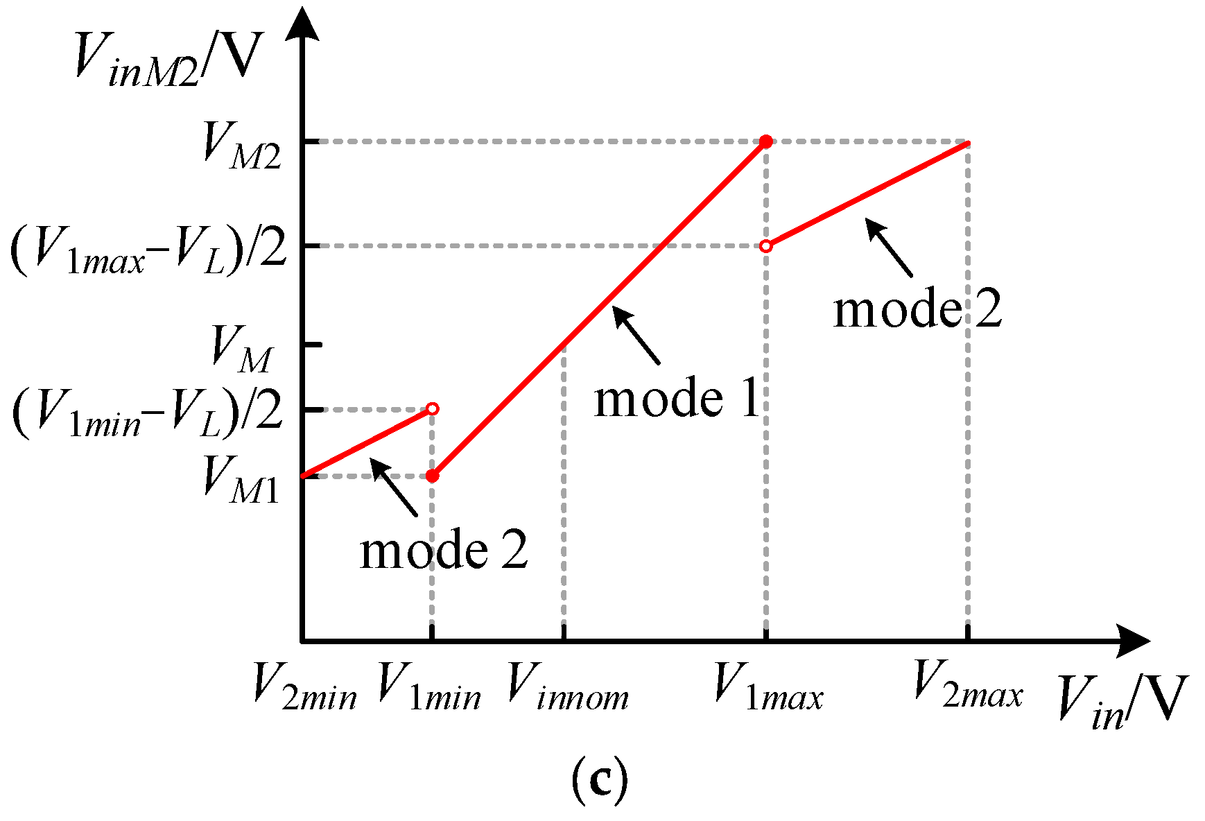
3.3. Relationship between Each Modular Input Voltage and Total Input Voltage in Different Modes

Based on the previous analysis, the relationship between the input voltages of the three submodules and the input voltage of the Sigma converter can be summarized as shown in Figure 6.
For each submodule, the input voltage is relevant to Vin, and the relationship curves are as shown in Figure 7. In this case, the LLC–DCX converter always operates at the resonant frequency, and its input voltage VinL is always constant. The input voltages VinM1 and VinM2 of multi-resonant converter #1 and multi-resonant converter #2 vary with the input voltage of the Sigma converter and operate in different modes.

4. Key Parameter Design

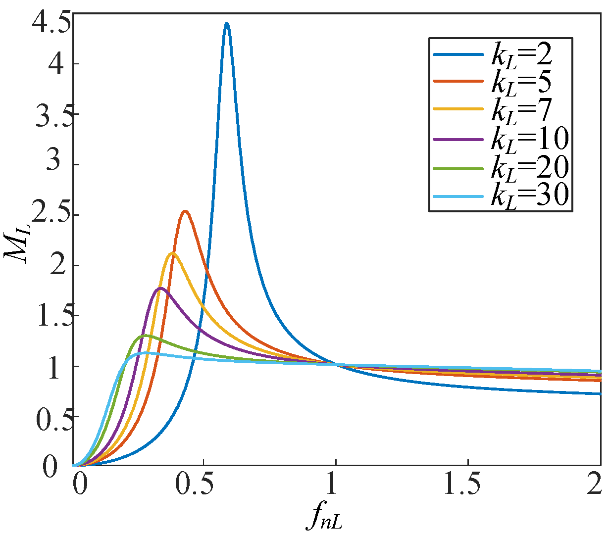
4.1. Resonant Inductance of LLC–DCX Converter

The LLC–DCX converter works at the quasi-resonant point with the best efficiency, which means that the gain maintains at 1 and has no relationship with the load. But, in reality, as the operating conditions, such as voltage, current, temperature change, and aging effects, the values of the resonant components will also change, which means that the highest efficiency will be lost.
Assuming that the tolerance of the resonant components will cause a 10% change in the resonant frequency, the worst-case scenario is the normalized switching frequency fnL being equal to 0.9 and 1.1. Then, the deviation between the actual voltage gain and the ideal gain is as shown in Table 1.
Here, kL and fnL are the inductance ratio and normalized switching frequency, respectively. They can be expressed as
k L = L m L L r L ,   f n L = f s L f r L
where fsL and frL are the switching frequency and resonant frequency, respectively, of the LLC–DCX converter.
It can be seen in Table 1 that the inductance ratio kL increases with the deviation decreases. It means that even if the value of the resonant components changes with kL, the voltage gain ML is still close to the ideal value 1. Therefore, an effective method to reduce the impact of changes in resonant components is to select a high kL during parameter design. The curves of voltage gain ML changing with kL are shown in Figure 8. It can be seen that the larger the inductance ratio kL, the flatter the curve. Due to DCX operation, the converter can choose a large inductance ratio. But, if kL is excessively large, the reduction in resonant inductance will bring an increase in the resonant capacitor, leading to a large volume and low power density. Taking all these factors into consideration, kL = 20 is selected in this paper.

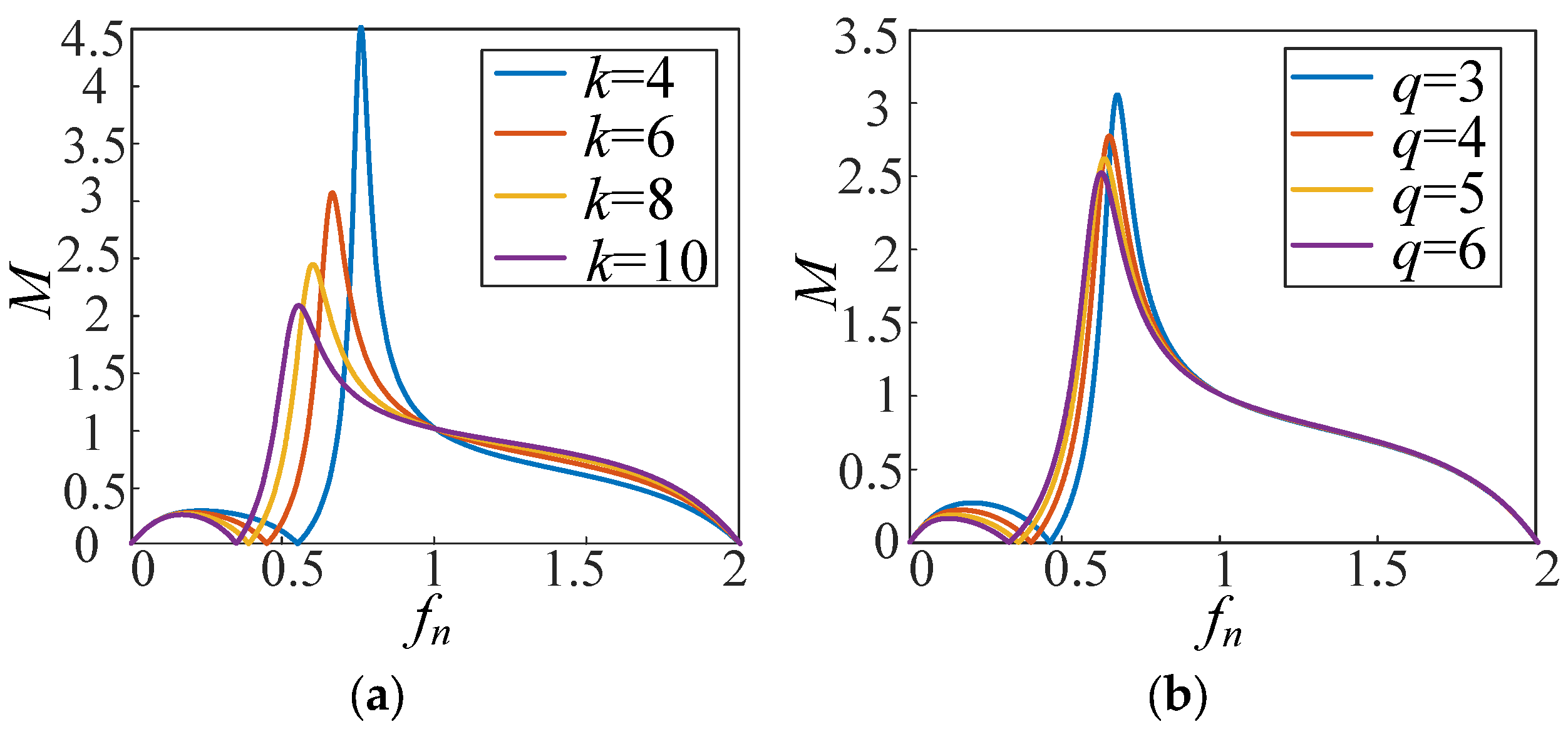
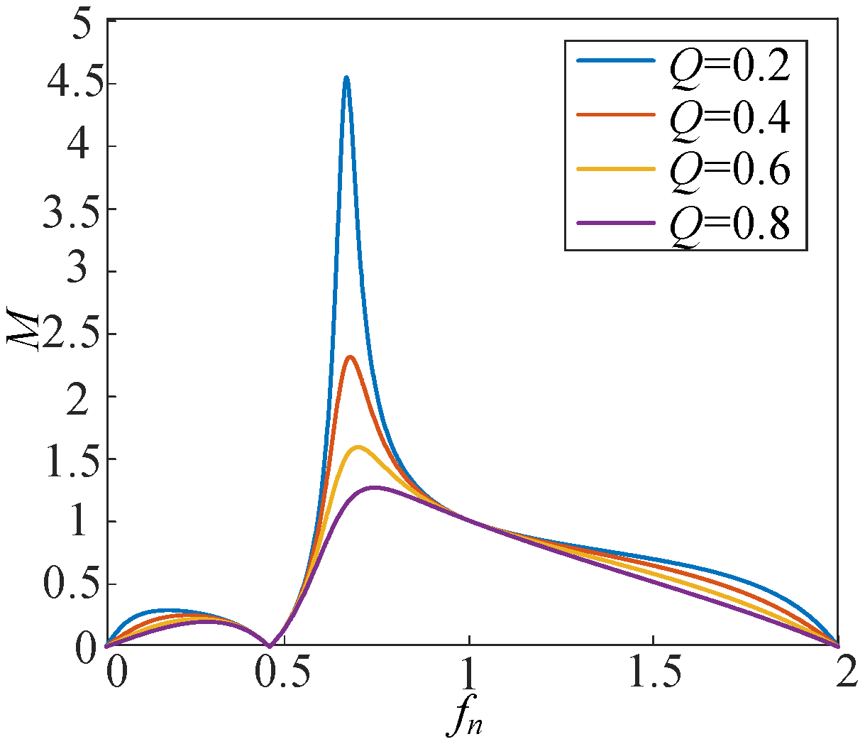
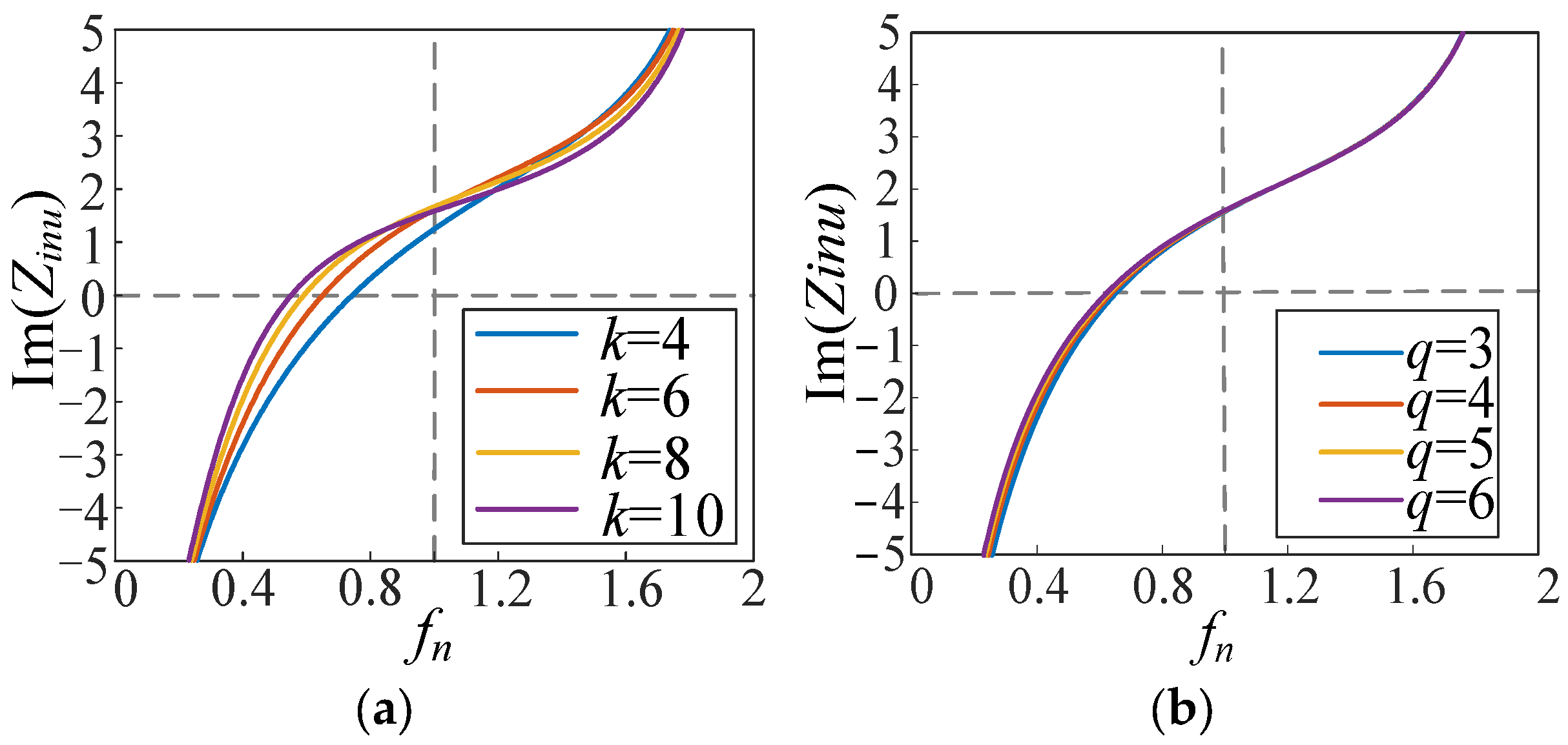
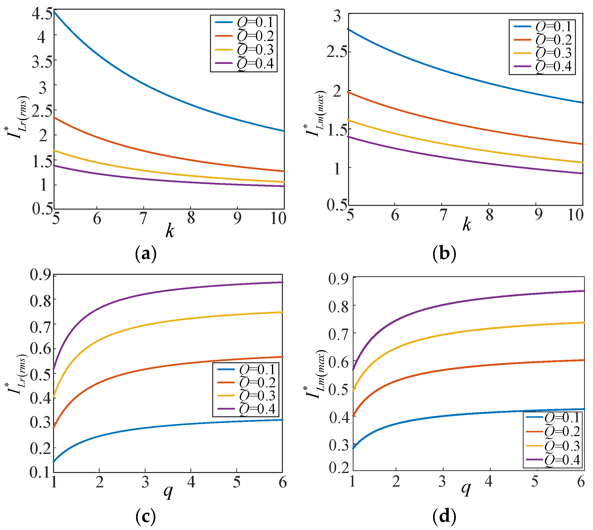
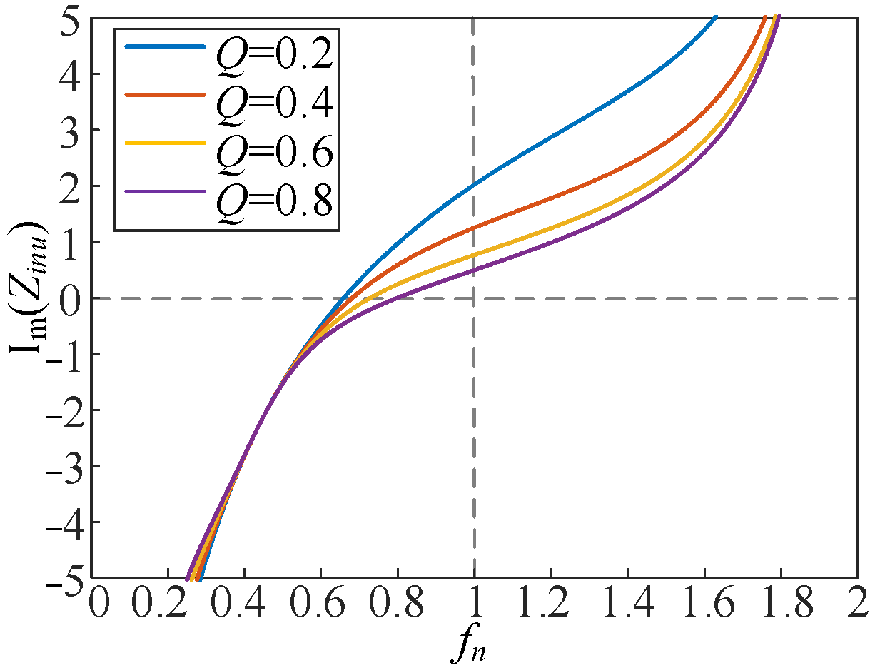
4.2. Design of k, q, and Q of Multi-Resonant Converter

Reasonable parameter design contributes to higher efficiency and power density in converters. The design of k, q, and Q of the multi-resonant converter should consider three aspects, i.e., voltage gain, input impedance, and efficiency.
The input equivalent impedance Zin of the resonant tank can be expressed as
Z i n = j ω s L r + ( j ω s L p + 1 j ω s C r ) 1 j ω s C p + R e q ( j ω s L m + 1 j ω s C m )
where ωs = 2πfs is the angular frequency. Based on (17), the imaginary part of Zin in p.u. value can be calculated as
Im ( Z i n u ) = f n η + 1 f n h η ( f n p η 1 f n η ) f n p η 1 f n h η 1 f n η + ( f n k η 1 f n q η ) 1 + Q 2 ( f n k η 1 f n q η ) 2
Apart from voltage gain M in (7)–(9) and Im(Zinu) in (18), the RMS value of the resonant current (ILr(rms)) and the peak value of the excitation current (ILm(max)) can also be affected by k, q, and Q. Meanwhile, ILr(rms) and ILm(max) have an important impact on system efficiency. The resonant current iLr(t) and excitation current iLm(t) can be expressed as
i L r ( t ) = 2 I L r ( r m s ) sin ( ω r 1 t + φ ) + 2 3 I L r ( r m s ) sin ( 3 ω r 1 t + φ )
i L m ( t ) = { n M V o L e q t n M V o 4 L e q f r 1 0 t < 1 2 f r 1 n M V o L e q t + 3 4 n M V o L e q f r 1 1 2 f r 1 t < 1 f r 1
where ωr1 is the angular frequency and ωr1 = 2πfr1; Leq is the equivalent excitation inductance of the excitation branch. Leq at the resonant point can be expressed as
L e q = L m 1 ω r 1 2 C m
Based on (19)~(21), ILr(rms) and ILm(max) can be calculated as follows:
{ I L r ( r m s ) = 10 n V o 4 R e q R e q 2 32 L e q 2 f r 1 2 + 288 25 π 2 I L m ( m a x ) = n V o 4 L e q f r 1
The normalized value of ILr(rms) and ILm(max) with the reference value IN = nMVo/Req can be derived as follows:
{ I L r ( r m s ) = 5 π 2 q 2 η 2 64 Q 2 ( k q η 2 1 ) 2 + 36 5 π 2 I L m ( m a x ) = π q η 2 Q ( k q η 2 1 )
(1) Design consideration of k and q
In view of the voltage gain, the curves of M varying with k and q are as shown in Figure 9. It can be seen that the curves almost overlap in the over-resonance area, which means k and q have little effect on M. In the under-resonance area, M becomes larger when k or q is smaller. Thus, k and q should be small so that the multi-resonant converter can meet the voltage gain requirement.
From the perspective of the input impedance, the curves of Im(Zinu) are as shown in Figure 10. It can be seen that the inductive impedance frequency range gradually decreases as k or q decreases. Because one of the conditions for ZVS is inductive input impedance, k and q should be large enough for the multi-resonant converter to achieve ZVS.
In view of the loss and efficiency, the curves of I*Lr(rms) and I*Lm(max) changing with k and q are as shown in Figure 11. On one hand, the larger the value of k, the higher the values of I*Lr(rms) and I*Lm(max). On the other hand, the lower the value of q, the higher the values of I*Lr(rms) and I*Lm(max). Thus, k should be large, and q should be small so that the system loss can be reduced and the efficiency can be improved.
(2) Design consideration of Q
In view of the voltage gain, the relationship between M and Q is as shown in Figure 12. It can be seen that Q decreases as the peak of M increases. Thus, Q should be small so that the voltage gain requirement can be met.
From the perspective of the input impedance, the curves of Im(Zinu) are as shown in Figure 13. As the value of Q becomes larger, the frequency range corresponding to the inductive input impedance gradually shrinks, making it harder to realize ZVS. Hence, Q should be small for ZVS.

5. Experimental Results

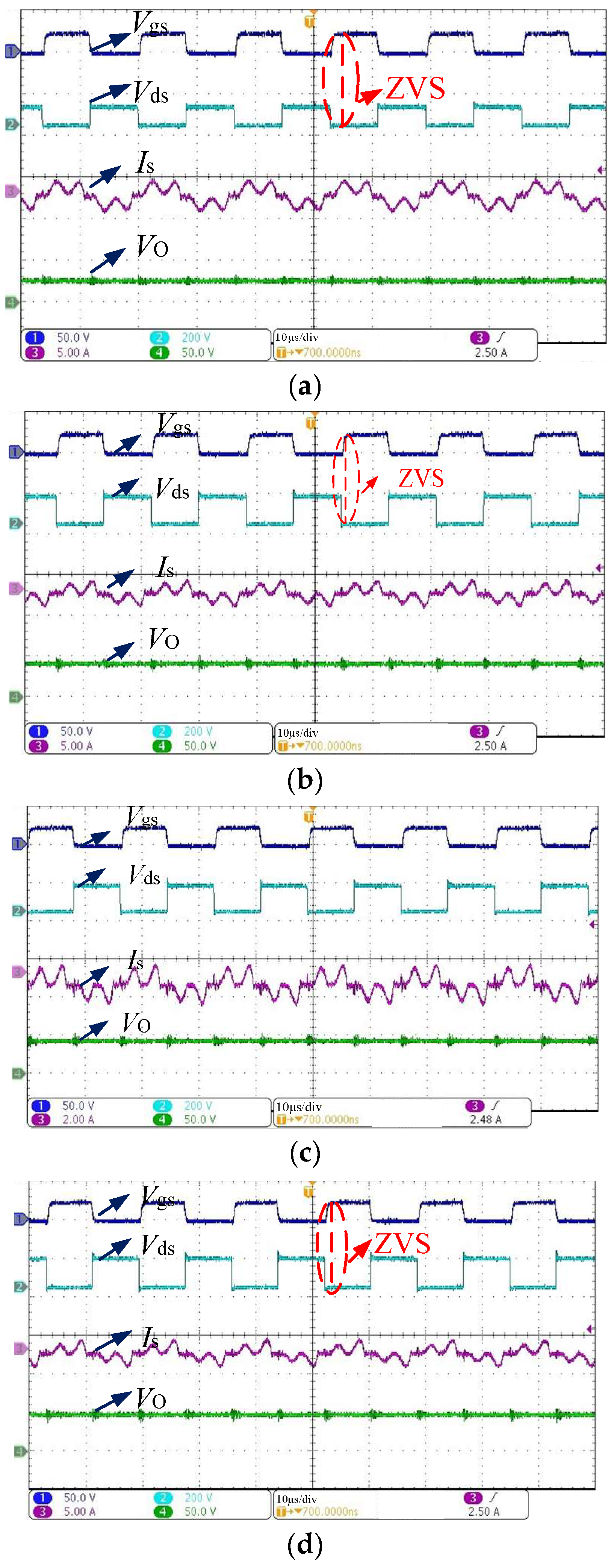
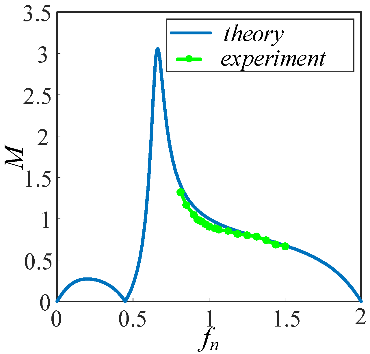
5.1. Experimental Results of Multi-Resonant Converter

The basic structure and some parameter design considerations of the multi-resonant converter are described in Section 2.2 and Section 4.2, respectively. In order to verify the accuracy of the theoretical analysis and the proposed design methodology, two sets of parameters, k = 7, q = 5.5, Q = 0.5 and k = 6, q = 3, Q = 0.3, are selected for the experiments on the multi-resonant converter. The specifications of the converter and the main parameters are shown in Table 2. The effectiveness of the parameter design can be verified by the characteristics of the voltage gain and soft switching of the multi-resonant converter, which are shown in Figure 14.
Figure 14 shows the steady-state experimental waveforms of the multi-resonant converter under different parameter conditions. In Figure 14, Vgs is the gate drive signal of Q1, Vds is the drain–source voltage of Q1, Is is the secondary side current, and Vo is the output voltage. From Figure 14, it can be seen that Vds is reduced to 0 before Vgs is turned on, indicating that the power switching tube is capable of realizing ZVS. By comparing Figure 14a with Figure 14d, it can be seen that with the quality factor Q and the resonant capacitance ratio, q, remains unchanged; when the input voltage is constant, the output voltage Vo decreases significantly with the increase in k, i.e., the voltage gain M decreases. Similarly, comparing Figure 14b with Figure 14d, it can be concluded that with the resonant inductance ratio k and resonant capacitance ratio q kept constant, when the input voltage is constant, the output voltage Vo also decreases with the increase in Q, i.e., the voltage gain becomes smaller. Similarly, comparing Figure 14c and Figure 14d, it can be seen that the output voltage Vo decreases slightly with the increase in q when the resonant inductance ratio k, the quality factor Q, and the input voltage are kept constant, and the effect of q on the voltage gain is relatively small. Based on the above comparative analysis, the experimental results are consistent with the theoretical analysis in Section 4.2.
Furthermore, in order to observe how the trend of the voltage gain M changes with the frequency fn increases, a set of experiments have been performed accordingly. The voltage gain M within the normal operation frequencies fn for k = 6, q = 3 is shown in Table 3. It can be seen that the voltage gain M changes with the increase in frequency fn. We combine the experimental results at different frequencies to make a comparison with the theoretical analysis. The specific comparison results are shown in Figure 15.
It can be seen from Figure 15 that the experimental results are basically consistent with the theoretical analysis, which shows that the theory given in Section 4.2 can provide a good prediction of the practical design of the proposed converter.

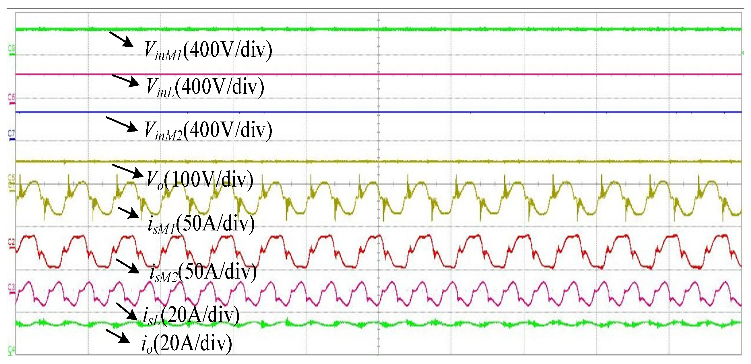
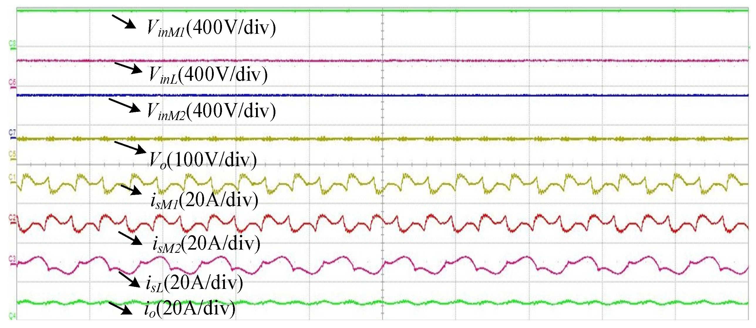
5.2. Experimental Results of Sigma Converter

A 2 kW experimental prototype of the proposed Sigma converter is built with 540~1100 V input and 48 V output voltages, as shown in Figure 16. The detailed specifications are listed in Table 4. TMS320F28377D is chosen as the digital signal processor (DSP) for system control.
Figure 17 shows the steady-state experimental waveforms of the proposed Sigma converter when the input voltage is 540 V. From the previous theoretical analysis, it can be concluded that when the input voltage is between 540 V and 645 V, multi-resonant converter #1 operates in the D2D mode, i.e., the Sigma converter operates in mode 2. At this point, the input voltage of the two multi-resonant converters is 1/2 × (VinVinL). As can be seen in Figure 17, the input voltage of the LLC–DCX converter is 270 V, and each of the two multi-resonant converters is approximately 135 V, which is consistent with the theoretical analysis.
Figure 18 shows the steady-state experimental waveforms when the input voltage is 750 V. When the input voltage is between 645 V and 925 V, multi-resonant converter #1 operates in the DCX mode, i.e., the Sigma converter operates in mode 1. As can be seen in Figure 18, the input voltage of the LLC–DCX converter is 270 V, and the input voltage of multi-resonant converter #1 is approximately 235 V; thus multi-resonant converter #2 is approximately 245 V, which is consistent with the theoretical analysis.
Figure 19 shows the steady-state experimental waveforms when the input voltage is 1100 V. When the input voltage is between 925 and 1100 V, multi-resonant converter #1 operates in the D2D mode, i.e., the Sigma converter operates in mode 2. At this point, the input voltage of the two multi-resonant converters is 1/2 × (VinVinL). As can be seen in Figure 19, the input voltage of the LLC–DCX converter is 270 V, and that of the two multi-resonant converters is approximately 415 V, which is consistent with the theoretical analysis.

6. Conclusions

In order to achieve flexible voltage regulation over a high and wide input voltage range, a modular Sigma DC/DC converter composed of an LLC–DCX converter and multi-resonant converter is proposed in this paper. Among them, the LLC–DCX converter operates at the resonant frequency to ensure high efficiency, and one of the multi-resonant converters works as a D2D converter to regulate the voltage. In addition, if the input voltage is too wide, another converter operates as a D2D converter; otherwise, it operates in the DCX mode to enhance the overall efficiency. The key considerations of each submodular and system operation modes are analyzed in detail. Finally, an experimental prototype is built, and the experimental results show that the proposed Sigma converter can maintain a constant output voltage over a wide input voltage range of 540 V to 1100 V. Moreover, the proposed topology and control method can also be extended to more modular and higher-voltage applications.

Author Contributions

Conceptualization, C.R. and X.H. (Xiaoqing Han); methodology, C.R. and X.H. (Xiangning He); validation, X.L.; data curation, Y.Q.; writing—original draft preparation, Y.H. (Yue Hui); writing—review and editing, Y.H. (Yapeng He) and C.R.; supervision, X.H. (Xiangning He). All authors have read and agreed to the published version of the manuscript.

Funding

This research was funded by the Key R&D Plan of Shanxi Province (grant number: 202102060301012) and the National Natural Science Foundation of China (grant number: 51807130).

Data Availability Statement

The data that support the findings of this study are available from the corresponding author via [email protected].

Conflicts of Interest

The authors declare no conflicts of interest.

References

  1. Grazian, F.; Soeiro, T.B.; Bauer, P. Voltage/Current Doubler Converter for an Efficient Wireless Charging of Electric Vehicles With 400-V and 800-V Battery Voltages. IEEE Trans. Ind. Electron. 2023, 70, 7891–7903. [Google Scholar] [CrossRef]
  2. Kim, J.; Ryu, S.W.; Kim, M.; Jung, J.W. Triple-Mode Isolated Resonant Buck–Boost Converter Over Wide Input Voltage Range for Residential Applications. IEEE Trans. Ind. Electron. 2021, 68, 11087–11099. [Google Scholar] [CrossRef]
  3. Wang, W.; Liu, Y.; Zhao, J.; Zhang, P.; Loh, P.C. A Dynamic Control Method for Buck + LLC Cascaded Converter with a Wide Input Voltage Range. IEEE Trans. Power Electron. 2023, 38, 1522–1534. [Google Scholar] [CrossRef]
  4. Heydari-doostabad, H.; O’Donnell, T. A Wide-Range High-Voltage-Gain Bidirectional DC–DC Converter for V2G and G2V Hybrid EV Charger. IEEE Trans. Ind. Electron. 2022, 69, 4718–4729. [Google Scholar] [CrossRef]
  5. Li, W.; Luo, Q.; Mei, Y.; Zong, S.; He, X.; Xia, C. Flying-Capacitor-Based Hybrid LLC Converters with Input Voltage Autobalance Ability for High Voltage Applications. IEEE Trans. Power Electron. 2016, 31, 1908–1920. [Google Scholar] [CrossRef]
  6. Zhang, F.; Yang, X.; Ren, Y.; Feng, L.; Chen, W.; Pei, Y. A hybrid active gate drive for switching loss reduction and voltage balancing of series-connected IGBTs. IEEE Trans. Power Electron. 2017, 32, 7469–7481. [Google Scholar] [CrossRef]
  7. Hou, N.; Gunawardena, P.; Wu, X.; Ding, L.; Zhang, Y.; Li, Y. An input-oriented power sharing control scheme with fast-dynamic response for ISOP DAB dc-dc converter. IEEE Trans. Power Electron. 2021, 37, 6501–6510. [Google Scholar] [CrossRef]
  8. Wang, Y.; Guan, Y.; Fosso, O.B.; Molinas, M.; Chen, S.Z.; Zhang, Y. An Input-Voltage-Sharing Control Strategy of Input-Series-Output-Parallel Isolated Bidirectional DC/DC Converter for DC Distribution Network. IEEE Trans. Power Electron. 2022, 37, 1592–1604. [Google Scholar] [CrossRef]
  9. Liu, F.; Zhou, G.; Ruan, X.; Ji, S.; Zhao, Q.; Zhang, X. An Input-Series-Output-Parallel Converter System Exhibiting Natural Input-Voltage Sharing and Output-Current Sharing. IEEE Trans. Ind. Electron. 2021, 68, 1166–1177. [Google Scholar] [CrossRef]
  10. Liu, Y.; Wu, H.; Ge, Z.; Ji, G. Magnetic Integration for Multiple Resonant Converters. IEEE Trans. Ind. Electron. 2023, 70, 7604–7614. [Google Scholar] [CrossRef]
  11. Sun, J.; Xu, M.; Reusch, D.; Lee, F.C. High efficiency quasi-parallel voltage regulators. In Proceedings of the 2008 Twenty-Third Annual IEEE Applied Power Electronics Conference and Exposition, Austin, TX, USA, 24–28 February 2008. [Google Scholar]
  12. Yao, J.; Chen, W.; Xue, C.; Yuan, Y.; Wang, T. An ISOP Hybrid DC Transformer Combining Multiple SRCs and DAB Converters to Interconnect MVDC and LVDC Distribution Networks. IEEE Trans. Power Electron. 2020, 35, 11442–11452. [Google Scholar] [CrossRef]
  13. Liao, Y.; Xu, G.; Sun, Y.; Peng, T.; Su, M.; Guo, B.; Xiong, W. Single-Stage DAB-LLC Hybrid Bidirectional Converter with Tight Voltage Regulation Under DCX Operation. IEEE Trans. Ind. Electron. 2021, 68, 293–303. [Google Scholar] [CrossRef]
  14. Liao, Y.; Xu, G.; Peng, T.; Sun, Y.; Liu, D.; Yang, Y.; Su, M. An LLC-DAB Bidirectional DCX Converter with Wide Load Range ZVS and Reduced Switch Count. IEEE Trans. Power Electron. 2022, 37, 2250–2263. [Google Scholar] [CrossRef]
  15. Mustafa, A.; Mekhilef, S. Dual phase LLC resonant converter with variable frequency zero circulating current phase-shift modulation for wide input voltage range applications. IEEE Trans. Power Electron. 2021, 36, 2793–2807. [Google Scholar] [CrossRef]
  16. Awasthi, A.; Bagawade, S.; Jain, P.K. Analysis of a Hybrid Variable-Frequency-Duty-Cycle-Modulated Low-Q LLC Resonant Converter for Improving the Light-Load Efficiency for a Wide Input Voltage Range. IEEE Trans. Power Electron. 2021, 36, 8476–8493. [Google Scholar] [CrossRef]
  17. Jovanović, M.M.; Irving, B.T. On-the-Fly Topology-Morphing Control—Efficiency Optimization Method for LLC Resonant Converters Operating in Wide Input- and/or Output-Voltage Range. IEEE Trans. Power Electron. 2016, 31, 2596–2608. [Google Scholar] [CrossRef]
  18. Sun, X.; Li, X.; Shen, Y.; Wang, B.; Guo, X. Dual-Bridge LLC Resonant Converter with Fixed-Frequency PWM Control for Wide Input Applications. IEEE Trans. Power Electron. 2017, 32, 69–80. [Google Scholar] [CrossRef]
  19. Wu, X.; Li, R.; Cai, X. Modified LLC Resonant Converter with LC Antiresonant Circuit in Parallel Branch for Wide Voltage Range Application. IEEE Trans. Power Electron. 2022, 37, 7387–7399. [Google Scholar] [CrossRef]
  20. Sun, W.; Xing, Y.; Wu, H.; Ding, J. Modified high-efficiency LLC converters with two split resonant branches for wide input-voltage range applications. IEEE Trans. Power Electron. 2018, 33, 7867–7879. [Google Scholar] [CrossRef]
  21. Zhang, X.; Jing, J.; Guan, Y.; Dai, M.; Wang, Y.; Xu, D. High-Efficiency High-Order CL-LLC DC/DC Converter with Wide Input Voltage Range. IEEE Trans. Power Electron. 2021, 36, 10383–10394. [Google Scholar] [CrossRef]
  22. Zhao, Q.; Liu, W.; Wang, Y.; Wang, D.; Wu, N. A Novel Multiresonant DC–DC Converter with Wide Output-Voltage Range. IEEE Trans. Power Electron. 2020, 35, 5625–5638. [Google Scholar] [CrossRef]
  23. Wu, H.; Jin, X.; Hu, H.; Xing, Y. Multielement Resonant Converters with a Notch Filter on Secondary Side. IEEE Trans. Power Electron. 2016, 31, 3999–4004. [Google Scholar] [CrossRef]
  24. Jung, J.-H.; Kim, H.-S.; Ryu, M.-H.; Baek, J.-W. Design Methodology of Bidirectional CLLC Resonant Converter for High-Frequency Isolation of DC Distribution Systems. IEEE Trans. Power Electron. 2013, 28, 1741–1755. [Google Scholar] [CrossRef]
Figure 1. Structure of Sigma converter.
Electronics 13 00995 g001
Figure 2. Structure of proposed Sigma DC/DC converter. (a) Overall system structure; (b) LLC–DCX converter; (c) multi-resonant converter.
Electronics 13 00995 g002
Figure 3. Simplified model of multi-resonant converter.
Electronics 13 00995 g003
Figure 4. Gain curves of multi-resonant converter.
Electronics 13 00995 g004
Figure 5. Controller of proposed converter.
Electronics 13 00995 g005
Figure 6. Flow chart of operation modes with different input voltage ranges.
Electronics 13 00995 g006
Figure 7. Relationship between three modular input voltages and total input voltage. (a) Vi—LVin; (b) Vin—1Vin; (c) Vin—2Vin.
Electronics 13 00995 g007aElectronics 13 00995 g007b
Figure 8. Curves of voltage gain changing with kL.
Electronics 13 00995 g008
Figure 9. Curves of voltage gain changing with k and q. (a) M changing with k; (b) M changing with q.
Electronics 13 00995 g009
Figure 10. Curves of imaginary part of input impedance. (a) Im(Zinu) changing with k; (b) Im(Zinu) changing with q.
Electronics 13 00995 g010
Figure 11. Curves of I*Lr(rms) and I*Lm(max). (a) I*Lr(rms) changing with k; (b) I*Lm(max) changing with k; (c) I*Lr(rms) changing with q; (d) I*Lm(max) changing with q.
Electronics 13 00995 g011
Figure 12. Curves of voltage gain changing with Q.
Electronics 13 00995 g012
Figure 13. Curves of input impedance changing with Q.
Electronics 13 00995 g013
Figure 14. Experimental waveforms of multi-resonant converter. (a) Experimental waveforms with k = 7, q = 3, Q = 0.3; (b) experimental waveforms with k = 6, q = 3, Q = 0.5; (c) experimental waveforms with k = 6, q = 5.5, Q = 0.3; (d) experimental waveforms with k = 6, q = 3, Q = 0.3.
Electronics 13 00995 g014
Figure 15. Comparison between theoretical analysis and experimental results, with k = 6, q = 3.
Electronics 13 00995 g015
Figure 16. Experimental prototype of Sigma converter.
Electronics 13 00995 g016
Figure 17. Experimental waveforms with Vin = 540 V.
Electronics 13 00995 g017
Figure 18. Experimental waveforms with Vin = 750 V.
Electronics 13 00995 g018
Figure 19. Experimental waveforms with Vin = 1100 V.
Electronics 13 00995 g019
Table 1. Deviation of voltage gain.
kLfnL = 0.9Error1fnL = 1.1Error2
kL = 21.1320.1320.91960.0804
kL = 51.0480.0480.96640.0336
kL = 71.0330.0330.97510.0249
kL = 101.0230.0230.98260.0174
kL = 201.0110.0110.99090.0091
kL = 301.0070.0070.99350.0065
Table 2. Specifications of multi-resonant converter.
SymbolParameterValue (k = 6, q = 3, Q = 0.3)Value (k = 7, q = 5.5, Q = 0.5)
VinInput voltage135–415 V135–415 V
VoOutput voltage48 V48 V
PoOutput power500 W500 W
nMTurn ratio6:16:1
fr1Resonant frequency80 kHz80 kHz
LrResonant inductance29.4 μH43 μH
LpResonant inductance70.6 μH103.2 μH
LmMagnetizing inductance176.4 μH301 μH
CrResonant capacitor37.4 nF26 nF
CpResonant capacitor22.4 nF15.6 nF
CmCapacitor112.2 nF143 nF
Table 3. Voltage gain variation with frequency for k = 6, q = 3.
ValueValueValueValueValueValueValueValue
fn0.820.850.90.9250.950.97511.038
M1.321.161.040.980.960.930.910.88
fn1.06251.1251.18751.251.31.371.451.5
M0.8680.850.810.80.780.740.680.67
Table 4. Specifications of prototype.
SymbolParameterValue
VinInput voltage540~1100 V
VoOutput voltage48 V
PoOutput power1500 W
nMTurns ratio26:5
nLTurns ratio22:4
fr1Resonant frequency80 kHz
frLResonant frequency150 kHz
LrLResonant inductance13 μH
LmLMagnetizing inductance260 μH
CrLResonant capacitor89.8 nF
LrResonant inductance29.4 μH
LpResonant inductance70.6 μH
LmMagnetizing inductance176.4 μH
CrResonant capacitor37.4 nF
CpResonant capacitor22.4 nF
CmCapacitor112.2 nF
Disclaimer/Publisher’s Note: The statements, opinions and data contained in all publications are solely those of the individual author(s) and contributor(s) and not of MDPI and/or the editor(s). MDPI and/or the editor(s) disclaim responsibility for any injury to people or property resulting from any ideas, methods, instructions or products referred to in the content.

