1. Introduction
Silicon carbide (SiC) power semiconductors have excellent characteristics such as a high breakdown field, high thermal conductivity, low on-resistance, and fast switching speed compared to those of silicon (Si) power semiconductors [
1,
2,
3,
4,
5,
6,
7]. Owing to these advantages, SiC power semiconductors are employed in various applications, such as in electric vehicle chargers [
8,
9,
10], multilevel inverters [
11], induction heaters [
12], fuel cell systems [
13], and wireless power transmission [
14].
The recent developments in power electronics technology have significantly increased the demand for higher-power-level switching devices. Despite the gradual increase in the capacity of switching devices, it remains insufficient to meet the burgeoning market demand. Against this backdrop, there has been a marked surge in interest towards the technology of parallel connection for switching devices. When operated in parallel, mismatches in typical characteristics such as threshold voltage and on-resistance, coupled with an asymmetric structure, lead to significant current imbalances, presenting a critical issue [
15,
16,
17].
In particular, SiC power semiconductors exhibit a heightened vulnerability to current imbalances when connected in parallel. The switching characteristics of SiC power semiconductors, characterized by their small input and output capacitances, are substantially influenced by the parasitic inductance present in the circuit. The existence of a discrepancy in the magnitude of parasitic inductance, due to an asymmetric structure among parallel-connected SiC devices, results in a pronounced current imbalance between the devices. This phenomenon not only escalates switching losses but also diminishes the efficiency of the power converter. Consequently, a plethora of studies has been undertaken to minimize the current imbalance between parallel-connected switching devices [
18,
19,
20,
21,
22,
23,
24,
25,
26,
27].
The severity of these issues underscores the urgent need for research aimed at resolving the problems of current imbalance among parallel-connected switching devices. Efforts to enhance the efficiency and reliability of parallel connection technologies have become an indispensable part of designing high-performance power systems.
Lu [
18] improved the current-balancing of parallel-switching devices by connecting a toroidal core to the output of a half-bridge module and adjusting the mutual inductance between the devices. However, this method requires an additional current-balancing circuit, which significantly increases volume. A current-balancing method using a common-mode choke between parallel devices was proposed in [
19,
20]. However, this method increased the parasitic inductance of the gate loop, which induced oscillations in each device. An active gate driver (AGD) that adjusts the driving voltage to improve the transient characteristics of the switching device was proposed in [
21,
22]. The AGD minimizes the current imbalance between parallel devices by adjusting the slope of the drain current at the transients. However, AGD sacrifices the switching speed for current-balancing, which diminishes the advantages of SiC power semiconductors. As reported in [
18,
19,
20,
21,
22,
23], active current-balancing methods that add a magnetic material or adjust the slope of the drain current increase the cost, volume, and complexity.
In contrast, structural current-balancing methods do not have the aforementioned disadvantages because the current imbalance is minimized through a symmetrical arrangement between switching devices connected in parallel [
24,
25,
26,
27].
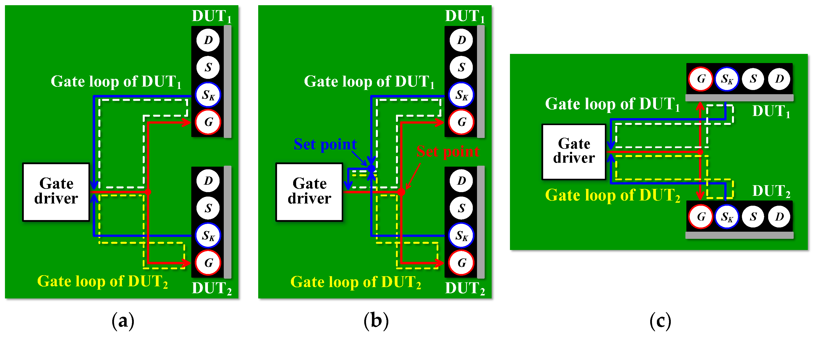
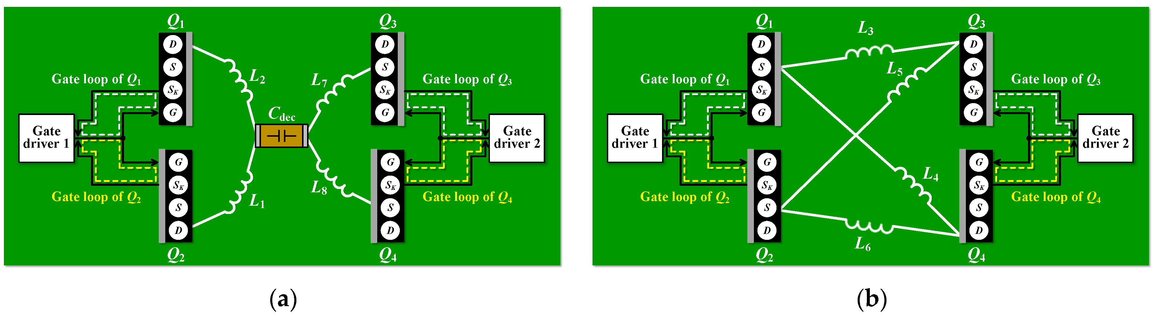
Figure 1 shows the gate loop formed by the two devices under test (DUTs) and gate drivers using the previously studied methods; the package-type of the switching device is a TO-247-4 with a Kelvin source. In
Figure 1,
D,
S,
SK, and
G represent the drain, power source, Kelvin source, and gate of the device, respectively. In [
24,
25], the current from the gate driver to the gate of each device was matched by arranging the two devices perpendicular to the gate driver output, as shown in
Figure 1a. However, there was a large difference in the length of the gate loop because the return path to the gate driver was asymmetric. Prakash et al. [
26] set a point that must be passed through to form a symmetrical gate loop, as shown in
Figure 1b. The gate loop lengths of the two devices become symmetrical when the gate loop is formed by passing through the set point. However, this method lengthens the gate loop because it must pass through the set point to satisfy symmetry. Both the symmetry and loop length must be considered because the switching characteristics of SiC power semiconductors are sensitive to parasitic inductance. Zhao et al. [
27] achieved a symmetrical gate loop by rotating the devices in
Figure 1a by 90° to the right, as shown in
Figure 1c. However, it is difficult to attach a heatsink because the lead frames of the two devices vertically face the same direction. Even if the devices are bent toward the printed circuit board (PCB) to facilitate a heatsink attachment, there must be sufficient space between DUT
1 and DUT
2, which can result in a long gate loop.
In previous studies, several methods achieved the symmetry of the gate loop. However, the symmetry of the power loop affects the current imbalance. The symmetry of the power loop inductance should be considered in detail when constructing a half-bridge with parallel-connected devices. However, most published papers reported only achieving gate loop symmetry without considering the power loop.
In this study, a half-bridge switching power module (HBSPM) based on parallel-connected SiC MOSFETs with a symmetric structure and low inductance was proposed. The effect of parasitic inductance and symmetry on parallel-connected SiC MOSFETs is analyzed, and a structure with a gate loop and power loop symmetry with low inductance is presented. The proposed HBSPM improves current imbalance through current loop symmetry and allows for easy attachment of a heatsink for practical applications. A detailed PCB layout design was also provided. The symmetry of the proposed HBSPM was analyzed in detail using ANSYS Q3D. Finally, experimental results are presented to verify the current-balancing performance of the proposed paralleled SiC MOSFETs based HBSPM.
The rest of the article is summarized as follows:
Section 2 introduces the proposed structural current-balancing method; in
Section 3, a detail design of the HBSPM based on the proposed structural method is presented; the experimental verifications are provided in
Section 4; and
Section 5 concludes this article.
2. Proposed Half-Bridge Switching Power Module Based on Parallel-Connected SiC MOSFETs
This chapter discusses the design and implementation of a half-bridge switching power module utilizing parallel-connected SiC MOSFETs. The verification process conducted with the LTspice simulation tool is described.
Section 2.1 introduces the basic structure and operating principles of the switching power module. Following,
Section 2.2 explains the impact of gate loop inductance on switching performance and the proposed parallel connection structure to minimize it.
Section 2.3 covers the design method of the proposed half-bridge structure to overcome the effects of power loop inductance. Lastly,
Section 2.4 discusses the practical structure including a heatsink for actual applications.
2.1. Switching Power Module
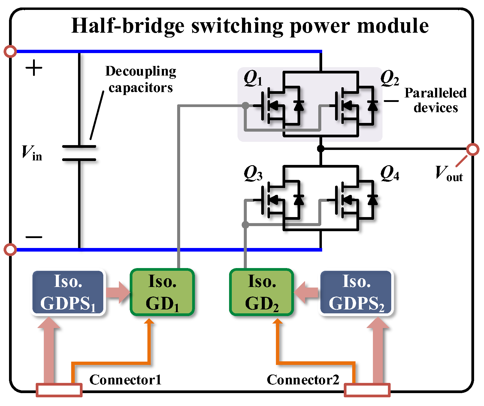
Figure 2 shows the overall structure of the proposed half-bridge switching power module based on parallel-connected SiC MOFSETs. The power stage of the proposed HBSPM includes decoupling capacitors high-side and low-side parallel-connected SiC MOSFETs
Q1–
Q4. To provide a short loop for high-frequency current during switching transients, the decoupling capacitors are placed close to the half-bridge leg. As a result, the proposed HBSPM can achieve a small power loop inductance, regardless of the structure of the main board connected to the module. The output of the HBSPM
Vout represents the pole voltage of the half-bridge leg. The signal stage comprises an isolated gate driver power supply, Iso. GDPS
1, and an isolated gate driver, Iso. GD
1, to drive high-side devices by receiving input from Connecter1, and Iso. GDPS
2 and Iso. GD
2 to drive low-side devices. A multiphase leg, such as a full-bridge or three-phase leg, can be easily implemented through parallel connections because the proposed HBSPM includes a gate driving circuit. In addition, parallel-connected SiC MOSFETs provide high efficiency in low-power applications and high-current performance in high-power applications.
2.2. Impact of Gate Loop Inductance and Proposed Parallel Connection Structure
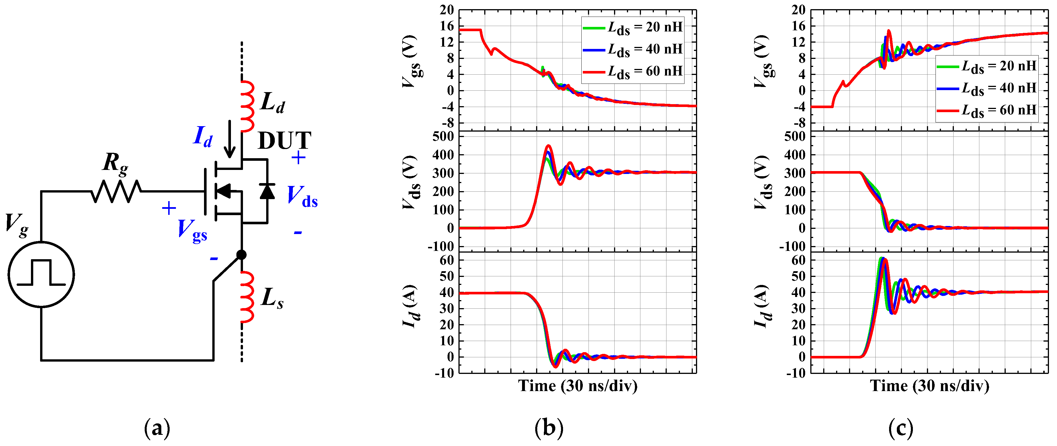
Figure 3a shows the gate loop of a single switching device with the parasitic inductance of the gate loop
Lg. In the gate loop,
Lg forms an
R-
L-
C circuit with the gate resistance
Rg and gate-source capacitance
Cgs of the DUT. As a result, the transfer function of the gate-source voltage
Vgs to the driving voltage
Vg exhibits the characteristics of a second-order system [
20]. If
Lg increases, the damping ratio of the transfer function decreases, which in turn increases the overshoot of
Vgs. Additionally, the transfer function has a natural frequency that is determined by
Lg and
Cgs. As
Lg increases, the natural frequency decreases, leading to an increase in the fall and rise time of
Vgs during switching transients [
28].
Figure 3b,c show the impact of
Lg on the switching characteristics of the DUT in
Figure 3a. The selection of
Lg values at 10 nH, 20 nH, and 30 nH was aimed at observing the trend within the realistic range of gate loop inductances encountered in typical switching circuits. This approach helps to provide a clear understanding of how different levels of inductance affect the operation of DUT during both turn-on and turn-off transients.
Figure 3b shows the
Vgs, drain-source voltage
Vds, and drain current
Id at the turn-off transient when
Lg is 10 nH, 20 nH, and 30 nH, respectively. When
Lg increases, the damping ratio of the transfer function decreases, causing an increase in the undershoot of
Vgs and resulting in instability during the turn-off transient. Moreover, due to the increased fall time of
Vgs,
Vds and
Id start changing later. As shown in
Figure 3c, an increase in
Lg results in an increase in the overshoot and rise time of
Vgs during the turn-on transient. This implies that the turn-on and off delay increase, and the waveform of
Vgs becomes unstable when the gate loop inductance increases.
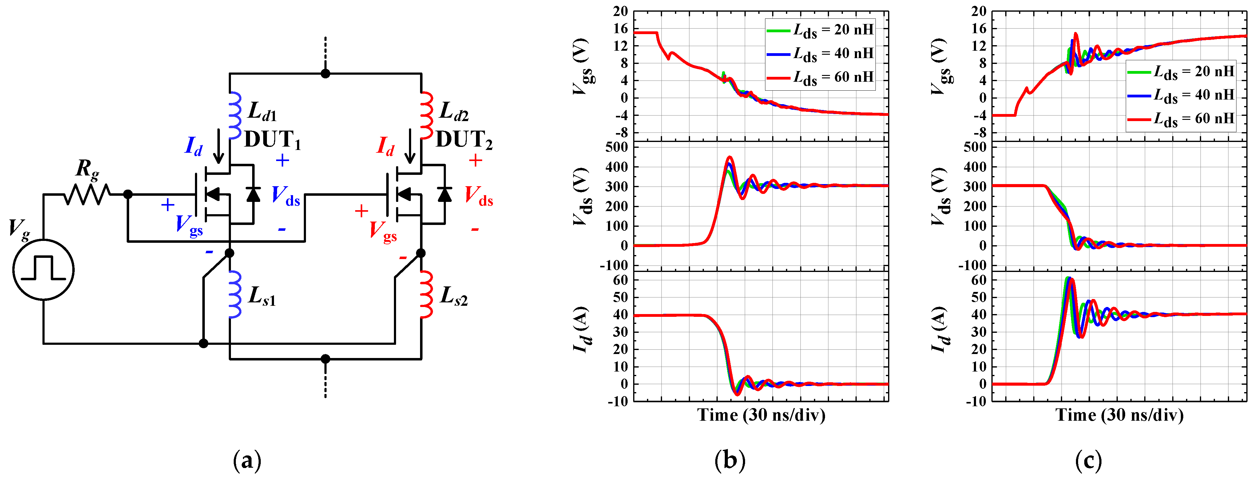
Figure 4a shows the gate loops of parallel-connected devices with gate loop inductance, and
Figure 4b,c show the impact of the gate loop inductance imbalance on the parallel-connected devices. The asymmetry of
Lg between parallel-connected devices leads to a difference in the fall and rise time, resulting in a current imbalance during switching transients.
Figure 4b shows the
Vgs,
Vds, and
Id of each device at the turn-off transient when the gate loop inductance of DUT
1 Lg1 is 10 nH and the gate loop inductance of DUT
2 Lg2 is 20 nH. The
Vgs of DUT
1 decreases faster than that of DUT
2, and the
Id of DUT
1 starts to decrease faster as well because
Lg1 is smaller than
Lg2. Therefore, the
Id of DUT
2 rises instantaneously. Even in the turn-on transient, DUT
1 begins to conduct first, which results in a large current overshoot at DUT
1, as shown in
Figure 4c. Consequently, both the magnitude of the gate loop inductance of each device and the symmetry between the devices must be considered when the devices are driven in parallel.
Figure 5 shows the proposed parallel connection structure and the gate loop of each device. As shown in
Figure 1a,b, DUT
1 and DUT
2 are positioned on the vertical line; however, DUT
2 is rotated by 180°. The gate driver is positioned horizontally from the center of the two devices.
In the proposed structure, the gate and Kelvin sources of the two devices are located at the same distance from the gate driver, and a symmetrical gate loop can be formed. In addition, when attaching the heatsink, DUT
1 is bent to the left and DUT
2 to the right so that there is no restriction on the distance between the two devices, unlike in
Figure 1c. Therefore, the proposed structure can achieve both symmetry and a short gate loop length while facilitating a heat dissipation design.
2.3. Effect of Power Loop Inductance and Proposed Half-Bridge Structure Based on Parallel-Connected SiC MOSFETs
Figure 6a shows the parasitic inductance of the power loop, comprising the drain inductance
Ld and source inductance
Ls of a single switching device. During switching transients, the induced voltage by
di/
dt across the power loop inductance increases the overshoot and ringing of
Vds. Additionally, when the power loop inductance increases, the slope of
Id decreases, which slows down the switching speed.
Figure 6b,c show the effect of the drain-source inductance
Lds, which is the sum of
Ld and
Ls, on the switching characteristics of the DUT in
Figure 6a. As shown in
Figure 6b, the oscillations of
Vds and
Id increase as
Lds increases at the turn-off transient.
Figure 6c shows the waveforms during the turn-on transient. The oscillations of the voltage and current increase with an increase in
Lds, which is similar to the turn-off transient. Moreover, an increase in
Lds leads to a decrease in the slope of
Id. If the power loop inductance of the parallel-connected devices is asymmetrical, it not only causes an increase in oscillation but also results in a current imbalance due to the difference in the slope of
Id.
Figure 7a shows the drain–source inductance of each device connected in parallel, while
Figure 7b,c show the impact of the drain–source inductance imbalance on the parallel-connected devices. The drain inductance
Ld1 and source inductance
Ls1 of DUT
1 are 10 nH and the inductances of DUT
2 (
Ld2 and
Ls2) are 20 nH. As shown in
Figure 7b,c, the gate-source and drain-source voltages of the two devices are almost the same; however, an imbalance in the drain current occurs because the
di/dt of DUT
1 with smaller
Lds is larger than that of DUT
2. More current flows to DUT
1 with a small parasitic inductance, and this increases switching loss.
The power loop inductance must be considered in more detail if a half-bridge leg is constructed using parallel-connected devices.
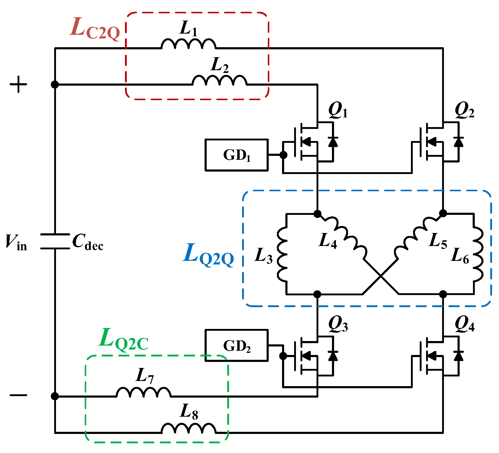
Figure 8 shows the parasitic inductance of a half-bridge leg based on parallel-connected devices.
The parasitic inductance of a half-bridge leg can be classified into three parts: the inductance LC2Q from the decoupling capacitor Cdec to the high-side devices (Q1 and Q2), inductance LQ2Q from the source of the high-side devices to drain of the low-side devices (Q3 and Q4), and inductance LQ2C from the source of the low-side devices to Cdec. For the symmetry of the power loop, the path related to the inductance of each part (e.g., L1 and L2 of LC2Q) must have the same length.
Figure 9 shows the structure of the proposed half-bridge switching power module and its parasitic inductance. In the proposed HBSPM, the high-side and low-side devices are horizontally symmetrical, and
Cdec is located at the center. As shown in
Figure 9a, the distance from the drain of
Q1 to
Cdec is the same as that from the drain of
Q2 to
Cdec; thus,
L1 and
L2 are the same. The same principle was applied to
L7 and
L8. Therefore, the inductances in
LC2Q and
LQ2C are symmetrical in the proposed structure.
Figure 9b shows the inductance in
LQ2Q. As in the previous case, the inductances (
L3–
L6 and
L4–
L5) are symmetrical because the length of each path from the source of the high-side devices to the drain of the low-side devices is the same. Therefore, the proposed half-bridge switching power module satisfies the symmetry requirements in both the gate and power loops through the parallel connection structure in
Figure 5 and the half-bridge arrangement in
Figure 9.
This structural symmetry has a positive impact on the performance of the switching power module. The symmetrical design minimizes parasitic inductance, reducing switching losses and increasing power transmission efficiency. This is particularly advantageous for high-speed switching applications, contributing to reduced power losses and increased overall system reliability. Therefore, the structure of the HBSPM proposed in this study offers an efficient and reliable solution for high-performance power electronics systems.
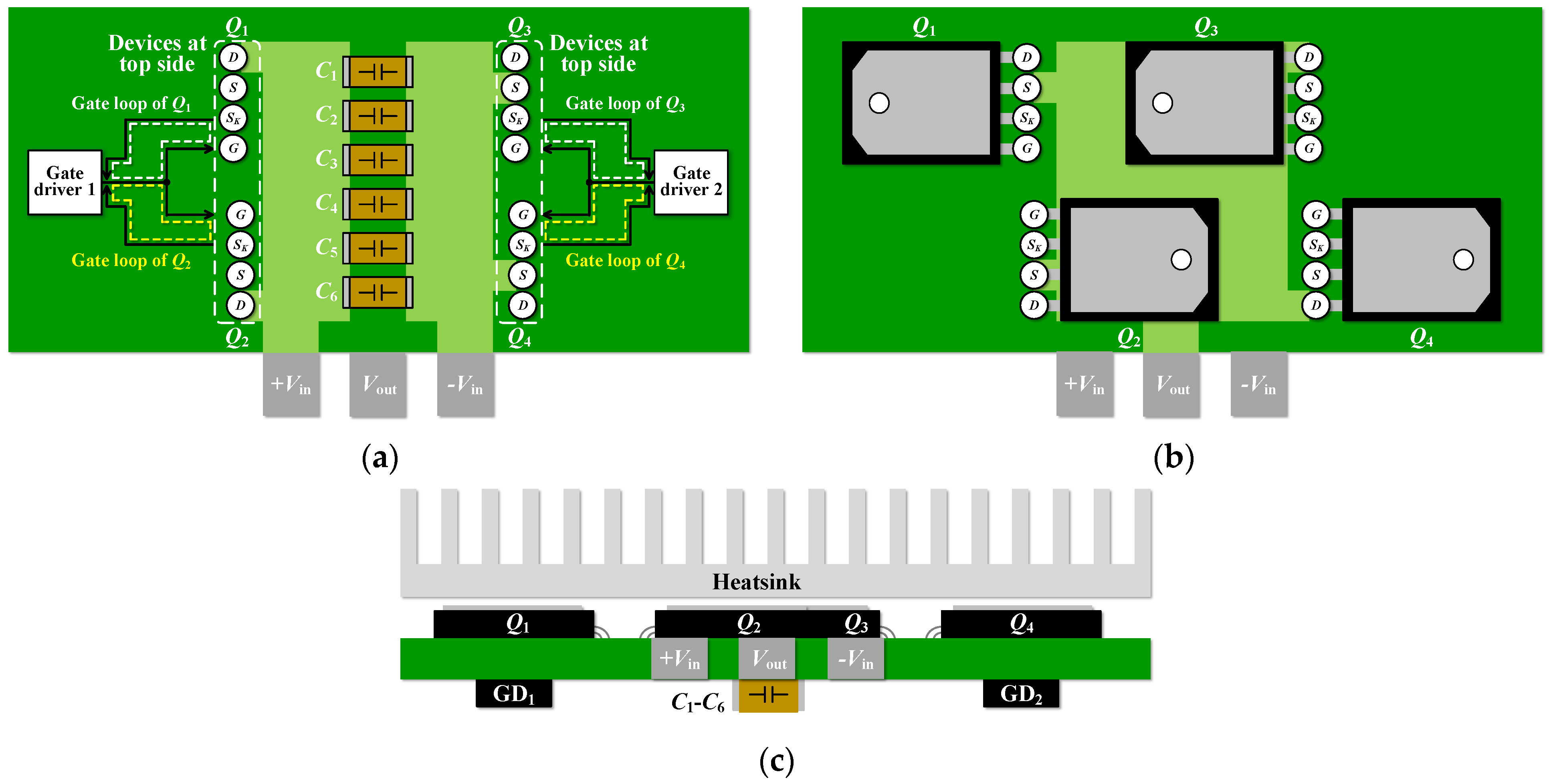
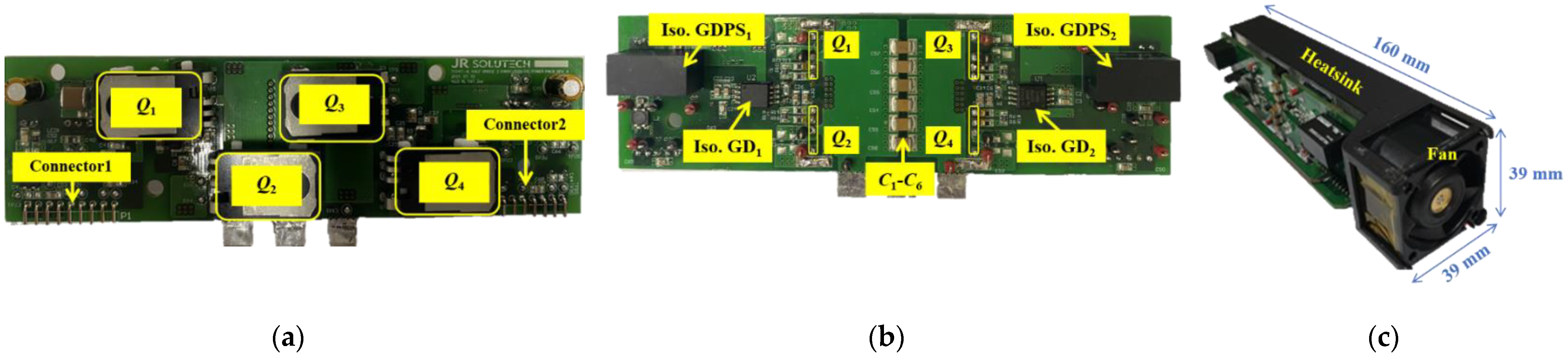
2.4. Practical Structure with Heatsink
Figure 10 shows the practical structure of the proposed switching power module. As shown in
Figure 10a, two gate drivers and six capacitors (
C1–
C6) are located at the bottom side of the HBSPM. To ensure that
Cdec can carry the current during switching transients, it must have a sufficient current rating. As a result, six capacitors are used in parallel for
Cdec. The
+Vin plane connected to the drain of the high-side devices and the
−Vin plane connected to the source of the low-side devices exist at the bottom side. As shown in
Figure 10b, the switching devices are located on the top side of the HBSPM, and there is a
Vout plan connecting the source of the high-side devices and the drain of the low-side devices, which is the output of the HBSPM. The devices on the top side were bent towards the PCB for ease of attaching the heatsink; Q
1 and Q
3 were bent to the left, and Q
2 and Q
4 were bent to the right. In this structure, the heatsink can be attached easily because the lead frames of all devices face the opposite direction of the PCB, as shown in
Figure 10c. Thus, the proposed HBSPM improves current-balancing through a symmetrical structure and can be designed as a heatsink-integrated module to achieve high efficiency and high-power density.
4. Experimental Result
The performance of the proposed half-bridge switching power module is verified under two experimental conditions. First, a double-pulse test (DPT), wherein the high-side devices were turned off and a double pulse was applied to the low-side devices, was performed to verify the current-balancing of parallel-connected SiC MOSFETs during transient switching. Considering the maximum current of 80 A for the application, the proposed HBSPM performs a double-pulse test (DPT) at 40 A for the parallel-structured low-side device. In the first pulse, the low-side devices are turned on at 0 A and turned off at 40 A. At this juncture, the off-state of the low-side devices at 40 A is analyzed. After the low-side devices stabilize, they are turned on again at 40 A during the second pulse. This procedure allows the energy stored in the load inductor to flow back into the low-side devices, during which the on-state of the low-side devices at 40 A is also analyzed.
Second, a full-bridge LLC resonant converter was designed using the proposed HBSPM, and the conduction and switching losses of parallel-connected devices were measured and compared.
Figure 16 shows the double-pulse test circuit of the proposed switching power module, and the system parameters are listed in
Table 3.
Figure 17 shows the transient waveforms of the low-side devices under a gate-source voltage of +15/−5 V, input voltage of 300 V, and a drain current of 40 A.
Vgs and
Vds of Q
3 and Q
4 are measured using a Tektronix TPP0500B passive probe (Beaverton, OR, USA), and
Id is measured using a Rogowski coil SS-284A with a 20 mV/A ratio.
As shown in
Figure 17a, the
Vgs,
Vds, and
Id of parallel-connected devices are almost the same at turn-off transient. At the turn-on transient in
Figure 17b, the
Vgs and
Vds of Q
3 and Q
4 are also almost the same; however, the drain currents are slightly different because the gate loop inductance of Q
3 is slightly larger than that of Q
4. However, the peak currents of Q
3 and Q
4 are 50 A and 51.2 A, respectively; the error is only 2.34%.
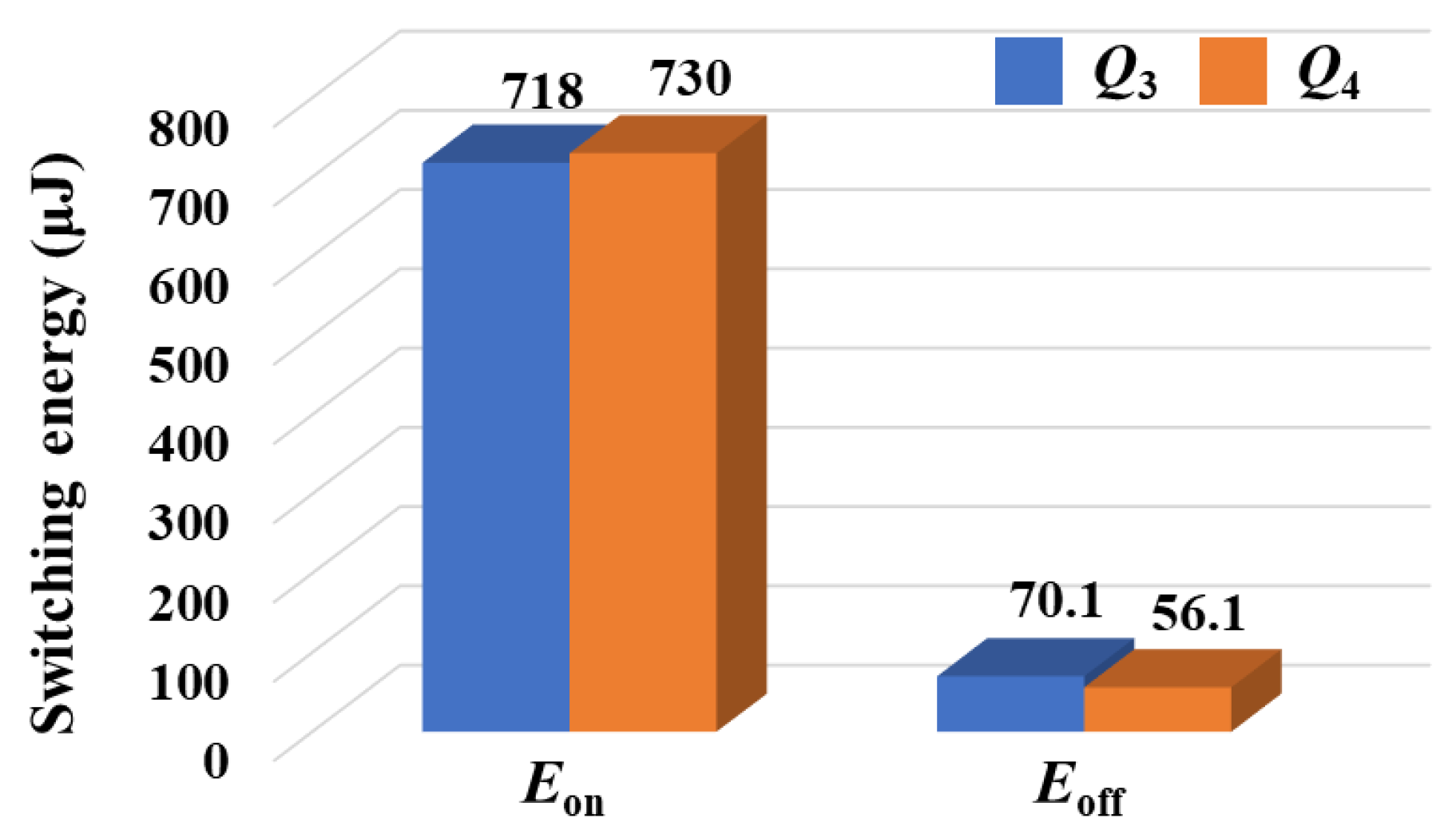
Figure 18 shows the calculated switching energies of Q
3 and Q
4 based on the experimental results in
Figure 17. The turn-on energy Eon of Q
3 is 718 μJ, and the turn-off energy Eoff of Q
3 is 70.1 μJ; therefore, the total switching energy
Etot of Q
3 is 788.1 μJ. By the same principle, the
Etot of Q
4 is 786.1 μJ. The total switching energy error between the two devices is only 0.25%, which indicates that the proposed switching power module has excellent current-balancing performance through the symmetry of the gate and power loop inductances without additional components.
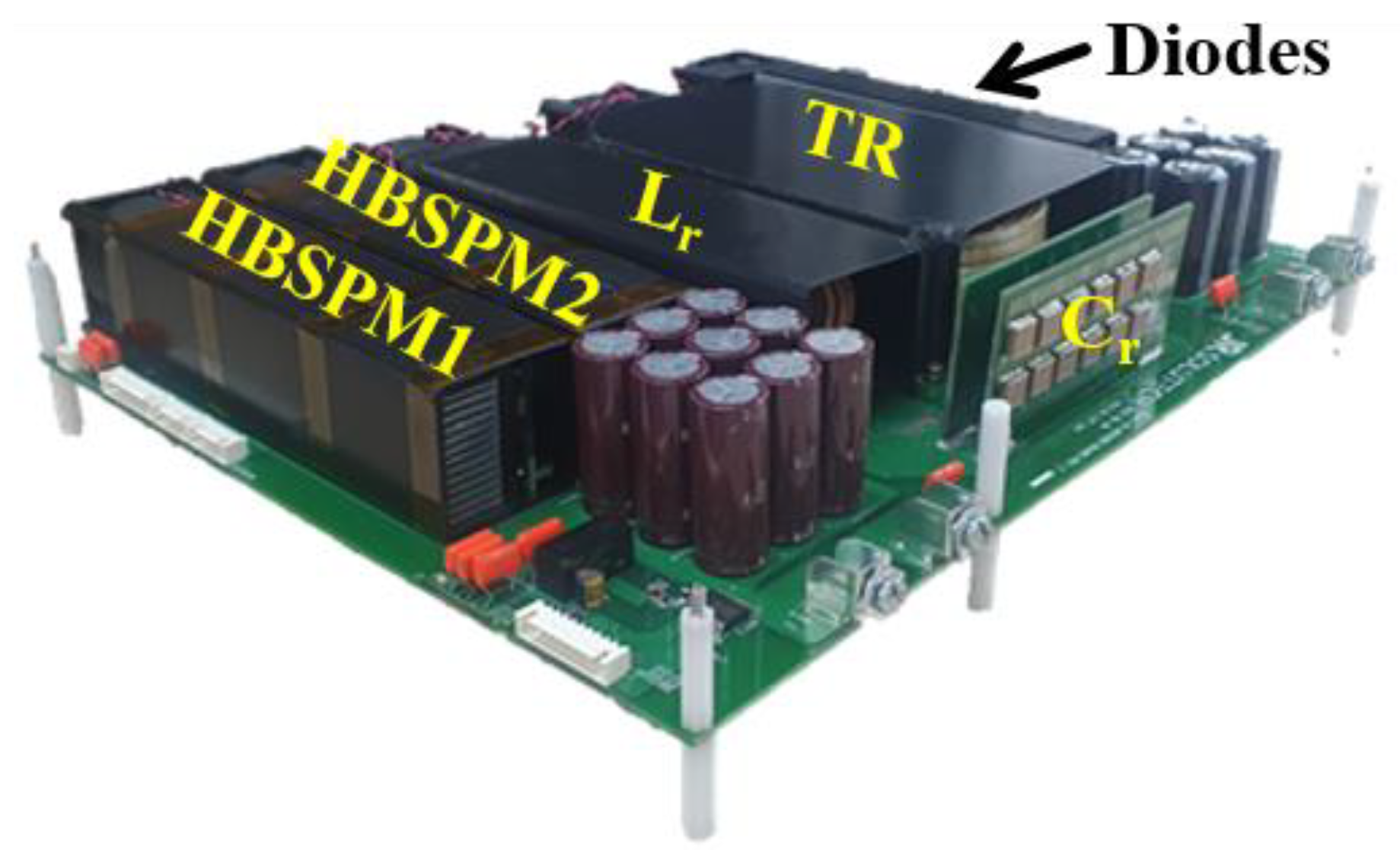
Figure 19 shows that a full-bridge LLC resonant converter is designed using the proposed HBSPM to verify current-balancing at the steady state. The full-bridge LLC resonant converter consists of two HBSPMs, a resonant inductor
Lr, a resonant capacitor
Cr, a transformer TR, and rectifier diodes. The system parameters of the LLC converter are presented in
Table 4.
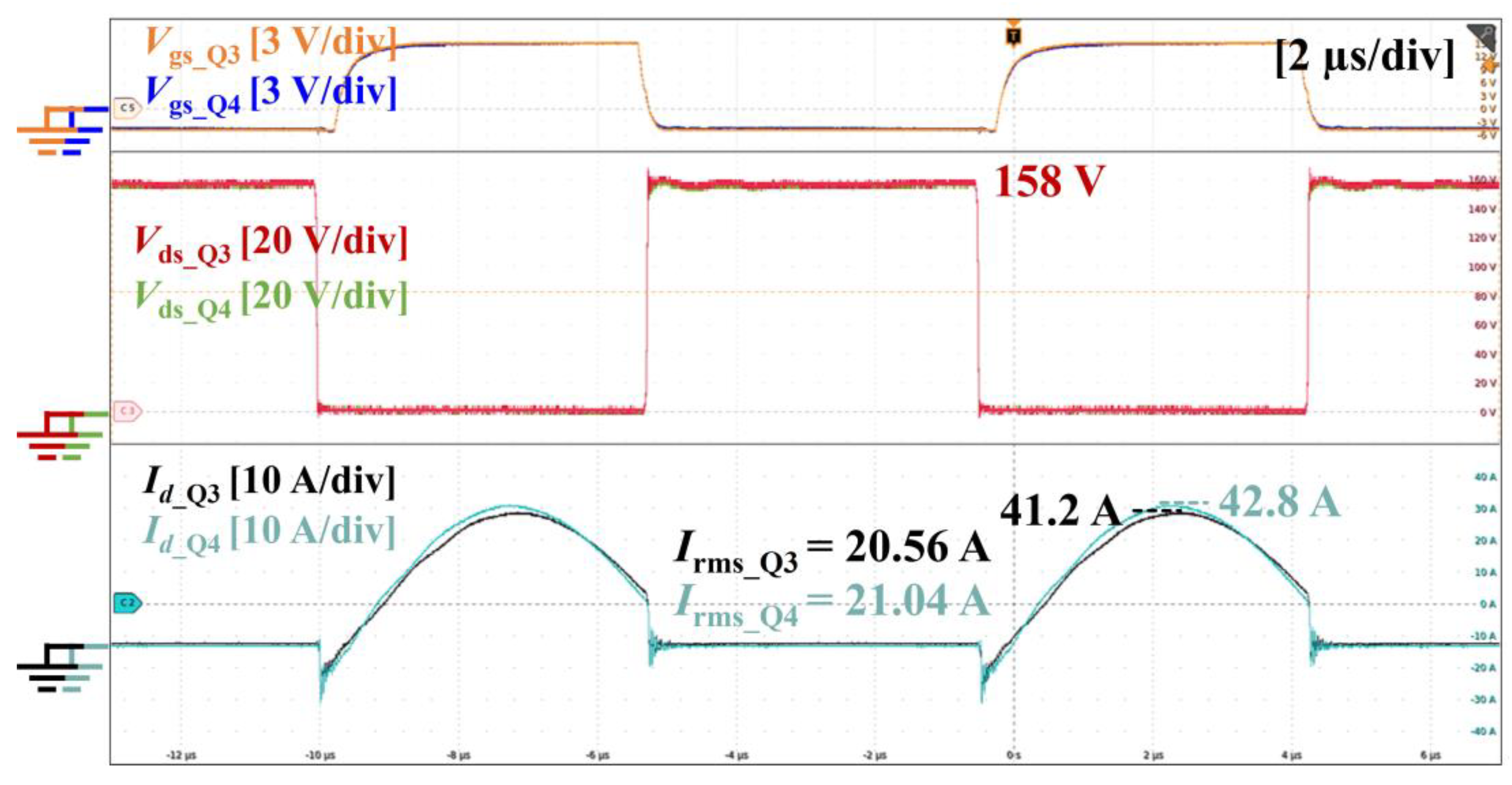
Figure 20 shows the
Vgs,
Vds, and
Id of Q
3 and Q
4 in the steady state of the LLC resonant converter. Similar to the results in
Figure 17, the
Vgs and
Vds of the two devices are almost the same, and there are slight differences in the drain current of the two devices in the conduction period. However, the magnitude of the RMS current for each device is 20.56 A and 21.04 A, with an error of only 2.28%.
Figure 21 shows the calculated conduction loss
Pcon and the turn-off switching loss
Poff for Q
3 and Q
4 based on the experimental results in
Figure 20. The turn-on switching loss is not shown in
Figure 21 because the LLC resonant converter performs zero-voltage switching. As shown in
Figure 21, the
Pcon of Q
3 is 13.53 W and the
Poff of Q
3 is 6.65 W; therefore, the total power loss
Ptot of Q
3 is 20.18 W. The
Ptot of Q
4 is 20.58 W by the same principle. The total power loss error between the two devices is only 1.94%.
These experimental results show that the proposed half-bridge switching power module based on parallel-connected SiC MOSFETs has excellent current-balancing performance and achieves a balance of conduction and switching losses between parallel-connected devices.
5. Conclusions and Discussion
A half-bridge switching power module based on parallel-connected SiC MOSFETs was proposed. The effect of the parasitic inductance of the gate and power loops on the switching characteristics of parallel-connected devices was analyzed. A parallel connection structure that can achieve the symmetry of the gate loop while minimizing the magnitude of inductance was proposed. Based on the proposed parallel connection structure, a half-bridge structure that can achieve the symmetry of the power loop was also proposed. In addition, the proposed switching power module can improve the power density of the power converter by not only achieving symmetry but also enabling a heatsink-integrated design. The symmetry of the proposed switching power module was verified by measuring the gate and power loop inductances using ANSYS Q3D. The double-pulse test results showed excellent current-balancing of the proposed switching power module. Furthermore, the parallel-connected devices of the proposed switching power module exhibited only a 1.94% power loss error in the resonant converter experiment.
The proposed HBSPM effectively suppresses current imbalance by balancing the parasitic inductance of the PCB through a symmetrical structure. However, the impact of parasitic inductance from passive and active devices other than the PCB remains a challenge to be resolved. In this study, the gate loop inductance imbalance was mitigated by using individual gate resistance, but applying the same method to the power loop is challenging. While there are existing solutions for current-balancing, many of them face technical limitations, such as a trade-off between current-balancing and switching characteristics. These challenges can make it difficult to achieve optimal performance in high-power applications. Therefore, future research is necessary to address the imbalance caused by the parasitic inductance of packages in power loop.
Furthermore, since the proposed structure is based on the Transistor Outline(TO) package, directly applying it to the Surface Mount Device(SMD) package is difficult. Nonetheless, the methodology for balancing the current remains the same. By ensuring the symmetry of the gate loop and considering the power loop symmetry of the half-bridge structure, configuring the PCB layout can achieve good current balance performance.


 ,
, 


