1. Introduction
The field programmable gate array (FPGA) devices are widely used as function accelerators in numerous end applications. Their inherent computing parallelism and re-programmability provide a tradeoff between the processing flexibility of general-purpose processors (GPP) and the optimized performance of application-specific integrated circuits (ASIC). On top of that, their low power consumption when compared to graphical processing units (GPU) makes them appealing for numerous scenarios where the optimal computation capacity per watt is a hard system constraint. The increasing need for flexible accelerator devices has brought a new family of system-on-chip (SoC) devices that may combine in the same silicon fabric FPGA programmable logic (PL), a processing system (PS), a real-time processing unit, a small-size GPU, ASIC cores, vector-processing engines dedicated to artificial intelligence (AI) and machine learning (ML) workloads, hardwired communication cores and different built-in high-speed input/output (I/O) interfaces [
1].
The native system prototyping flow for such complex FPGA-based SoC devices requires a rigorous hardware–software co-design approach. Moreover, coherent runtime programmability is required to fully exploit the capacity of the underlying processing elements in adaptive computing use cases with dynamic workloads. To achieve this, the set of functions for each application needs to be profiled, partitioned, and distributed across the different processing elements of the FPGA-based SoC, guaranteeing their seamless on-chip interlinking and the efficient management of shared resources (e.g., preventing performance loss and deadlocks). Moreover, in systems with field upgradability requirements, uninterrupted system operation needs to be guaranteed during and after a runtime reconfiguration of intercorrelated functions targeting the different processing elements of an FPGA-based SoC. To tackle the mentioned challenges, the research community and FPGA vendors have made considerable efforts over the past years to produce different design tools, reconfigurable computing solutions, and multi-core processor management frameworks. Towards this end, mature techniques are available to enable the dynamic reconfiguration of a function hosted in a given processing element of the FPGA-based SoCs. However, this is not the case for interlinked functions which are partitioned and placed in different types of on-chip processing elements.
This work focuses on how FPGA-based SoCs can be adequately utilized in mobile network infrastructure equipment, and in concrete in open and programmable radio access networks (RAN). Programmability at the RAN level first received attention in the fourth generation (4G) of cellular networks (e.g., in the context of self-organized networks and cognitive radio use cases [
2]). Things have moved a long way since then and in the fifth generation (5G) of broadband cellular networks, agile programmable technologies have been introduced across the entire network stratum, contemplating among others software-defined networking, network slicing, network function virtualization (NFV) [
3], functional splits [
4], and adaptive software defined radio (SDR) [
5]. Given the stringent performance requirements of 5G applications in terms of latency, computing complexity, and energy consumption, the run-time reconfigurable function accelerators like the FPGA-based SoCs, are considered key processing elements for the previously mentioned 5G technology innovations. Ultra high-performance FPGA-based SoCs hosting agile function accelerators are also critical for AI-ML operations in beyond 5G distributed Edge computing architectures [
6].
In this paper, we present ReproRun framework (Reprogramming accelerated and software functions at Runtime in FPGA-based SoC devices) that was designed, implemented, and validated using popular SDR systems. ReproRun is able to apply a seamless joint reconfiguration of functions targeting both the PL and the PS parts of Xilinx FPGA-based SoCs.
The run-time reconfiguration of accelerated FPGA-based functions is a key feature that aims to truly exploit the processing flexibility of FPGA devices in the context of reconfigurable computing [
7]. The partial reconfiguration features have been following the architectural evolution of FPGA devices [
8]. However, despite the undeniable benefits of PR, its adoption on behalf of different technology stakeholders and vertical application sectors has been rather modest. The run-time spatial–temporal exploitation of FPGA compute resources requires certain applications to fulfill some strict latency requirements in order not to suffer service downtimes. Different works tried to improve the PR latency and reconfiguration control overheads [
9,
10,
11]. Another major setback for more widespread use of the PR methods is concerns related to data privacy and security when FPGA devices are used as shared computing resources in multi-tenant edge or cloud applications. Data or application security and privacy concerns have been historically addressed either through key upgrades of the native PR frameworks offered by the main FPGA vendors by including new security features, or by contributions coming from the academic community [
12,
13,
14]. However, cloud and edge computing are the domains driving the FPGA reconfigurable computing innovations, by introducing virtualized frameworks that orchestrate FPGA accelerators in 5G Cloud Environments [
15]. These efforts are valuable to increase the availability of FPGAs to virtual machines or containers and to enhance the flexibility of cloud FPGA deployments [
16,
17]. The value of FPGA computing with PR is also manifested by its adoption in different vertical sector use cases [
18,
19,
20,
21]. One of the latest research interests is to use FPGA computing and PR in those use cases where ML models need to be deployed and reconfigured on the fly [
22,
23]. Finally, run-time PR in FPGA devices is used in programmable and virtualized networking deployments [
23,
24,
25,
26] and SDR [
27,
28] infrastructures.
All the previously cited works focusing on FPGA-based reconfigurable computing use cases, share conceptual communalities with the framework presented in this paper. However, the key differentiating factor is that the reconfigurable framework presented in this paper jointly manages the run-time reconfiguration of functions featuring an interlinked software and accelerated portion in a seamless way; the former is implemented in a processor embedded in the FPGA device, whereas the latter is implemented in a given partially reconfigurable PL area. Hence, the idea of reconfiguring on the fly either the software or PL-accelerated portion of the function without affecting the availability of the other part is a notable contribution compared to the state of the art. The novelty of ReproRun is important when considering that every time more processing elements are packed in the same FPGA fabric to yield complex SoC devices with heterogeneous processing resources. As a consequence, the mindset of applying a hardware-software co-design flow in an inherently monolithic or static way is challenged when the compute capacity and elasticity of this type of device are leveraged in dynamic and adaptive computing environments. ReproRun advocates that software–hardware co-design has to be rethought to contemplate run-time procedures; its contribution can be further extended and exploited in different types of use cases not necessarily limited to SDR and 5G networking.
The remainder of the paper is organized as follows:
Section 2 states the motivation and contribution of the work;
Section 3 provides an overview of some assumptions and also the specifications that were taken into account during the development of the system;
Section 4 presents the design of ReproRun with its main components;
Section 5 provides the FPGA implementation details for the two SDR platforms;
Section 6 presents the results of the experimental validation that was conducted using the two frameworks supporting the two SDR platforms (in the first based on Analog Devices FPGA firmware and graphical tools and in the second based on the GNU radio companion and the RFNoC framework of Ettus Research);
Section 7 provides the conclusions; and finally, the
Appendix A includes detailed information of a limitation encountered in one of the two experimental platforms.
2. Motivation and Contributions
Parts of the PL area in FPGA devices could be defined as reconfigurable regions (RR) at design time. One RR can host suitably pre-compiled functions, which could be replaced or interchanged at run-time, without interrupting the operation of other functions running in the static part of the FPGA (i.e., the rest of the PL area that is not defined as an RR) or in other RRs. This procedure is called dynamic FPGA partial reconfiguration (PR), which since the 2019.2 version of the Vivado FPGA design toolchain has been enriched and rebranded as dynamic function exchange (DFX). The PL functions targeting the RR are denoted as partial bitstreams. However, the run-time update, upgrade, or replacement of interdepended functions that are split and placed in the PL and PS parts of the FPGA (or other on-chip processing elements) is hiding numerous challenges in terms of performance, availability, and security. This is exactly the key contribution of ReproRun that allows to upgrade or replace interdepended PL or PS functions at run-time without compromising the availability of other services and applications running on the chip. This is a novel top-up feature to the existing PR framework offered by AMD-Xilinx.
In our case, each partial bitstream targeting an RR of the PL area comes with its respective firmware (i.e., software functions) that runs on the PS side. In order to apply a run-time partial reconfiguration, we made use of all the related building blocks, design guidelines, and tools offered by Xilinx, and also extended, modified, and combined available reference designs.
On the PS side, we leveraged asymmetric multiprocessing (AMP) principles to manage the inter-processor communication, signaling, and resource sharing. Our work guarantees the seamless run-time update of applications running at one core of the PS without interrupting the functionality of other software processes running in the same core (i.e., the rest of the PS firmware) or the interdepended functions in its PL counterpart. This was made feasible by designing a novel computing kernel denoted as a run-time firmware reconfiguration controller (REWIRE). Hence, applications comprising a PL and a PS part can update/replace any of these components without service interruption.
Adding a run-time reconfiguration framework in FPGA-powered SDR platforms serving both the PL accelerated functions and the PS firmware, opens up many research opportunities in the field of reprogrammable 5G communication systems. For instance, ReproRun can be used as the basis of an abstraction layer that could extend NFV towards those RAN infrastructure equipment residing at the edge of 5G networks, where FPGA acceleration is paramount for serving the needs of highly demanding Edge applications. Similarly, SDR systems built to host adaptive multi-radio access technologies could use ReproRun to add, replace, or scale PS/PL functions. Adaptive RAN FS can also be supported by the ReproRun framework, adding dynamicity in the run-time placement of functions, especially when considering run-time migration scenarios from split option 7.2 to split option 7.3 [
4].
ReproRun was applied in two SDR platforms featuring different 7 series AMD-Xilinx FPGA devices, and a number of different specifications in terms of on-board components and connectivity options. This alone is an important contribution of ReproRun because it implied a different design architecture for updating or replacing the PS firmware in the two SDR platforms and for applying the PR in PL-accelerated functions. Moreover, it has proved the flexibility and versatility of ReproRun to simultaneously foster accelerated computing and agile multicore reconfiguration, tailored to FPGA device specifications, SDR hardware limitations, and specific design requirements. In this respect, ReproRun could be seen as an enabler for those Open RAN and Edge computing use cases that require field adaptive function acceleration, efficient resource orchestration, and agile split computing support.
3. Base Assumptions and Specifications
ReproRun provides a flexible and extensible run-time framework for the partial reconfiguration of FPGA devices used in popular SDR platforms. The FPGA devices embed a hardwired or soft PS which communicates with the PL using a standard embedded bus interface. Our work is based on the PR design flow of AMD-Xilinx, which makes use of the partial reconfiguration controller (PRC) intellectual property (IP) core and the internal configuration access port (ICAP) port.
It is important to highlight that we have not used the newest AMD–Xilinx dynamic function exchange (DFX) framework, the successor of the Xilinx Partial Reconfiguration flow, in order to maintain compatibility with specific firmware versions of the SDR boards of interest. Notwithstanding, the PR flow is still valid across numerous platforms featuring different FPGA devices. AMD–Xilinx provides three core documents [
29,
30,
31], on how to use the PR on its FPGA devices. On top of this, AMD–Xilinx also disposes of some key Application Notes, which help to understand the proposed reconfiguration framework. The radio frequency network on-chip (RFNoC) programming framework natively used in numerous Ettus Research SDR platforms was also used in this work; the “Getting Started with RFNoC Development” (
https://kb.ettus.com/Getting_Started_with_RFNoC_Development, accessed on 1 February 2024) Application Note underpins the dependency with the AMD–Xilinx Vivado 2017.4 toolchain version. The concrete version of RFNoC that was used in this work is the UHD_4.0.0.rfnoc-devel-161-. The designed run-time PR framework has been tested and validated in the following SDR platforms:
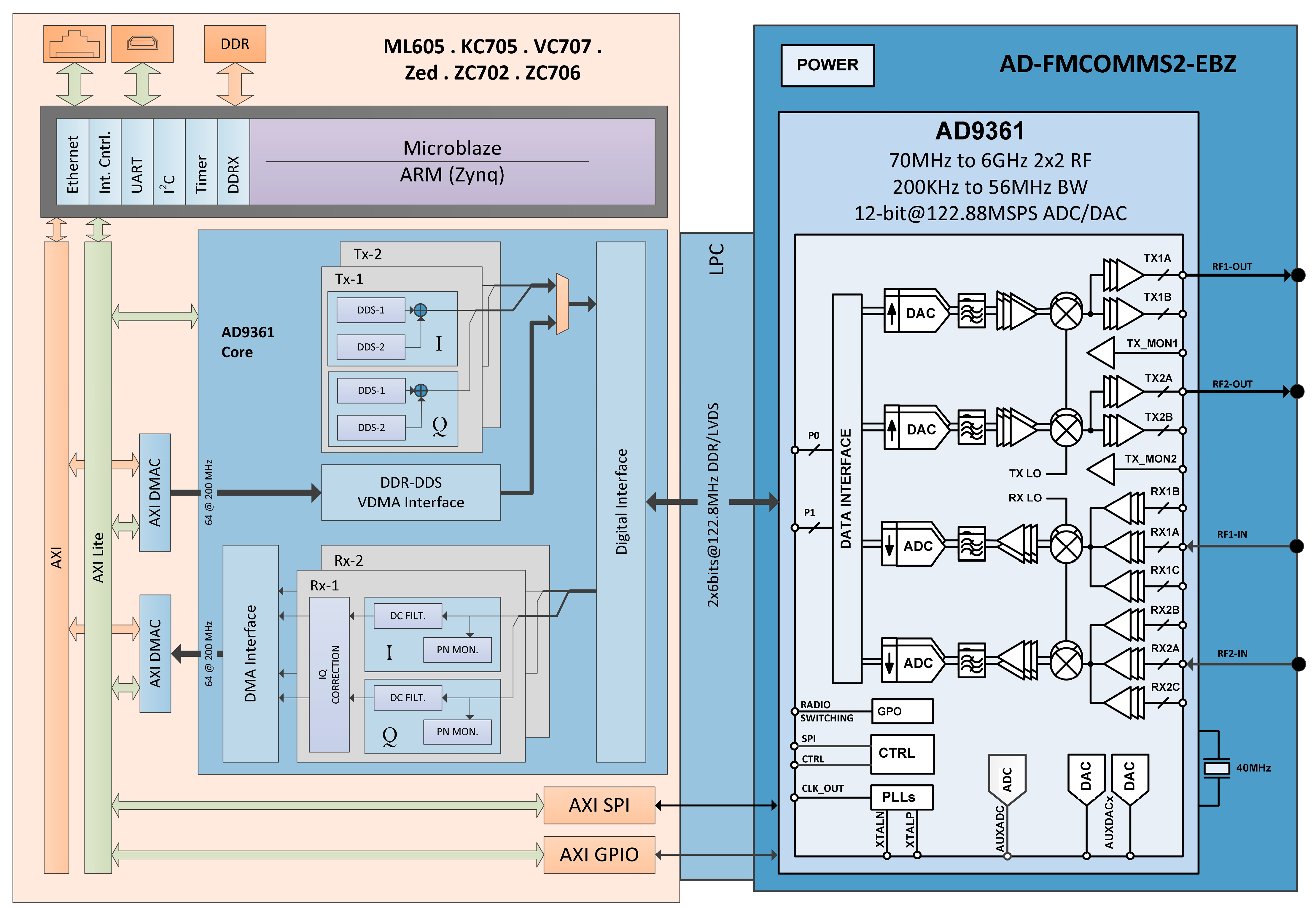
SDR1: Combines the Xilinx ZC706 development kit featuring the Xilinx Zynq XC7Z045 SoC device with the AD-FMCOMMS-2/3 evaluation board from Analog Devices. The latter features the AD9361 2 × 2 RF transceiver IC (TX band: 47 MHz to 6.0 GHz, RX band: 70 MHz to 6.0 GHz, tunable bandwidth: 200 kHz to 56 MHz).
SDR2: The Ettus Research USRP X310 SDR board, features a Xilinx Kintex 7 FPGA device. The X310 includes an agile RF transceiver module able to be programmed for a large range of RF frequencies (from 1.2 GHz to 6 GHZ, channel bandwidth of 40 MHz). The fundamental difference of this device when compared to SDR1 is the absence of a hardwired PS.
- i.
The partial bitstream that is meant to reconfigure a reconfigurable module (RM). The latter is a PL reconfigurable area defined at design time. The partial bitstreams could be digital signal processing (DSP) functions typically encountered in SDR systems (e.g., a finite impulse response (FIR) filter), or any other type of PL-accelerated functions.
- ii.
Firmware functions residing at the PS (hardwired or soft-embedded microprocessor) are essentially the piece of software that communicates, controls, and extends the operation of the partial bitstream configured in a PL reconfigurable area (e.g., a software function that programs, registers, and manages different coefficient sets of the FIR filter based on performance indicators). Each firmware function is linked with an equivalent partial bitstream, forming a bonded hardware–software application.
ReproRun provides a seamless run-time reconfiguration of both the PL and PS-based functions. The starting assumption in both SDR platforms was that the FPGA device includes functions running at the static part of the design and also a corresponding firmware running at the PS, whose operation must remain uninterrupted during and after the PR process. The FPGA devices in the two SDR platforms include one RM.
4. System Design
System design aspects included in two AMD-Xilinx Application Notes were reutilized in ReproRun. The first one [
32] shows how to use the lightweight internet protocol (lwIP) open-source TCP/IP networking stack to add networking capability to an embedded system. The lwIP was utilized to develop an echo server, a web server, a trivial file transfer protocol (TFTP) server, and receive/transmit throughput tests. The Vivado SDK provides lwIP software customized to run on the AMD MicroBlaze processor. An AMD-Xilinx Kintex-7 FPGA KC705 Evaluation Kit was used to test the system, which had to be adapted and modified for the specific design needs of ReproRun. The second Xilinx Application Note [
33] provides a software library written in C that can be used to fetch partial bitstreams over Ethernet with the help of a TFTP server. A partial bitstream discovery mechanism is provided for applications that expect their available partial bitstreams to change over time. Both applications run on a MicroBlaze Processor and help to fetch partial bitstreams that reconfigure the FPGA RM. Similarly, the Kintex-7 FPGA KC705 Evaluation Kit was used to validate the PR features. Useful features of both AMD-Xilinx Application Notes were combined, extended, and modified to serve the needs of ReproRun. For instance, the partial bitstreams and corresponding firmware objects are fetched from a remote location using the TFTP service and stored in a defined range in the external synchronous dynamic random-access memory (SDRAM) of the SDR platforms accessible by both the PL and the PS side.
ReproRun was designed to handle the seamless reconfiguration of interdepended partial bitstreams and firmware object files. This means that a partial bitstream reconfiguration in the PL does not lead to a deadlock in the firmware function associated with that partial bitstream and vice versa. In this respect, ReproRun provides consistency between RMs making sure that when a PR bitstream is swapped for another, the connections between the static design and the RM are identical, both logically and physically. This was made feasible by defining at an early design stage the interfaces between the RM and the static design. Choosing the DSP functions to be implemented inside each RM posed requirements on the type of resources an RR must comprise and, on the FPGA floor planning.
The PRC IP core guarantees a high throughput while fetching the bitstream [
34] and, accordingly, a low reconfiguration time. It also provides flexibility when managing RMs without adding any overhead to the PS (i.e., it does not compromise the execution of other tasks). Finally, the PRC IP core provides the necessary functionality to avoid deadlocks during the reconfiguration process (i.e., preserve the static part of the design) [
31] by employing isolation logic and error detection features.
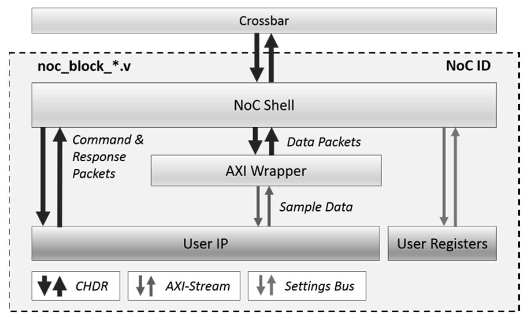
The PRC IP fetches bitstreams from a double data rate (DDR) SDRAM memory, which is specially thought to be used by the PL, and thus we call it SDRAM-PL. One of the ideas behind REWIRE and especially its part running under Linux, is that it should be able to fetch a partial bitstream and place it in a predefined memory region of the SDRAM-PL memory. Thus, SDRAM-PL must be accessible from PS as well. Then, on receiving a software trigger command the PRC core can access that bitstream and use it for partial reconfiguration. It is important to note that memory transactions between the PRC and PL-DDR are not going through the microprocessor, a fact that guarantees minimal latency during partial reconfiguration. The AXI4 interconnect was added to the design in order to arbitrate transactions from the PRC and microprocessor to the memory interface generator (MIG) controller.
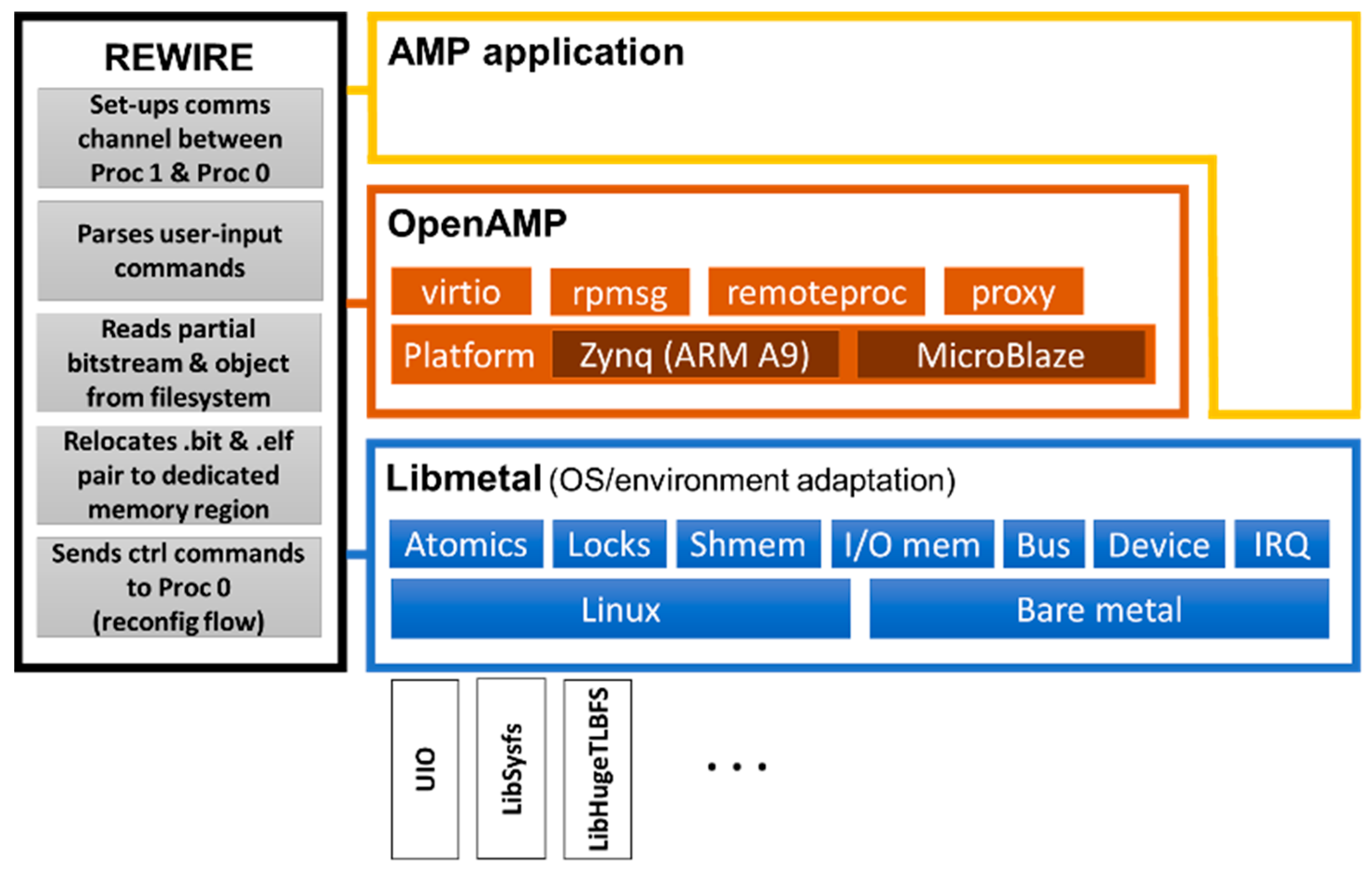
REWIRE
An AMP approach [
35] was adopted for the SDR1 exploiting the dual-core ARM A9 CPU hardwired in the Xilinx Zynq XC7Z045 device. The first core, denoted thereafter as Processor 0, needs to operate in real-time, having direct access to the hardware and deterministic processing latencies. This is mainly due to the fact that wireless transceivers typically handle high-load data processing, control several IP cores inside the PL, and need to interface with high-speed I/O protocols. The reconfigurability requirements can be considered as a control plane issue of the entire embedded design. The OpenAMP (
https://github.com/OpenAMP, accessed on 1 February 2024) solution was applied in unsupervised mode, using a bare-metal application and other firmware functions for the real-time communication functionalities in Processor 0 (slave), along with a flexible reconfigurable Linux kernel responsible for realizing administration and control functions in the second core of the ARM A9 processor denoted as Processor 1 (master).
The communication channel was built on top of the OpenAMP framework and the
libmetal library [
36]. The latter provides user application programming interfaces (API) that allow to access devices, handle device interrupts, and request memory across different operating environments (
libmetal is available for Linux, FreeRTOS, and bare-metal environments). On the other hand, OpenAMP provides life cycle management and inter-processor communication capabilities to control remote compute resources, a standalone library usable with bare-metal software environments and compatible interfacing with upstream Linux remoteproc, rpmsg, and VirtIO components. The detailed flow diagrams of OpenAMP are provided in figures 1-1 and C-1 in [
35]. REWIRE integrates OpenAMP and disposes of a set of message queues deployed over a shared memory region. The software-generated interrupts, denoted as inter-processor interrupts (IPI), were adopted for the notifications among the two cores of the ARM A9, taking care of new pending messages. This design serves to lower the response latency when compared to polling shared memory, a fact that is particularly important for time-critical routines. Proper synchronization methods were applied to avoid contention on shared resources. Xilinx reference examples [
37,
38,
39] and example applications of the OpenAMP framework were leveraged towards this end.
In the case of SDR2, the communication channel was built on top of the TCP/IP stack. As Processor 1 is represented in that case by a personal computer (PC) microprocessor, we have used a standard portable operating system interface (POSIX) compliant TCP/IP stack implementation provided by Linux. For Processor 0, we have used a Microblaze core [
40] with a bare-metal environment and the Lightweight IP (lwIP) TCP/IP stack [
32] for enabling basic networking operations. For the firmware, we used the executable and linking format (ELF) for the object and executable files since Xilinx provides a distribution of the GNU compiler and linker collection.
In order to provide further insights into the REWIRE functionality, we take as a reference FPGA architecture the one included in SDR1, because the Zynq device offers a more versatile embedded environment due to its embedded dual-core CPU. In a nutshell, the REWIRE controller manages the AMP framework and the reconfiguration procedure of the firmware functions running at the PS by performing the following tasks (
Figure 1):
establishes the communication channel between Processor 1 and Processor 0;
parses user-input commands;
reads the specified partial bitstream and object files from the filesystem;
relocates the latter into dedicated memory regions;
sends control commands to Processor 0 specifying the reconfiguration flow procedure.
We logically separated these functionalities of REWIRE into two parts. The first one is responsible for the communication between the processors, while the second one manages the firmware objects, as detailed in the following:
Part I: The inter-processor communication stack running on Processor 1 utilizes interfaces exposed to Linux user space by the OpenAMP framework. From a user-space perspective, it looks like any Linux character device, and accordingly, it provides the standard system calls-based API to interact with a device of this type. In fact, it represents an RPMsg device, which is managed by means of a series of kernel drivers implementing APIs defined in VirtIO, Remoteproc, and RPMsg frameworks of Linux. In Processor 0, the communication must be supported by the bare-metal counterpart of the mentioned frameworks. Both parts of the REWIRE, running at Processor 0 and Processor 1, interact with each other through an RPMsg communication channel. This is made possible by utilizing an external SDRAM memory for the data exchanges and IPIs for the notifications about new data transactions.
Part II: The second main part of REWIRE processes the firmware objects. As already mentioned, the ELF format is used for the object and executable files. Another part of the firmware responsible for the RR is a function or, in terms of C language a set of functions and associated structures, with a “self-contained” state. This function is mainly responsible for the initial configuration of the IP blocks inside the PL (i.e., executed once at the time when the Linux side of REWIRE notifies the bare-metal side that a new partial firmware is available). Essentially this part of the firmware must represent a single C translation unit, which after compilation will result in a single object file. In turn, the main static executable stores a pointer to the function managing the associated RR and indirectly calls this function when a new object file is delivered and processed by REWIRE. Accordingly, a predefined address of a memory region is assigned to this function pointer. This approach is applied for all sections of the object file (i.e., code, data, read-only data, and so on); in other words, a predefined amount of memory in the main executable is reserved in order to account for different firmware object deliverables. Laying out memory regions of firmware is achieved by the means of low-level GCC attributes and a linker script.
The static executable ELF file for Processor 0 is created among other files from a function main.c and the firmware dummy function dummy_prm_func.c, which simply displays a “Hello world” message. The linking of object files is done using a linker script file, which includes the following specifications:
- (1)
The size of the sections that make up the firmware function code is defined; before proceeding with reprogramming a newly produced and fetched firmware, the size compliance of the sections must be verified, because the new code will be downloaded into the memory where the bare-metal program of Processor 0 is executed. Any potential failure could block the execution of the code on Processor_0:
_PR_MODULE_FUNC_CODE_SIZE = 0x10,000;
_PR_MODULE_FUNC_DATA_SIZE = 0x1000;
_PR_MODULE_FUNC_RODATA_SIZE = 0x1000; |
- (2)
The memory direction for loading the static ELF executable file is defined as follows:
MEMORY
{
ps7_ddr_0_S_AXI_BASEADDR: ORIGIN = 0x3e000000, LENGTH = 0x00400000
ps7_ram_0_S_AXI_BASEADDR: ORIGIN = 0x00000000, LENGTH = 0x00030000
ps7_ram_1_S_AXI_BASEADDR: ORIGIN = 0xFFFF0000, LENGTH = 0x0000FE00
} |
- (3)
The sections of the firmware dummy_prm_func.o object code are defined and the pr_func_start, pr_data_start, and pr_rodata_start symbols are created:
pr_mod_func : {
. = ALIGN(0x10,000);
__pr_func_start = .;
*dummy_prm_func.o(.text)
*dummy_prm_func.o(.text.*)
. = __pr_func_start +_PR_MODULE_FUNC_CODE_SIZE;
__pr_func_end = .;
} > ps7_ddr_0_S_AXI_BASEADDR
.pr_mod_data : ALIGN(0x1000) {
__pr_data_start = .;
*dummy_prm_func.o(.data)
*dummy_prm_func.o(.data.*)
. = __pr_data_start + _PR_MODULE_FUNC_DATA_SIZE;
__pr_data_end = .;
} > ps7_ddr_0_S_AXI_BASEADDR
.pr_mod_rodata : ALIGN(0x1000) {
__pr_rodata_start = .;
*dummy_prm_func.o(.rodata)
*dummy_prm_func.o(.rodata.*)
. = __pr_rodata_start + _PR_MODULE_FUNC_RODATA_SIZE;
__pr_rodata_end = .;
} > ps7_ddr_0_S_AXI_BASEADDR |
On the host side, the dummy firmware object was compiled and linked with the mentioned main executable in order to reference its defined symbols. REWIRE creates at run-time a look-up table filled with the symbol values of a static executable and uses this table to resolve global symbol references in newly delivered firmware objects. When all necessary symbol resolutions, address fixups and the relocation and copy of code and data into the dedicated memory region are done (
Figure 2), REWIRE in Processor 1 (under Linux) notifies its bare-metal counterpart on Processor 0 that it can reprogram the RR with a new bitstream and execute new firmware code.
A complete flow diagram of ReproRun’s reconfiguration of partial bitstream and firmware objects is shown in
Figure 3.
5. Implementation
Given that the two SDR boards feature several differences apart from the different FPGA devices, they also concern other I/O and hardware specifications, a slightly different design and implementation approach was adopted for the PR solution in the two SDR boards. In fact, for the case of the SDR2 board, an important hardware limitation was encountered after applying a multi-layer debugging of the PRC core and ICAP port, taking into account guidelines [
29] such as the Pblocks recommended configuration, the global clocking rules for PR, the reset monitoring and CRC checking after reconfiguration, and other PR debugging tips. This hardware limitation deters the SDR2 board from being used in an automated run-time PR mode. For more information regarding this issue, please refer to the
Appendix A.
5.1. SDR1
In order to enable the partial reconfiguration on SDR1 we have extended the reference design provided by Analog Devices for the Xilinx ZC706 board and the AD-FMCOMMS-2/3 RF-frontend (
https://wiki.analog.com/resources/eval/user-guides/ad-fmcomms2-ebz/reference_hdl, accessed on 1 February 2024) (
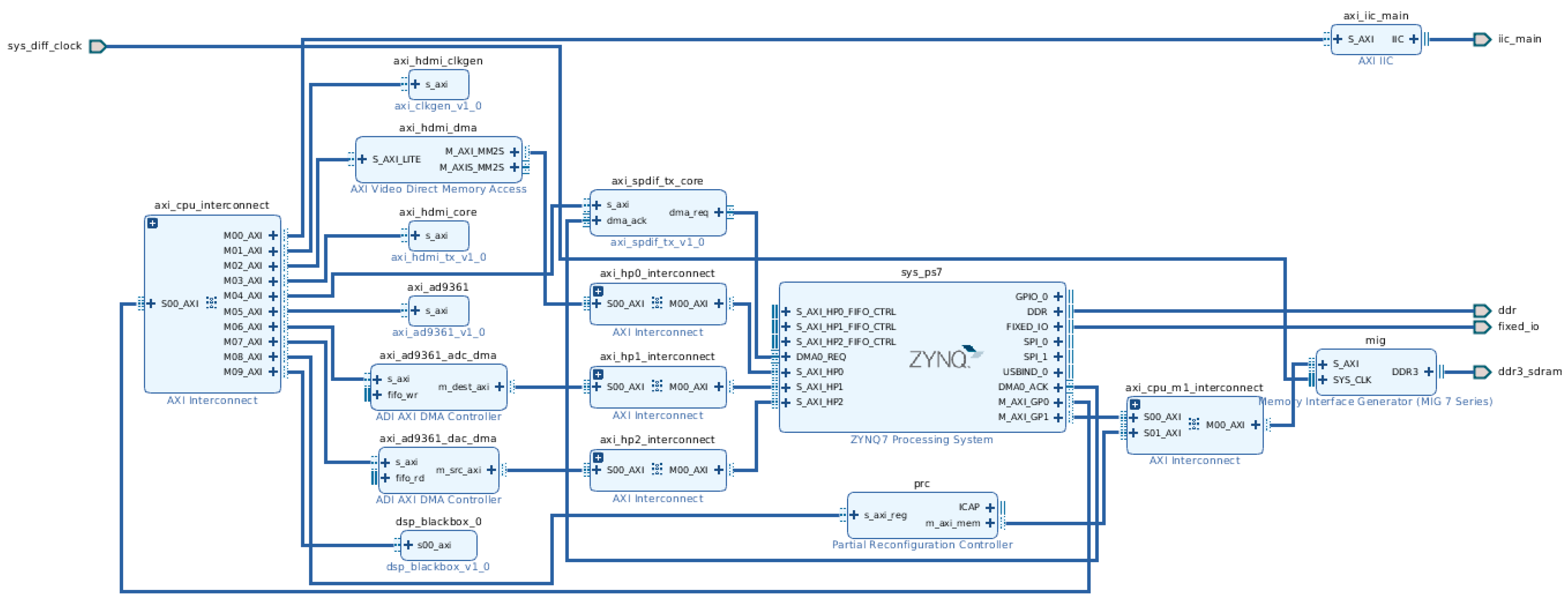
Figure 4). In the static part of the reference design, we added the PRC IP core, a wrapper around the ICAP port, a MIG IP core, a block controlling the onboard LEDs, and a DSP block, which represents the reconfigurable part of the design. The block controlling the LEDs aims to show an uninterrupted operation of the static part of the design. We also applied changes to the original blocks of the reference design to enable multiplexing of data on the digital-to-analog converter (DAC) path, to be able to switch between two sources of data (i.e., generated by the PS or the PL). The resumed version of the Vivado block design responsible for the partial reconfiguration of the PL is shown in
Figure 5.
Regarding the RR, two functions have been successfully implemented that can be replaced at run-time through the PRC controller: a direct digital synthesizer (DDS) and a 5G new radio (NR)-like signal that is cyclically play-backed. The first block reuses the Xilinx DDS IP core [
41] and allows for generating a tone signal. The second block comprises a memory array built with memory elements embedded in the FPGA fabric (i.e., block-RAMs-BRAM-) that allows for storing a 5G NR-like signal, along with a state-machine controlling the playback process of the signal. Each processing block incorporates an AXI4 slave interface; this allows the PS to write into memory-mapped registers that define the behavior of each processing block. For example, in the case of the DDS, the register sets a parameter allowing to change the synthesized frequency at run-time. Changing the processing block behavior is done in a part of the firmware responsible for the RR, which could be reconfigured by REWIRE. The reconfiguration flow of the PRC core is controlled by the static part of the REWIRE firmware running at Processor 0.
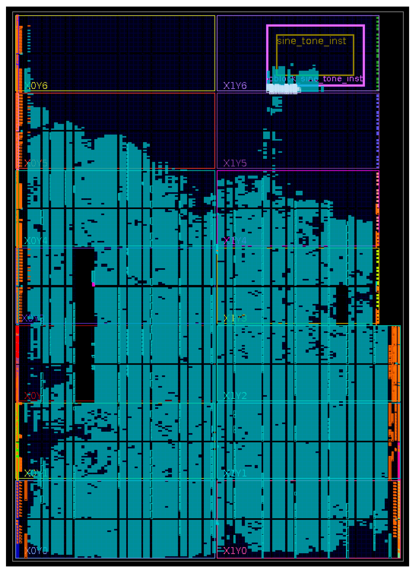
A view of the implementation results after placement and routing featuring a single RR are shown in
Figure 6 and a breakdown of the resources’ usage in
Table 1. It reveals that the FPGA implementation is low-dense and occupies a relatively small amount of the total resources, leaving the possibility of having more than one RR.
5.2. SDR2
The implementation of the system in the case of SDR2 required an elevated effort due to the inherent design complexity of the RFNoC framework. RFNoC’s main mission is to facilitate the use of hardware-accelerated DSP functions running in Ettus Research USRP devices, abstracting away their implementation complexity. The RFNoC offers likewise a hardware-in-the-loop system between a host PC and the SDR platform of interest, along with an automated software-hardware development framework tailored for SDR researchers and software engineers familiar with the GNU Radio design flow targeting USRP SDR devices. It is important to highlight that the RFNoC is not meant to be integrated with other third-party code, but solely used for its default operating scope. Extensions of the RFNoC Verilog code indeed take place within the RFNoC project but always have as an objective to abstract the low-level hardware description language (HDL) design details from the users. In the case of the PR framework proposed in this paper, several modifications and extensions of the RFNoC Verilog source code were required, with the goal of keeping its native operation intact.
When building an FPGA image for SDR2, the RFNoC framework allows configuring the two gigabit Ethernet (GigE) interfaces either as 1 GigE or as 10 GigE. The HDL firmware uses the 1 G/2.5 G Ethernet PCS/PMA and the 10 G Ethernet PCS/PMA Xilinx IP cores for the 1 GigE and 10 GigE, respectively. As far as the Ethernet medium access layer (MAC) layer is concerned (both for the 1 GigE and 10 GigE interfaces), RFNoC provides a custom Verilog implementation instead of using the relevant IP cores of Xilinx. In this context, a central element of RFNoC’s Verilog firmware is the ZPU embedded soft microprocessor (
https://github.com/pdsmart/ZPU, accessed on 1 February 2024), which interfaces with peripherals and custom Verilog glue logic via the Wishbone Bus [
42] (i.e., an open-source embedded bus standard). The Ethernet port 0 is configured to be 1 GigE serving exclusively the needs of ReproRun, whereas the Ethernet port 1 is configured to be 10 GigE serving exclusively the needs of the RFNoC firmware. While the HDL implementation of the 10 GigE link was maintained as in the original version of RFNoC, the implementation of the 1 GigE link was implemented based on the AXI 1G/2.5G Ethernet Subsystem IP core of Xilinx, which helped us to establish a bidirectional AXI4 connection between the Ethernet MAC-layer and an instance of a MicroBlaze processor (i.e., acting as Processor 0). Some necessary modifications were applied to the RFNoC Verilog code towards this end.
The use of a MicroBlaze soft processor core instead of the ZPU processor that already exists in the RFNoC HDL firmware was decided due to several design and implementation reasons. First, the MicroBlaze processor is a well-documented Xilinx IP core with detailed design guidelines and examples. The Xilinx software development kit (SDK) offers standard development tools, design automation options, and application examples for the MicroBlaze processor. In this respect, reusing the ZPU-embedded soft processor would have probably required additional effort (e.g., due to limited related documentation). Moreover, the coexistence of software functions in the ZPU processor serving both the RFNoC and ReproRun could imply the use of a real-time operating system (RTOS), increasing again the overall design effort. Hence, the MicroBlaze microprocessor core was added to accelerate and simplify the development and also to decouple the processing load of the software functions running for the RFNoC-ZPU- and ReproRun-MicroBlaze-. The MicroBlaze processor is hosting a TCP/IP stack solution, the bare-metal firmware, and a subset of the SDR1 REWIRE functionality. An optimal system design would have required a redesign of the RFNoC framework to use a single Ethernet interface for the RFNoC and ReproRun and a single embedded microprocessor running RTOS. However, such redesign falls beyond the scope of this paper.
The access to the DDR3 memory of the SDR1 had to be shared among the RFNoC and ReproRun without generating any read or write conflicts. This was made feasible by using an AXI Interconnect IP core of Xilinx and adjusting the memory-mapped address ranges for each of the two SDRAM accesses. Hence, the existing MIG [
43] configuration of the RFNoC Verilog firmware was reutilized and suitably modified.
As already mentioned before, the PRC IP provides management functions for the PR designs. Upon a trigger event initiated in the PL or PS, the PRC fetches partial bitstreams from an external memory and delivers them to the ICAP. The PRC also assists with logical decoupling and startup events, customizable per reconfigurable partition. By default, the PRC operates with RM known a priori to the controller. An AXI4-Lite register interface allows the core to be reconfigured at run-time, which means that the PRC can also be used in systems where the RMs could change at run-time. The core can be customized for a number of RMs per Virtual Socket and interface. The PRC in SDR2 was configured in the same way we did so in the case of SDR1.
The Vivado block design of the SDR2 with the key building blocks of ReproRun is shown in
Figure 7 (e.g., MicroBlaze, PRC, and AXI 1G/2.5G Ethernet Subsystem IP cores). The shared access to the SDR2 SDRAM takes place in two nested Vivado block designs. Other parts of ReproRun include blocks developed in Verilog code and a series of modifications applied to the native RFNoC Verilog source code.
The static FPGA design (static bitstream) is the combination of the modified RFNoC Verilog firmware and the HDL code of ReproRun. Two counters were developed to show the uninterrupted operation of the static bitstream (i.e., counting up and down) and their operation was mapped to a Xilinx virtual input–output (VIO) IP core to monitor them in real-time. In order to demonstrate the partial reconfiguration, we have selected the rfnoc_siggen.grc GNU radio companion (GRC) example for RFNoC (
Figure 8). This GRC RFNoC example uses a coordinate rotation digital computer (CORDIC) function to produce a sinusoid in the FPGA device of SDR2 and then passes the I and Q samples to the host PC, where the samples are processed and visualized in the GRC project (e.g., time and frequency domain analysis); some user set parameters, such as the digital gain of the signal, can be manually modified from the host PC.
The definition of the RR for the partial reconfiguration cannot be applied at the boundaries of the RFNoC blocks. By trying to do so, we noticed that when invoking RFNoC from the host it was not responsive. Hence, the RR had to be defined in one of the DSP functions of an RFNoC computation engine (CE), denoted as User IP in
Figure 8. This in turn resulted in several limitations for the PR, when for instance we want to use one RR to run different partial bitstreams (e.g., size of RR, I/O compatibility of the different partial reconfigurable functions targeting the RR). The partial bitstream was produced following the standard PR design guidelines of Xilinx and the instructions for building a user-defined RFNoC CE [
44]. For the case of the rfnoc_siggen.grc GRC example, we have applied the PR in the CORDIC function residing in this CE. The static bitstream was also modified to provide programming access to the user registers (shown in
Figure 9) from the MicroBlaze processor through an AXI protocol converter IP core (from AXI4 to AXI4Lite) and a series of state machines to manage the AXI4Lite transactions. This feature allows the modified version of REWIRE to change at run-time the gain of the signal in the rfnoc_siggen.grc example. Certain registers are monitored through VIO cores for testing and debugging purposes.
A view of the place and routed FPGA implementation (i.e., static bitstream with a single RR) and the detailed implementation results are shown in
Figure 10 and
Table 2. The FPGA implementation is medium-dense, it features various clock domains with some resources being overused (e.g., all the available BUFGs are used, making it impossible to use ILA cores to debug the system).
6. Experimental Validation
6.1. SDR1 Experimental Setup
The SDR1 setup included a mainstream laptop, the Xilinx ZC706 development board, and the AD-FMCOMMS-2/3 RF front-end evaluation board featuring the popular AD9361 RF transceiver IC (RFIC). The laptop featured an Intel Core i5-8300H central processing unit (CPU) running at 2.30 GHz, 16 GB of RAM, and a 64-bit Ubuntu 18.04.1 operating system. For the experiments with the SDR1, the following software components were installed in the laptop: Vivado System Edition 2017.4 with the Xilinx SDK, GNU compiler collection and GNU binutils, and ARM cross-compilation toolchain. The joint test action group (JTAG) and UART ports of the development board were connected to the laptop. Since Linux running on the SDR1 is basically an Ubuntu distro, we have also connected a keyboard and a monitor to it. The Ethernet port was connected to a switch in order to bring up a network connection on the SDR1 and to enable remote access through a secure socket shell (SSH) protocol session.
An overview of the experimental setup with all the functional blocks is shown in
Figure 10. The Ubuntu OS boots from an SD card. The static bitstream is programmed by the first stage bootloader, which together with other files forms the Xilinx bootable image, BOOT.BIN (also stored in the SD card). At the end of the start-up of Ubuntu, two applications provided by Analog Devices are automatically launched (i.e., the Oscilloscope and a configuration graphical user interface (GUI) for controlling the AD9361 RFIC). The connections described above allow us to flexibly configure the platform using the keyboard and the monitor. We have configured the AD-FMCOMMS-2/3 RF frontend using one of the standard 5 G configurations stored in an SD card (i.e., waveform playback); in concrete, the one supporting 1.4 MHz bandwidth signal.
The 100 Mb Ethernet port allows fetching partial bitstreams and firmware objects from a remote location and placing them in the root filesystem. As
Figure 11 shows, the REWIRE is comprised of two parts running in separate Processors: one in a Linux environment and the other in bare-metal environment under an AMP system configuration. The static part of the PL includes among others the block-controlling GPIO LEDs, which are aimed at showing the uninterrupted operation of the platform before, during, and after the partial reconfiguration (i.e., LEDs are blinking all the time). The REWIRE part running on Processor 1 accepts a few command line parameters specifying the ID of the RM to be reconfigured, the path to the bitstream, and the path to the object files. When started without command line parameters (or with incorrect parameters), the REWIRE shows the following usage message:
Usage: ./rewire -i <RM_IDX> [-b <FILE>] [-o <FILE>]
Options:
-i <RM_IDX> -specify index of RM which will be configured with a passed bitstream (-b)
-b <FILE> -specify path to a bitstream file
-o <FILE> -specify path to an object file
Examples:
(1) ./rewire -i 0 -b pr0_rm0_leds_blink.bin -o blinking_freq.o
Description:
Load .bin into PL DDR and write its size and address to a PRC config register associated with RM0. Do the FPGA PR reconfiguration, FW reconfiguration and finally jump to a new FW code.
(2) ./rewire -i 1 -b pr0_rm1_leds_shift.bin -o leds_shift_config.o
Description:
Do the same using different input files, but associate bitstream with RM1
(3) ./rewire -i 0 -o blinking_freq_slow.o
Description
Program FPGA PR area with RM0 bitstream (preloaded) and execute specified.o firmware
(4) ./rewire -i 1
Description:
Program FPGA with RM1 bitstream (do not perform FW reconfiguration) |
As can be seen above, providing a path to the partial bitstream and object file is optional. As long as different configurations are initially loaded for different RMs, REWIRE allows to switch between them specifying the ID of the RM to be used in the reconfigurable region. Of course, the described functionality must be supported by the other part of the REWIRE running in the bare-metal environment. Processor 1 sends to Processor 0 a reconfiguration message complying with the predefined format known to both processors. Depending on the user’s input, this message may contain the information about the new bitstream to be reprogrammed and in particular (i) its size and the SDRAM address where it has been loaded; (ii) what RM must be associated with this bitstream; (iii) whether the firmware has been reconfigured and thus must be executed after the PRC IP core finishes its task.
The effect of programming a new partial bitstream and/or reconfiguring the firmware can be observed in the ADI Oscilloscope or in the spectrum analyzer connected to the RF output port of the AD-FMCOMMS-2/3. The following steps produce the output of ReproRun:
On the bootup of the SDR1, we need to program the filter coefficients with a 1.4 MHz 5 G NR-like config file using Analog Devices IIO Oscilloscope GUI (
Figure 12) and disable outputs, i.e., the DAC path. In some tests, not disabling the transmit path at the start results in a DC component presented at the output.
We load a waveform from a set of predefined signals, using the DAC buffer output option of the IIO Oscilloscope GUI (e.g., 5GNR_5MHz signal), and we check the spectrum in IIO Oscilloscope GUI or in a spectrum analyzer connected to the TX1 port of the AD-FMCOMMD-2/3.
We open the Vivado hardware manager, and we assign the dbg_probes.ltx file in the probes.
We set the value of the VIO register from logical ‘0′ to ‘1′. This register is basically the control signal of a multiplexor that allows our custom PL block to provide data to the DAC.
As the RR is empty there is basically no output signal in the IIO Oscilloscope GUI (the power of the output signal visually decreases) or the SA.
We use the REWIRE solution to program a DDS DSP block inside RR (one of the two partial bitstreams prepared for this experimental validation):
- ○
./rewire -i 0 -b ../pr_bs/DSP_DDS.bin
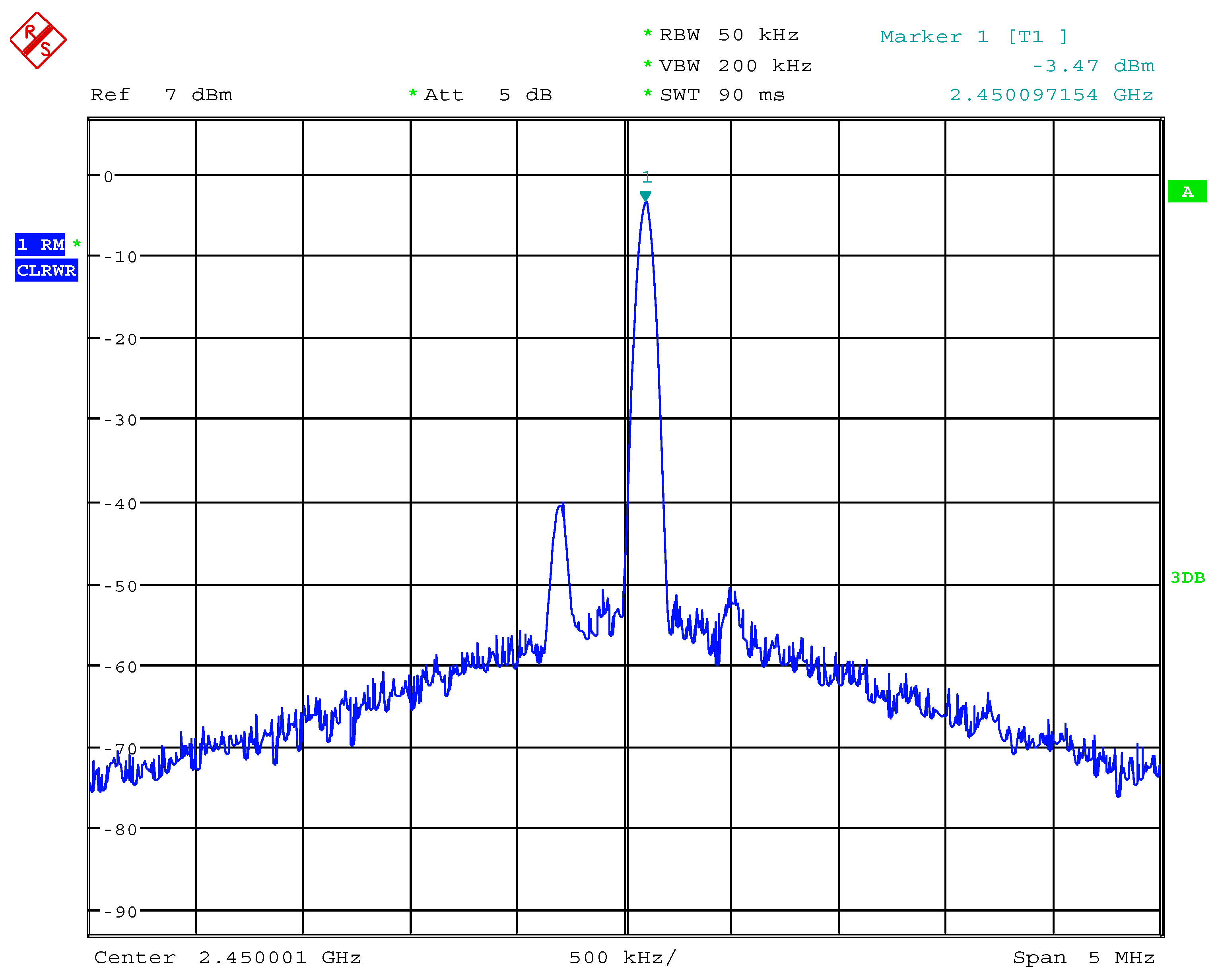
A tone signal appears in the SA, as shown in
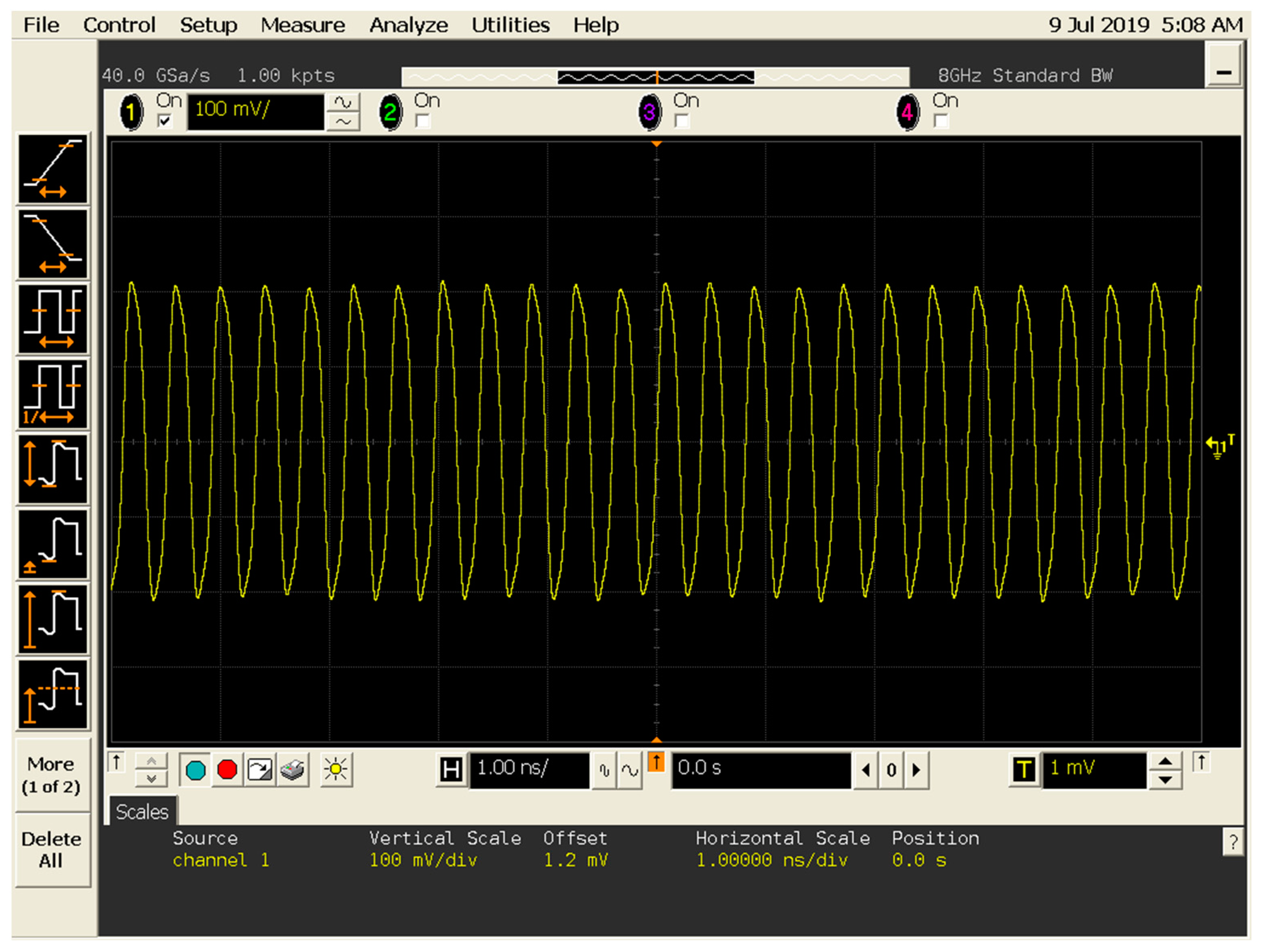
Figure 13. The frequency was set to 100 KHz by default, but it can be changed by doing a firmware reconfiguration (as explained later). You can also switch to a time-domain view in the IIO Oscilloscope GUI (i.e., by setting the resolution bandwidth parameter at 56 kHz to conveniently visualize the signal) or connect an oscilloscope equipment to the TX1 port of the AD-FMCOMMD-2/3 (
Figure 14).
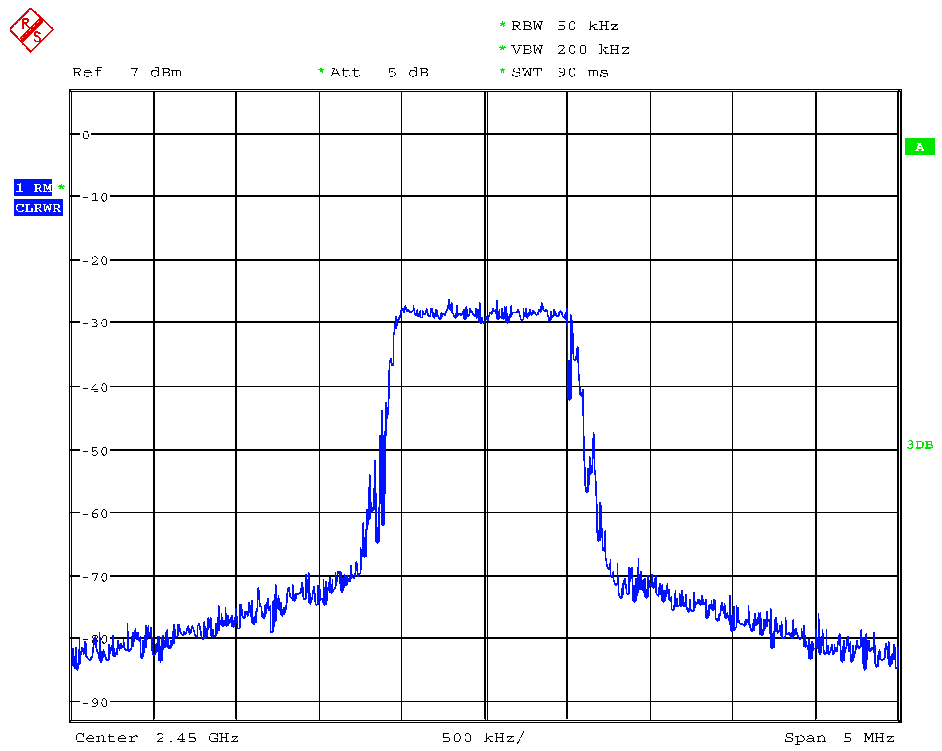
At this stage the RM can be changed in real-time by running the REWIRE again, this time using the 5 G NR-like 1.4 MHz playback block:
- ○
./rewire -i 1 -b ../pr_bs/DSP_5GNR.bin
When the reconfiguration is done, the visualized spectrum is the one shown in
Figure 15.
We can switch back to the first configuration by simply executing the following command:
As far as the firmware reconfiguration is concerned, we have built two partial firmware objects containing different DDS configurations, i.e., each one of them sets different values for a synthesized tone frequency.
By executing the following commands, the tone frequency is reconfigured on the fly:
- ○
./rewire -i 0 -o ../pr_fw/fw_dds_config_1.o
- ○
./rewire -i 0 -o ../pr_fw/fw_dds_config_2.o
In the following, we also present the example output of the REWIRE program execution, including the initial AMP configuration:
root@analog:/home/analog/reprorun/rewire# echo rewire_cpu0 > /sys/class/remoteproc/remoteproc0/firmware
root@analog:/home/analog/reprorun/rewire# echo start > /sys/class/remoteproc/remoteproc0/state
CPU0: Starting application...
CPU0: VSM 0 status:
CPU0: Try to init remoteproc resource
CPU0: Init remoteproc resource succeeded
CPU0: Waiting for events...
root@analog:/home/analog/reprorun/rewire# modprobe rpmsg_user_dev_driver
root@analog:/home/analog/reprorun/rewire# ./rewire -i 0 -b ../pr_bs/DSP_DDS.bin
-- Starting REWIRE app --
[INFO] Opening rpmsg dev...success.
[INFO] Successfully opened .BIN file
[INFO] Finished transfering bitstream to PL DDR
CPU0: Reconfiguration Msg received
[LOG] received BS_ADDR = 80A00000
[LOG] received BS_SIZE = CB7DC
[LOG] received RM_ID = 0
CPU0: VSM status after SW_TRIGGER:
Mode: ACTIVE
STATE: FULL (7)
RM_ID: 0
BS_ID: 0
ERROR: NO ERROR (0)
[INFO] CPU1: received message: RECONFIG OK!
root@analog:/home/analog/reprorun/rewire# |
6.2. SDR2 Experimental Setup
The experimental setup included a high-performance computer acting as the host featuring an Intel Core i7-7700K CPU running at 4.2 GHz, with 32 GB RAM memory. This host computer also includes a: 1 GigE interface used by ReproRun (residing in the motherboard of the PC); a dual 10 Gigabit Ethernet PCIe Card used by the RFNoC framework (i.e., one of the two interfaces); another 1 GigE interface providing the Internet access.
The host is a dual boot system (Fedora and Windows 10). In the Windows partition, we installed the Vivado System Edition 2017.4 and the Xilinx SDK. An Ubuntu virtual box (VB) machine was also installed in the Windows partition. The RFNoC framework with all its dependencies was installed in the VB (i.e., development branch, version 4.0.0).
The following communication interfaces of the USRP X310 device were connected to the host PC:
The Ethernet port 0 is configured as 1 GigE.
The Ethernet port 1 is configured as 10 GigE.
The JTAG port is used for programming the FPGA device, for early system validation, and for in-system debugging through the Vivado Hardware manager.
The two bitstreams, the static and partial one, are stored in the host PC where Processor 1 runs specific REWIRE functions. We program first the static part of the FPGA design using the Vivado Hardware Manager. As already mentioned before, the static bitstream includes two counters mapped to a VIO core in order to monitor the uninterrupted operation of the static FPGA area during and after the configuration of the partial bitstream. The other part of REWIRE runs in the bare-metal firmware of Processor 0 (i.e., MicroBlaze processor configured in the FPGA device of the X310 USRP platform). This REWIRE part receives commands from the host, specifying the name of the partial bitstream, which can be fetched from a TFTP server running at the host. The command message may also provide control information for the firmware reconfiguration. In this case, Processor 0 receives also a firmware object, which is serialized together with the rest of the commands and data forming the full reconfiguration message. The REWIRE stores bitstreams locally in the SDRAM memory of the SDR2, reprograms registers of the PRC core triggering it to start the PR procedure, and in case of success the REWIRE jumps to a new firmware if this was specified by the control commands; this firmware can access the control registers of a newly programmed CE in order to set/change the digital gain of the signal. At the same time, the rfnoc_siggen.grc RFNoC example must run at the host side, which shows the result of the reconfiguration in real time. The general overview of the experimental setup is shown in
Figure 16.
In the first stage of testing our PR solution in SDR2, none of the examples included in the RFNoC framework and running in the GRC could be used in a run-time PR context. In fact, a specific configuration-invoking procedure had to be followed to bypass the deadlocks during the PR (i.e., probably produced in the communication between the ZPU and the host PC) and bring up the correct operation of the GRC example.
The following steps produce the output of ReproRun:
The static bitstream is programmed using the Vivado Hardware Manager (
Figure 17).
We observe the operation of the VIO core that monitors two counters (up and down).
The GRC RFNoC example rfnoc_siggen.grc is launched setting before 1K in the sample rate box and the IP address in the device arguments (in our case 192.168.40.2).
Since the SigGen example includes an RR where the partial bitstream will be configured (the latter includes the CORDIC function of the example), the GRC project GUI initially does not produce an output.
We run the following command to check that RFNoC is up and running:
uhd_usrp_probe --args=“type=x300,addr=192.168.40.2”.
After receiving commands from the host, REWIRE fetches the partial bitstream making use of a TFTP server; Processor 0 also receives a firmware object.
Bitstreams are stored in the SDRAM memory of the SDR2.
REWIRE programs register the PRC core triggering it to start the PR procedure.
Once the partial bitstream is configured, we can observe in real time that the GRC GUI provides the time and frequency domain signal analysis (
Figure 18).
REWIRE jumps to a new firmware, which allows to access the control registers of the SigGen RFNoC example and modifying the digital gain of the signal.
Throughout the mentioned procedure, we can observe that the counters monitored by the VIO core operate uninterrupted.
6.3. Discussion
In broad terms, the design and features of ReproRun are served more efficiently by SDR1. The following variations are present in the two SDR platforms due to their inherent hardware and firmware features:
In SDR1, one of the cores of the ARM A9 (processor 0) hosts a bare-metal application linked with a partial bitstream and other necessary ReproRun functions that enable the run-time firmware reconfiguration, whereas the other core, Processor 1, hosts the Linux distribution of Analog Devices. The native version of the AMP framework was only applied in SDR1 since the architecture of the FPGA device in SDR2 does not favor its full use. For this reason, ReproRun was designed in a different way in the case of SDR2, since processor 0 was implemented using a MicroBlaze soft microprocessor IP core, while processor 1 was represented by a host processor. As a result, the REWIRE controller in SDR2 features a subset of the functionalities of its SDR1 counterpart.
In SDR2, it was required to integrate the PR glue logic with the RFNoC firmware without compromising its native operation. The RFNoC FPGA images running at the SDR2 can be built to include up to ten DSP functions, which then can be interconnected based on a GRC project. The latter provides a hardware-in-the-loop environment. In SDR1 Analog Devices provides the necessary HDL reference design, a Linux distribution running at the PS, and several other tools for a user to be able to prototype its own hardware-software (HW-SW) system. It is important to highlight that the user code integration in SDR1 is simpler and less dependable compared to SDR2 which uses the RFNoC framework. The native functionality of the RFNoC HDL firmware of SDR2 was modified and extended to contemplate ReproRun, resulting in an elevated code integration effort. As a general conclusion, it has to be noted that the conceptual idea of the RFNoC framework is to be used in its native version and not modified to add PR features. On top of that the SDR2 features an important limitation for being able to apply run-time PR, as it is further detailed in
Appendix A.
7. Conclusions and Future Work
In this work, we propose a novel framework that leverages the partial reconfiguration solution of AMD-Xilinx along with the AMP framework in order to provide a seamless tun-time reconfiguration of interlinked functions executed in the PL and PS portion of FPGA devices.
The heart of ReproRun is a purpose-built controller denoted as REWIRE that is able to micro-orchestrate the PL-based partial bitstreams along with their corresponding PS-based firmware. REWIRE acts as a sort of adaptive linker for the object files and interacts both with the native partial reconfiguration building blocks of AMD-Xilinx, as well as with the AMP framework. In a Zynq 7000 family of devices, REWIRE resides in the same processor core that hosts the operating system (e.g., PetaLinux), whereas the reconfigurable software application is executed as a bare-metal one in the other processor core of the FPGA system.
ReproRun automates the management of all the processes related to the AMP and partial reconfiguration functionality and allows for replacing at run-tome the software object file or its interlinked partial bitstream counterpart, without downtimes of the combined function executed simultaneously in the PS and PL. Hence, ReproRun can be considered the run-time, dynamic re-programming extension of the hardware–software co-design flow that is typically used during the implementation of an FPGA system featuring embedded microprocessors. To showcase the versatility of the proposed solution, two different types of FPGA devices were used featuring different functional characteristics, interfaces, and programming procedures. During the testing and debugging stage of ReproRun, functional differences and limitations were revealed between the two SDR boards.
The result of this combined run-time reconfiguration of hardware-accelerated and firmware functions is a novel run-time programming framework that could serve the emerging needs of programmable 6G radio and network technologies. For instance, ReproRun can be applied to FPGA-based SoC devices encountered beyond 5G disaggregated RAN architectures like the one specified by the O-RAN alliance to provide an agile reconfiguration framework of the high and low physical layer in order to achieve service requirements related to performance, low latency, and energy efficiency.
Looking forward and in the short term, it is planned to migrate ReproRun to the DFX framework using UltraScale+ Zynq as the target device family [
1]. The combination of the DFX with the isolation design flow makes this extension very promising to efficiently address the long-standing security concerns related to PR. ReproRun is also planned to be integrated into a virtualization framework and exposed to an intelligent controller at the RAN level that will cognitively take decisions for a flexible hardware–software run-time reconfiguration of network functions hosted in FPGA-based SoC devices.
Finally, considering the insecure nature of TFTP, which was adopted in this work as a simplified method to fetch partial bitstreams and object files from a remote location (i.e., accelerating the validation and testing stages of ReproRun), the goal will be to replace it with a safer networking connectivity solution. Towards this end, a secure shell (SSH) FTP solution will be leveraged to offer the full security and authentication functionality of SSH for the file transfer of the partial bitstreams and object files. On top of that and given the foreseen migration of ReproRun to UltraScale + Zynq devices, it is planned to exploit their bitstream encryption system which uses the advanced encryption standard Galois counter mode (AES-GCM) authenticated encryption algorithm. The AES-GCM encryption standard supports built-in authentication that will increase the security of the ReproRun framework, since without knowledge of the AES-GCM key, the partial bitstream cannot be modified or forged. Thus, this type of authentication will guarantee both data integrity and authenticity of the partial bitstreams. Upon authentication failure, the reconfigurable region will not start up and ReproRun will provide a fallback mechanism (i.e., a fail-safe partial bitstream will be loaded) to guarantee the availability of dependable services running at the PS side of the device.
Author Contributions
Conceptualization, N.B.; methodology, N.B. and J.R.F.; software, J.R.F., N.B. and A.R.V.; validation, J.R.F., N.B., D.L.-B. and A.R.V.; formal analysis, N.B. and J.R.F.; investigation, N.B.; resources, N.B., J.R.F., D.L.-B. and A.R.V.; writing—original draft preparation, N.B.; writing—review and editing, N.B., J.R.F., D.L.-B. and A.A.; supervision, N.B.; project administration, N.B.; funding acquisition, N.B.; All authors have read and agreed to the published version of the manuscript.
Funding
The work in this paper was supported in part by the Horizon Europe SNS JU VERGE project funded by the European Commission (Grant agreement ID 101096034), the project ORIGIN (PID2020-113832RB-C22) funded by the Agencia Estatal de Investigación MCIN/AEI/10.13039/50110001103 at the Ministerio de Ciencia, Innovación y Universidades from Gobierno de España, the project FREE6G-RegEdge (TSI-063000-2021-144) funded by the Ministerio de Asuntos Económicos y Transformación Digital from Gobierno de España, and the grant 2021 SGR 00772 funded by the Agència de Gestió d’Ajuts Universitaris i de Recerca from the Generalitat de Catalunya.
Data Availability Statement
Data is unavailable due to IP exploitation policies that apply.
Acknowledgments
The authors of the paper would like to thank Oriol Font-Bach and Pavel Harbanau for their contributions to this work. We would also like to thank Ingrid Moerman (IMEC) and her team at Ghent University (Xianjun Jiao, Wei Liu), which gave us the opportunity to develop this work in the context of the H2020 Orchestration and Reconfiguration Control Architecture (ORCA) project. CTTC was subcontracted by IMEC and entered the ORCA consortium as a third party. The experimental validation of this work was also conducted remotely in IMEC’s w-iLab.t lab and was successfully showcased during an ORCA project review conducted by EC.
Conflicts of Interest
Angelos Antonopoulos was employed by the Nearby Computing S.L. The remaining authors declare that the research was conducted in the absence of any commercial or financial relationships that could be construed as a potential conflict of interest.
Appendix A
In SDR2, we have made use of the Xilinx PRC IP core and the ICAP port to apply the run-time partial reconfiguration for a design clocked at 100 MHz. Based on the test, validation, and extensive debugging of the system, we have spotted a hardware limitation in the USRP X310 board that deters it from running the PR flow using the PRC and ICAP port. In contrast, the PR works well in SDR2 when we reconfigure the same static and partial bitstreams through the JTAG port (i.e., using the Vivado Hardware Manager). The following points describe the debugging procedure and the limitation we found in the USRP X310 board:
A process in MicroBlaze fetches the partial bitstream (.BIN file format) from the host PC via TFTP and copies the contents in the DDR3 memory.
- ○
Using a breakpoint in the executed code, we are able to verify in SDK that the contents in the DDR3 are the correct ones.
- ○
The PRC is triggered by a process in the MicroBlaze to access the .BIN stored in the SDRAM through its m_axi_mem port. Using an ILA core, we monitor that the transaction takes place without any problems.
The PRC IP core pushes the .BIN partial bitstream to the ICAP port to apply partial reconfiguration. Another ILA debug core monitors the ICAP port (
Figure A1). By reading the ICAP “O” Port bits, we check the status bits as follows (see also
Table A1):
- ○
Initial status: 1001
- ○
The ICAP receives the sync word: 1101
- ○
The ICAP receives the DESYNC command: 0101
- ○
The ‘icap_csib’ port produces a value of ‘1’: 0001
- ○
The latter means that the ICAP indicates an error directly after receiving all the data of the partial bitstream (.BIN) as it could be seen in
Figure 18 (i.e., ILA screen capture).
At that stage of debugging, we went deeper to analyze why the partial reconfiguration was not completed successfully.
- ○
In order to make the partial reconfiguration work through the ICAP interface, we need to activate the Slave SelectMAP configuration interface in our system [
45,
46].
Table 2-1 in [
45] (page 17) indicates that ports M [2:0] need to have a ‘110’ value to set the Slave SelectMAP configuration.
- ○
However, when revising the schematic diagrams of the USRP X310 board (page 9), we realized that the M [2:0] ports take the value ‘111’, which in fact is a hardwired value (thus, not reprogrammable by software).
- ○
This value must change in order to be able to use the PRC and ICAP on this SDR board.
- ○
Looking at the schematic diagrams, the only work around is to remove the R70, in which case, M2_0 will be connected to GND through the R71 resistance (i.e., likewise setting the M [2:0] with the required ‘110’ value).
Figure A1.
ILA debug core monitoring the ICAP port.
Figure A1.
ILA debug core monitoring the ICAP port.
Table A1.
the ICAP “O” Port bits [
29].
Table A1.
the ICAP “O” Port bits [
29].
ICAP “O”
Port Bits | Status Bit | Meaning |
|---|
| O [7] | CFGERR_B | Configuration error (active-Low)
0 = A configuration error has occurred.
1 = No configuration error. |
| O [6] | DALIGN | Sync word received (active-High)
0 = No sync word received.
1 = Sync word received by interface logic |
| O [5] | RIP | Readback in progress (active-High)
0 = No readback in progress.
1 = A readback is in progress |
| O [4] | IN_ABORT_B | ABORT in progress (active-Low)
0 = Abort is in progress.
1 = No abort in progress. |
| O [3:0] | 1 | Reserved |
References
- AMD. Zynq UltraScale+ Device Technical Reference Manual; AMD-Xilinx UG1085 (v2.3.1); AMD: Santa Clara, CA, USA, 2023. [Google Scholar]
- Font-Bach, O.; Bartzoudis, N.; Pascual-Iserte, A.; Payaro, M.; Blanco, L.; López, D.; Molina, M. Interference Management in LTE-based HetNets: A Practical Approach. Trans. Emerg. Telecommun. Technol. 2015, 26, 195–215. [Google Scholar] [CrossRef]
- Sabella, D.; Serrano, P.; Stea, G.; Virdis, A.; Tinnirello, I.; Giuliano, F.; Garlisi, D.; Vlacheas, P.; Demestichas, P.; Foteinos, V.; et al. Designing the 5G network infrastructure: A flexible and reconfigurable architecture based on context and content information. EURASIP J. Wirel. Commun. Netw. 2018, 2018, 199. [Google Scholar] [CrossRef]
- Font-Bach, O.; Bartzoudis, N.; Miozzo, M.; Donato, C.; Harbanau, P.; Requena-Esteso, M.; López-Bueno, D.; Serrano, P.; Mangues-Bafalluy, J.; Payaró, M. Design, implementation and experimental validation of a 5G energy-aware reconfigurable hotspot. Comput. Commun. 2018, 128, 1–17. [Google Scholar] [CrossRef]
- Gerzaguet, R.; Bartzoudis, N.; Baltar, L.G.; Berg, V.; Doré, J.B.; Kténas, D.; Font-Bach, O.; Mestre, X.; Payaró, M.; Färber, M.; et al. The 5G candidate waveform race: A comparison of complexity and performance. EURASIP J. Wirel. Commun. Netw. 2017, 2017, 13. [Google Scholar] [CrossRef]
- Kartsakli, E.; Perez-Romero, J.; Sallent, O.; Bartzoudis, N.; Frascella, V.; Mohalik, S.K.; Metsch, T.; Antonopoulos, A.; Tuna, Ö.F.; Deng, Y.; et al. AI-Powered Edge Computing Evolution for Beyond 5G Communication Networks. In Proceedings of the 2023 Joint European Conference on Networks and Communications & 6G Summit (EuCNC/6G Summit), Gothenburg, Sweden, 6–9 June 2023; pp. 478–483. [Google Scholar]
- Tessier, R.; Pocek, K.; Dehon, A. Reconfigurable Computing Architectures. Proc. IEEE 2015, 103, 332–354. [Google Scholar] [CrossRef]
- Vipin, K.; Fahmy, S.A. FPGA Dynamic and Partial Reconfiguration. ACM Comput. Surv. 2018, 51, 1–39. [Google Scholar] [CrossRef]
- Vipin, K.; Fahmy, S.A. ZyCAP: Efficient Partial Reconfiguration Management on the Xilinx Zynq. IEEE Embed. Syst. Lett. 2014, 6, 41–44. [Google Scholar] [CrossRef]
- Zamacola, R.; Otero, A.; Garcia, A.; De La Torre, E. An Integrated Approach and Tool Support for the Design of FPGA-Based Multi-Grain Reconfigurable Systems. IEEE Access 2020, 8, 202133–202152. [Google Scholar] [CrossRef]
- Valente, G.; Di Mascio, T.; Pomante, L.; D’Andrea, G. Dynamic Partial Reconfiguration Profitability for Real-Time Systems. IEEE Embed. Syst. Lett. 2021, 13, 102–105. [Google Scholar] [CrossRef]
- Elnaggar, R.; Karri, R.; Chakrabarty, K. Multi-Tenant FPGA-based Reconfigurable Systems: Attacks and Defenses. In Proceedings of the 2019 Design, Automation & Test in Europe Conference & Exhibition (DATE), Florence, Italy, 25–29 March 2019; pp. 7–12. [Google Scholar] [CrossRef]
- Dessouky, G.; Sadeghi, A.-R.; Zeitouni, S. SoK: Secure FPGA Multi-Tenancy in the Cloud: Challenges and Opportunities. In Proceedings of the 2021 IEEE European Symposium on Security and Privacy (EuroS&P), Vienna, Austria, 6–10 September 2021; pp. 487–506. [Google Scholar] [CrossRef]
- Pundir, N.; Rahman, F.; Farahmandi, F.; Tehranipoor, M. What is All the FaaS About?—Remote Exploitation of FPGA-as-a-Service Platforms. IACR Cryptol. ePrint Arch. 2021, 2021, 746. [Google Scholar]
- Pinneterre, S.; Chiotakis, S.; Paolino, M.; Raho, D. vFPGAmanager: A Virtualization Framework for Orchestrated FPGA Accelerator Sharing in 5G Cloud Environments. In Proceedings of the 2018 IEEE International Symposium on Broadband Multimedia Systems and Broadcasting (BMSB), Valencia, Spain, 6–8 June 2018; pp. 1–5. [Google Scholar] [CrossRef]
- Bobda, C.; Mbongue, J.M.; Chow, P.; Ewais, M.; Tarafdar, N.; Vega, J.C.; Eguro, K.; Koch, D.; Handagala, S.; Leeser, M.; et al. The Future of FPGA Acceleration in Datacenters and the Cloud. ACM Trans. Reconfigurable Technol. Syst. 2022, 15, 34. [Google Scholar] [CrossRef]
- Ringlein, B.; Abel, F.; Diamantopoulos, D.; Weiss, B.; Hagleitner, C.; Reichenbach, M.; Fey, D. A Case for Function-as-a-Service with Disaggregated FPGAs. In Proceedings of the 2021 IEEE 14th International Conference on Cloud Computing (CLOUD), Chicago, IL, USA, 5–10 September 2021; pp. 333–344. [Google Scholar]
- Cañas, J.M.; Fernández-Conde, J.; Vega, J.; Ordóñez, J. Reconfigurable Computing for Reactive Robotics Using Open-Source FPGAs. Electronics 2021, 11, 8. [Google Scholar] [CrossRef]
- Elhosary, H.; Zakhari, M.H.; Elgammal, M.A.; Kelany, K.A.H.; El Ghany, M.A.A.; Salama, K.N.; Mostafa, H. Hardware Acceleration of High Sensitivity Power-Aware Epileptic Seizure Detection System Using Dynamic Partial Reconfiguration. IEEE Access 2021, 9, 75071–75081. [Google Scholar] [CrossRef]
- Cervero, T.G.; Caba, J.; Lopez, S.; Dondo, J.D.; Sarmiento, R.; Rincon, F.; Lopez, J. A Scalable and Dynamically Reconfigurable FPGA-Based Embedded System for Real-Time Hyperspectral Unmixing. IEEE J. Sel. Top. Appl. Earth Obs. Remote Sens. 2014, 8, 2894–2911. [Google Scholar] [CrossRef]
- Wisniewski, R. Dynamic Partial Reconfiguration of Concurrent Control Systems Specified by Petri Nets and Implemented in Xilinx FPGA Devices. IEEE Access 2018, 6, 32376–32391. [Google Scholar] [CrossRef]
- Youssef, E.; Elsimary, H.A.; El-Moursy, M.A.; Mostafa, H.; Khattab, A. Energy-Efficient Precision-Scaled CNN Implementation with Dynamic Partial Reconfiguration. IEEE Access 2022, 10, 95571–95584. [Google Scholar] [CrossRef]
- Seyoum, B.; Pagani, M.; Biondi, A.; Balleri, S.; Buttazzo, G. Spatio-Temporal Optimization of Deep Neural Networks for Reconfigurable FPGA SoCs. IEEE Trans. Comput. 2020, 70, 1988–2000. [Google Scholar] [CrossRef]
- Almeida, L.F.; Pereira, S.S.; Domingues, J.D.; Oliveira, A.S.R.; Carvalho, N.B. Moving NFV Toward the Antenna Through FPGA-Based Hardware Reconfiguration. IEEE Commun. Lett. 2022, 27, 342–346. [Google Scholar] [CrossRef]
- Li, X.; Wang, X.; Liu, F.; Xu, H. DHL: Enabling Flexible Software Network Functions with FPGA Acceleration. In Proceedings of the 2018 IEEE 38th International Conference on Distributed Computing Systems (ICDCS), Vienna, Austria, 2–6 July 2018; pp. 1–11. [Google Scholar] [CrossRef]
- Sharma, G.P.; Tavernier, W.; Colle, D.; Pickavet, M. Dynamic Hardware-Acceleration of VNFs in NFV Environments. In Proceedings of the 2019 Sixth International Conference on Software Defined Systems (SDS), Rome, Italy, 10–13 June 2019; pp. 254–259. [Google Scholar] [CrossRef]
- Pham, T.H.; Fahmy, S.A.; McLoughlin, I.V. An End-to-End Multi-Standard OFDM Transceiver Architecture Using FPGA Partial Reconfiguration. IEEE Access 2017, 5, 21002–21015. [Google Scholar] [CrossRef]
- Hosny, S.; Elnader, E.; Gamal, M.; Hussien, A.; Mostafa, H. Multi-Partitioned Software Defined Radio Transceiver Based on Dynamic Partial Reconfiguration. In Proceedings of the 2020 IEEE International Symposium on Circuits and Systems (ISCAS), Seville, Spain, 12–14 October 2020; pp. 1–4. [Google Scholar] [CrossRef]
- AMD. Vivado Design Suite User Guide, Partial Reconfiguration; UG909 (v2017.4); AMD: Santa Clara, CA, USA, 2017. [Google Scholar]
- AMD. Vivado Design Suite Tutorial Partial Reconfiguration; UG947 (v2017.4); AMD: Santa Clara, CA, USA, 2017. [Google Scholar]
- AMD. Partial Reconfiguration Controller v1.3 LogiCORE IP Product Guide, Vivado Design Suite; PG193; AMD: Santa Clara, CA, USA, 2018. [Google Scholar]
- Sarangi, A.; MacMahon, S.; Cherukupaly, U. LightWeight IP Application Examples; XAPP1026 (v5.1); Xilinx: San Jose, CA, USA, 2014. [Google Scholar]
- Robinson, D. Loading Partial Bitstreams Using TFTP. In Xilinx Application Note: Vivado Design Suite Partial Reconfiguration Flow; XAPP1292 (v1.0); AMD: Santa Clara, CA, USA, 2016. [Google Scholar]
- Kamaleldin, A.; Mohamed, A.; Nagy, A.; Gamal, Y.; Shalash, A.; Ismail, Y.; Mostafa, H. Design guidelines for the high-speed dynamic partial reconfiguration based software defined radio implementations on Xilinx Zynq FPGA. In Proceedings of the 2017 IEEE International Symposium on Circuits and Systems (ISCAS), Baltimore, MD, USA, 28–31 May 2017; pp. 1–4. [Google Scholar]
- AMD. OpenAMP Framework for Zynq Devices; Getting Started Guide UG1186 (v2017.1), Xilinx-AMD; AMD: Santa Clara, CA, USA, 2017. [Google Scholar]
- AMD. Libmetal and OpenAMP User Guide; Xilinx User’s Guide UG1186 (v2017.4); AMD: Santa Clara, CA, USA, 2018. [Google Scholar]
- AMD. Christian Kohn Partial Reconfiguration of a Hardware Accelerator with Vivado Design Suite for Zynq-7000 AP SoC Processor; XAPP1231 (v1.1); AMD: Santa Clara, CA, USA, 2015. [Google Scholar]
- McDougall, J. Simple AMP Running Linux and Bare-Metal System on Both Zynq SoC Processors; XAPP1078 (v1.0); AMD: Santa Clara, CA, USA, 2013. [Google Scholar]
- McDougall, J. Simple AMP: Zynq SoC Cortex-A9 Bare-Metal System with MicroBlaze Processor; XAPP1093 (v1.0.1); AMD: Santa Clara, CA, USA, 2014. [Google Scholar]
- Kale, V. Using the MicroBlaze Processor to Accelerate Cost-Sensitive Embedded System Development; Xilinx White Paper WP469 (v1.0.1); Xilinx: San Jose, CA, USA, 2016. [Google Scholar]
- AMD. DDS Compiler v6.0 Xilinx LogiCORE IP Product Guide, Vivado Design Suite; PG141; AMD: Santa Clara, CA, USA, 2021. [Google Scholar]
- Herveille, O.R. Wishbone System-on-Chip (SoC) Interconnection Architecture for Portable IP Cores; Revision B.4, OpenCores. 2010. Available online: http://www.opencores.org/ (accessed on 1 February 2024).
- AMD. Zynq-7000 SoC and 7 Series Devices Memory Interface Solutions v4.2, User Guide UG586; AMD: Santa Clara, CA, USA, 2018. [Google Scholar]
- Getting Started with RFNoC Development, Application Note 823. Available online: https://kb.ettus.com/Getting_Started_with_RFNoC_Development (accessed on 1 February 2024).
- Nielson, M. Using a Microprocessor to Configure 7 Series FPGAs via Slave Serial or Slave SelectMAP Mode; Xilinx Application Note XAPP583 (v1.0); Xilinx: San Jose, CA, USA, 2012. [Google Scholar]
- 7 Series FPGAs Configuration User Guide, UG470 (v1.16) 1 February 2023. Available online: https://docs.xilinx.com/r/en-US/ug470_7Series_Config/7-Series-FPGAs-Configuration-User-Guide (accessed on 1 February 2024).
Figure 1.
A high-level overview of REWIRE.
Figure 1.
A high-level overview of REWIRE.
Figure 2.
Copying the different sections of an object file to the dedicated memory space of the PS SDRAM.
Figure 2.
Copying the different sections of an object file to the dedicated memory space of the PS SDRAM.
Figure 3.
The ReproRun flow diagram. OpenAMP’s RPmsg in Proc 1 was implemented in Linux userspace.
Figure 3.
The ReproRun flow diagram. OpenAMP’s RPmsg in Proc 1 was implemented in Linux userspace.
Figure 4.
The AD9361 hardware description language (HDL) reference design in SDR1.
Figure 4.
The AD9361 hardware description language (HDL) reference design in SDR1.
Figure 5.
The top-level Vivado Block Design of SDR1.
Figure 5.
The top-level Vivado Block Design of SDR1.
Figure 6.
The routed FPGA design in SDR1 showing the RR.
Figure 6.
The routed FPGA design in SDR1 showing the RR.
Figure 7.
The top-level Vivado Block Design of SDR2.
Figure 7.
The top-level Vivado Block Design of SDR2.
Figure 8.
The rfnoc_siggen.grc GRC example of RFNoC.
Figure 8.
The rfnoc_siggen.grc GRC example of RFNoC.
Figure 9.
The RFNoC’s Computation Engine.
Figure 9.
The RFNoC’s Computation Engine.
Figure 10.
The routed FPGA design in SDR2 showing the RR.
Figure 10.
The routed FPGA design in SDR2 showing the RR.
Figure 11.
Overview of the experimental setup of SDR1.
Figure 11.
Overview of the experimental setup of SDR1.
Figure 12.
A screen capture of some of the settings applied in the Analog Devices IIO Oscilloscope GUI.
Figure 12.
A screen capture of some of the settings applied in the Analog Devices IIO Oscilloscope GUI.
Figure 13.
The output of the AD-FMCOMMS-2/3 when the REWIRE configures the DSP_DDS.bin.
Figure 13.
The output of the AD-FMCOMMS-2/3 when the REWIRE configures the DSP_DDS.bin.
Figure 14.
A time-domain screen-capture of an oscilloscope connected to the TX1 port of the AD-FMCOMMD-2/3, when the REWIRE configures the DSP_DDS.bin partial bitstream.
Figure 14.
A time-domain screen-capture of an oscilloscope connected to the TX1 port of the AD-FMCOMMD-2/3, when the REWIRE configures the DSP_DDS.bin partial bitstream.
Figure 15.
The output of the AD-FMCOMMS-2/3 when the REWIRE configures the DSP_5GNR.bin partial bitstream.
Figure 15.
The output of the AD-FMCOMMS-2/3 when the REWIRE configures the DSP_5GNR.bin partial bitstream.
Figure 16.
Overview of the experimental setup of SDR2.
Figure 16.
Overview of the experimental setup of SDR2.
Figure 17.
The Vivado Hardware Manager programs the static bitstream and shows the monitored VIO probes.
Figure 17.
The Vivado Hardware Manager programs the static bitstream and shows the monitored VIO probes.
Figure 18.
After configuring the partial bitstream, the SigGen RFNoC example produces the correct/expected output.
Figure 18.
After configuring the partial bitstream, the SigGen RFNoC example produces the correct/expected output.
Table 1.
Implementation results of the SDR1 FPGA design where the maximum values of the FPGA resources per category are quoted in parentheses.
Table 1.
Implementation results of the SDR1 FPGA design where the maximum values of the FPGA resources per category are quoted in parentheses.
Slice LUTs
(218,600) | Slice Regs
(437,200) | F7/F8 Muxes
(109,300/54,650) | Slice
(54,650) | LUT as Logic/Memory/FFs
(218,600/70,400/218,600) | BRAMs
(545) | DSPs
(900) | Bonded IOB/IOPADs
(362/130) |
|---|
| 29,296 | 37,628 | 591/24 | 13,174 | 25,961/3335/13,390 | 18 | 71 | 223/130 |
Table 2.
Implementation results of the SDR2 FPGA design.
Table 2.
Implementation results of the SDR2 FPGA design.
Slice LUTs
(254,200) | Slice Regs
(508,400) | F7/F8 Muxes
(127,100/63,550) | Slice
(63,550) | LUT as Logic/Memory/FFs
(254,200/90,600/254,200) | BRAMs
(795) | DSPs
(1540) | Bonded IOB
(484) |
|---|
| 97,574 | 118,633 | 678/11 | 38,971 | 85,673/11,901/50,398 | 305 | 73 | 414 |
| Disclaimer/Publisher’s Note: The statements, opinions and data contained in all publications are solely those of the individual author(s) and contributor(s) and not of MDPI and/or the editor(s). MDPI and/or the editor(s) disclaim responsibility for any injury to people or property resulting from any ideas, methods, instructions or products referred to in the content. |
© 2024 by the authors. Licensee MDPI, Basel, Switzerland. This article is an open access article distributed under the terms and conditions of the Creative Commons Attribution (CC BY) license (https://creativecommons.org/licenses/by/4.0/).


 ,
, 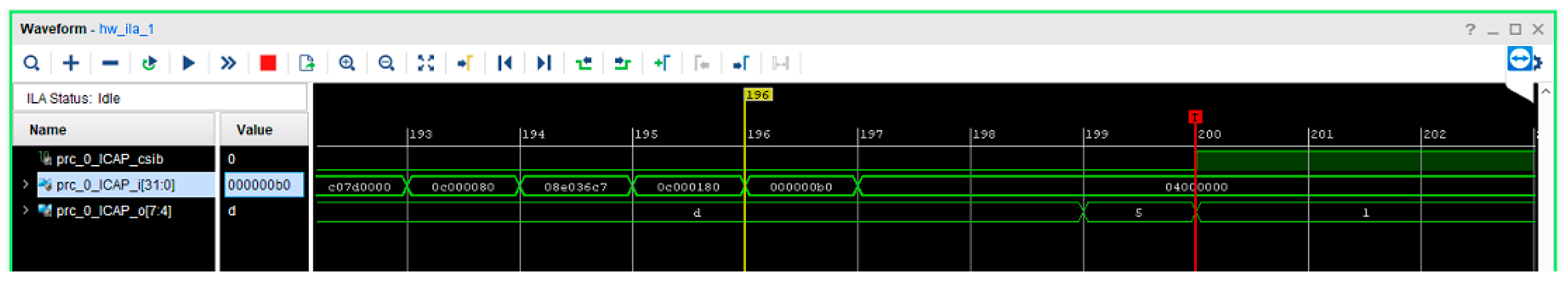

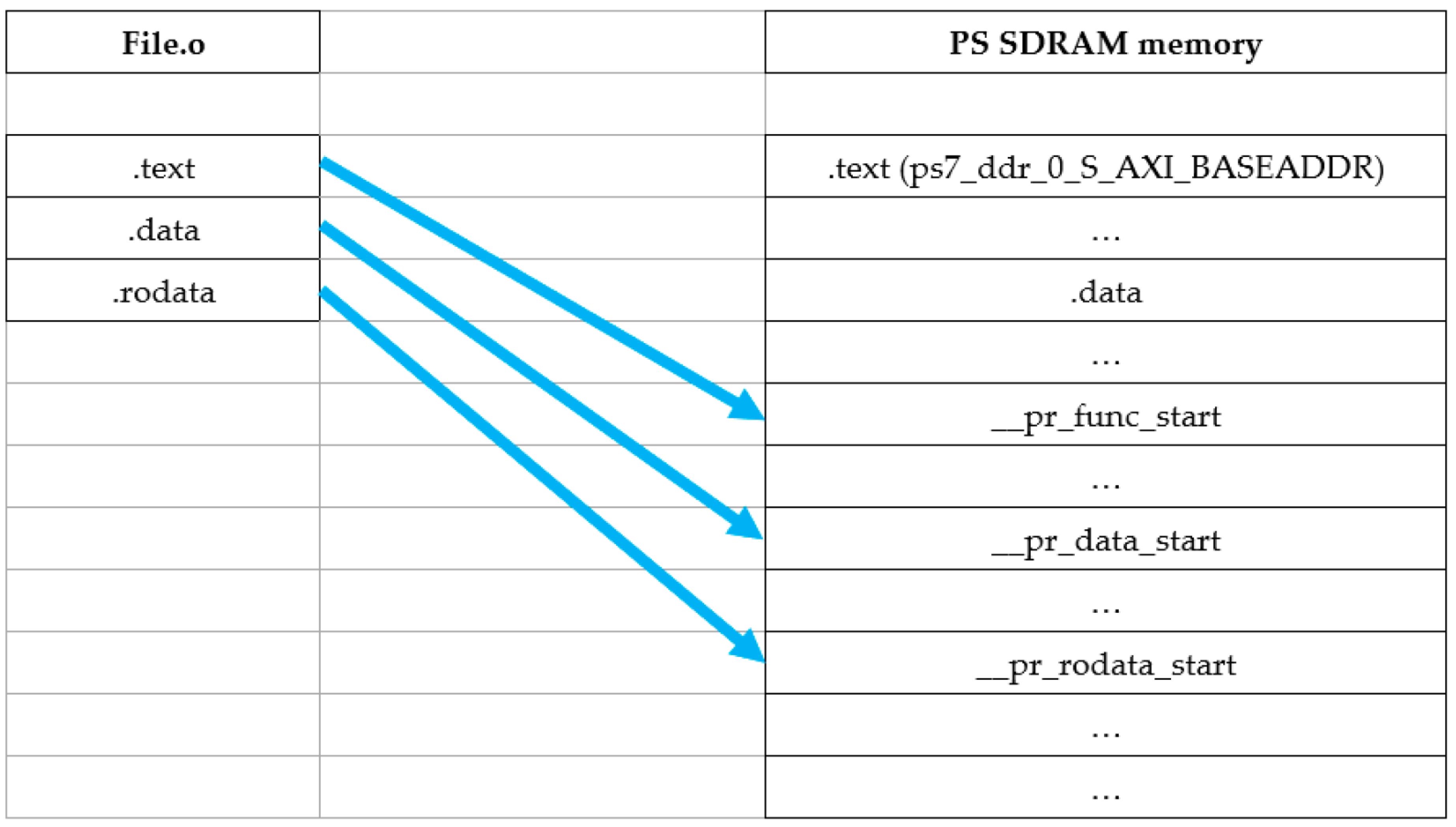
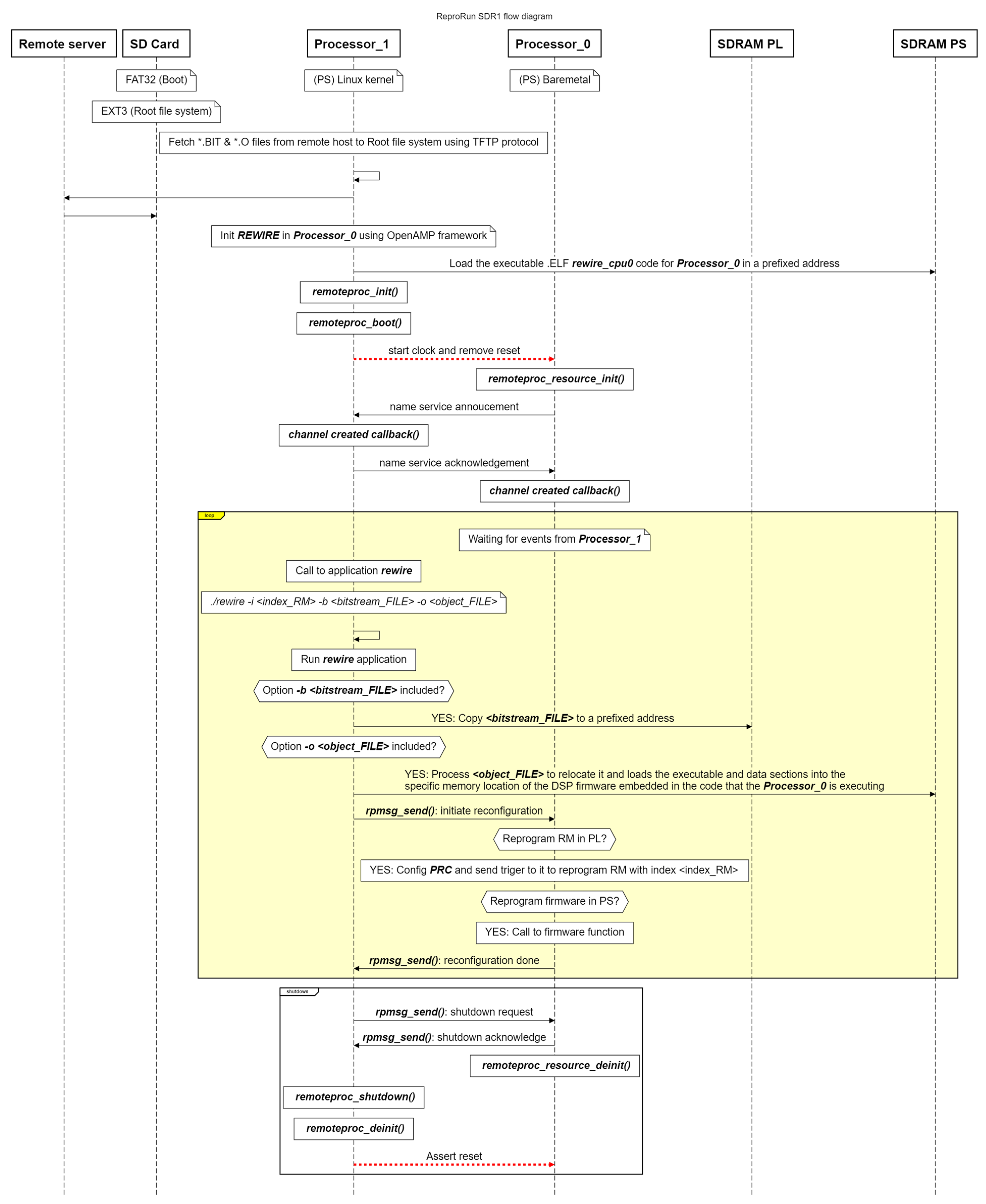
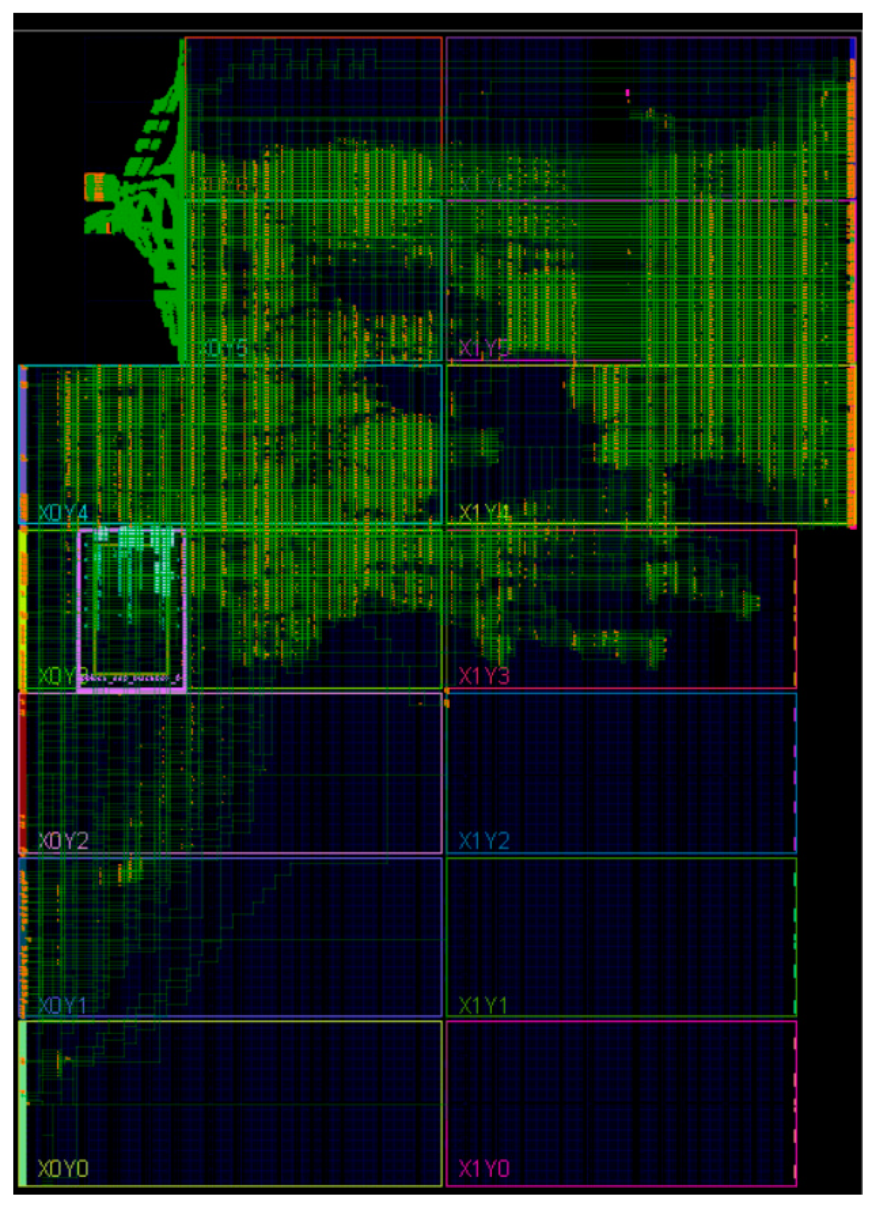
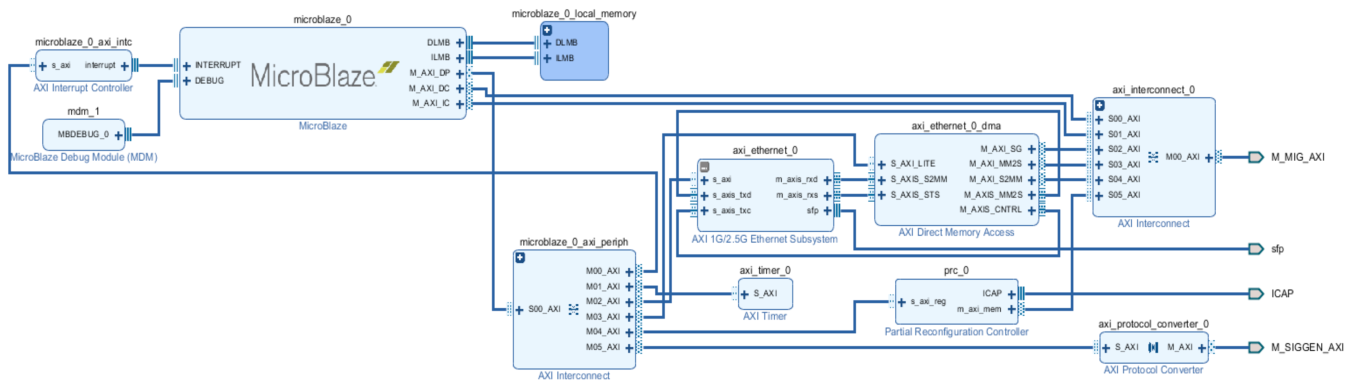
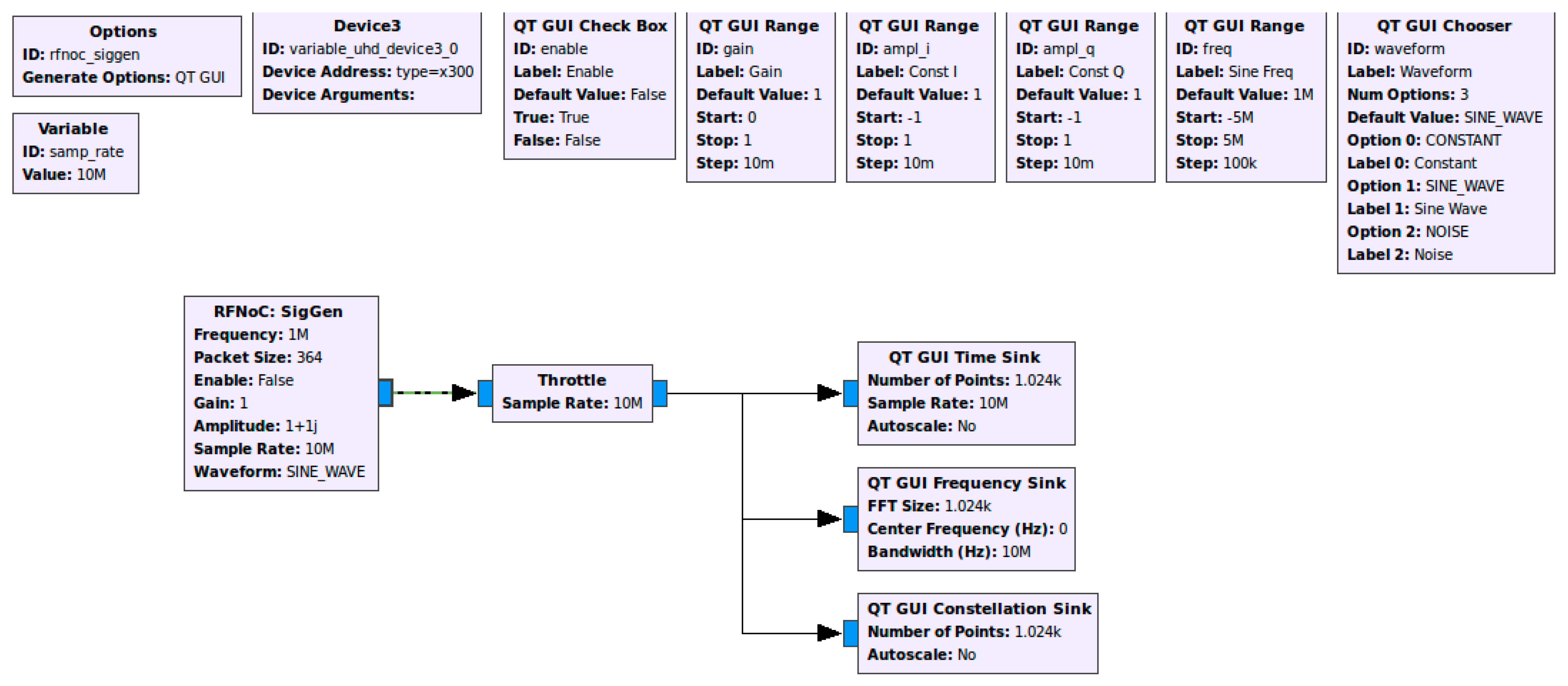
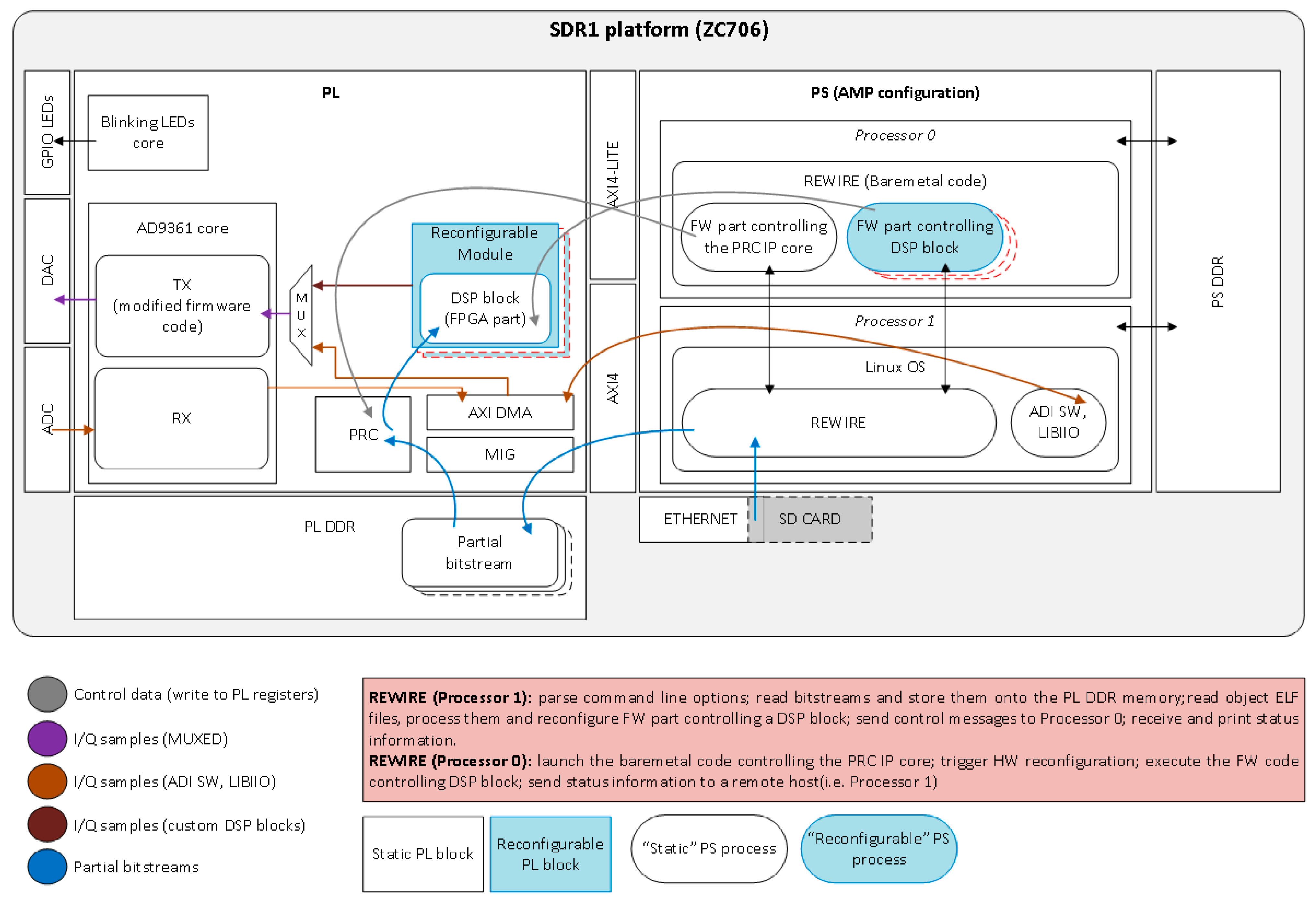
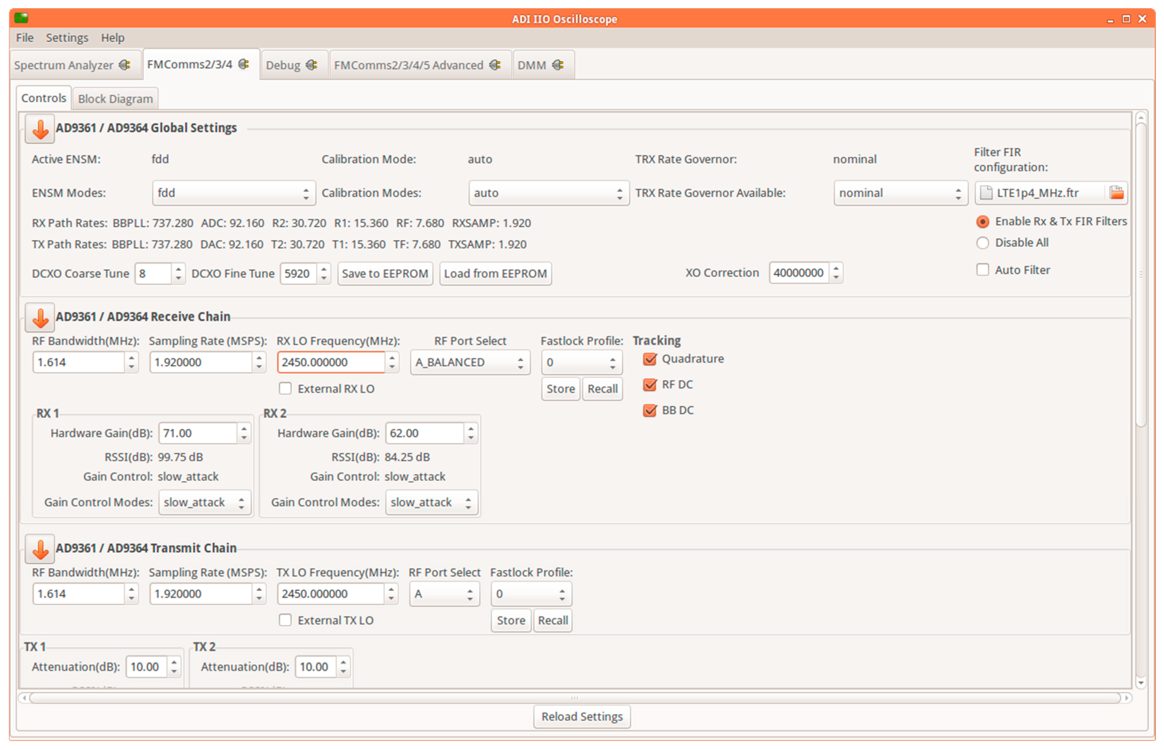
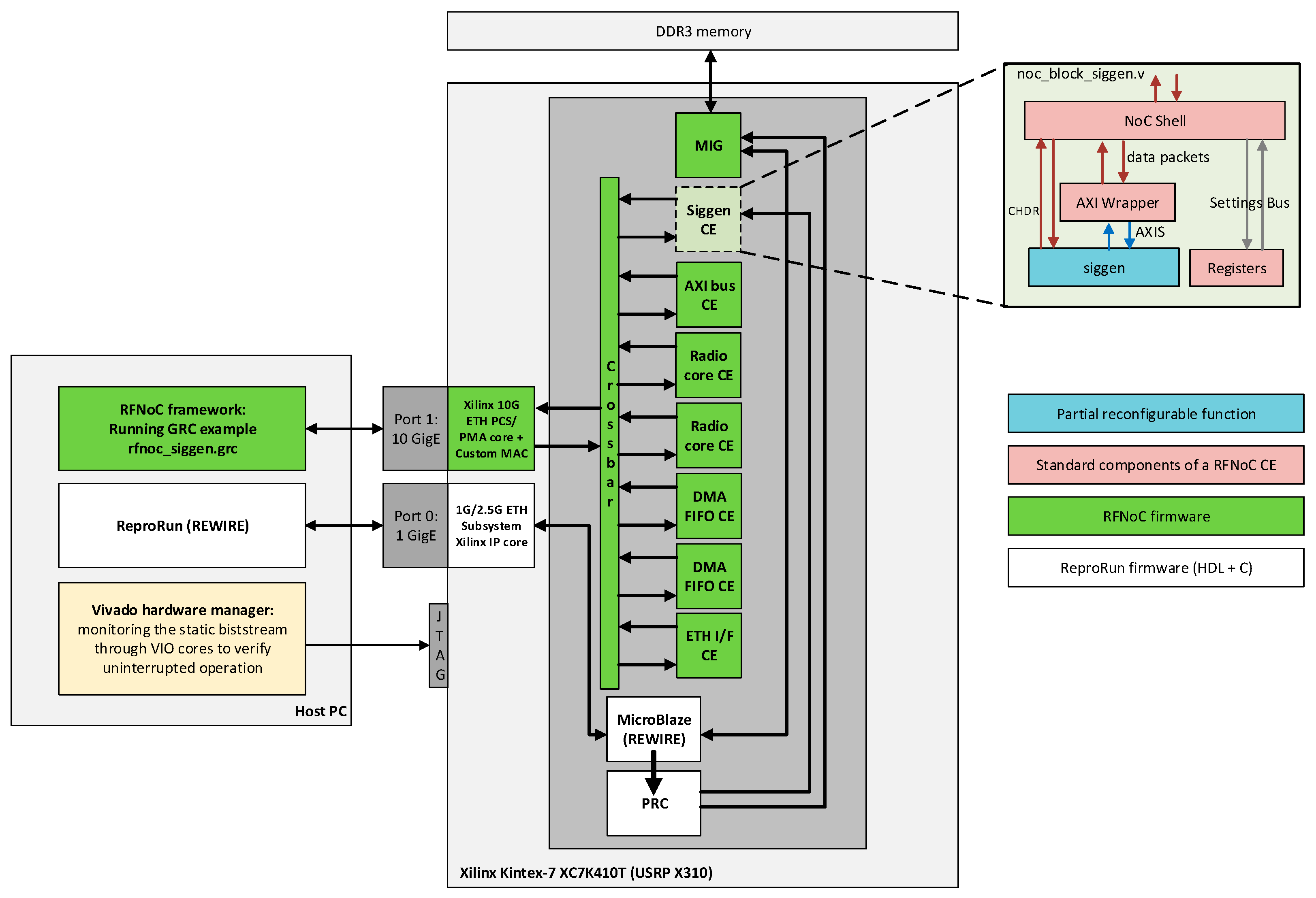
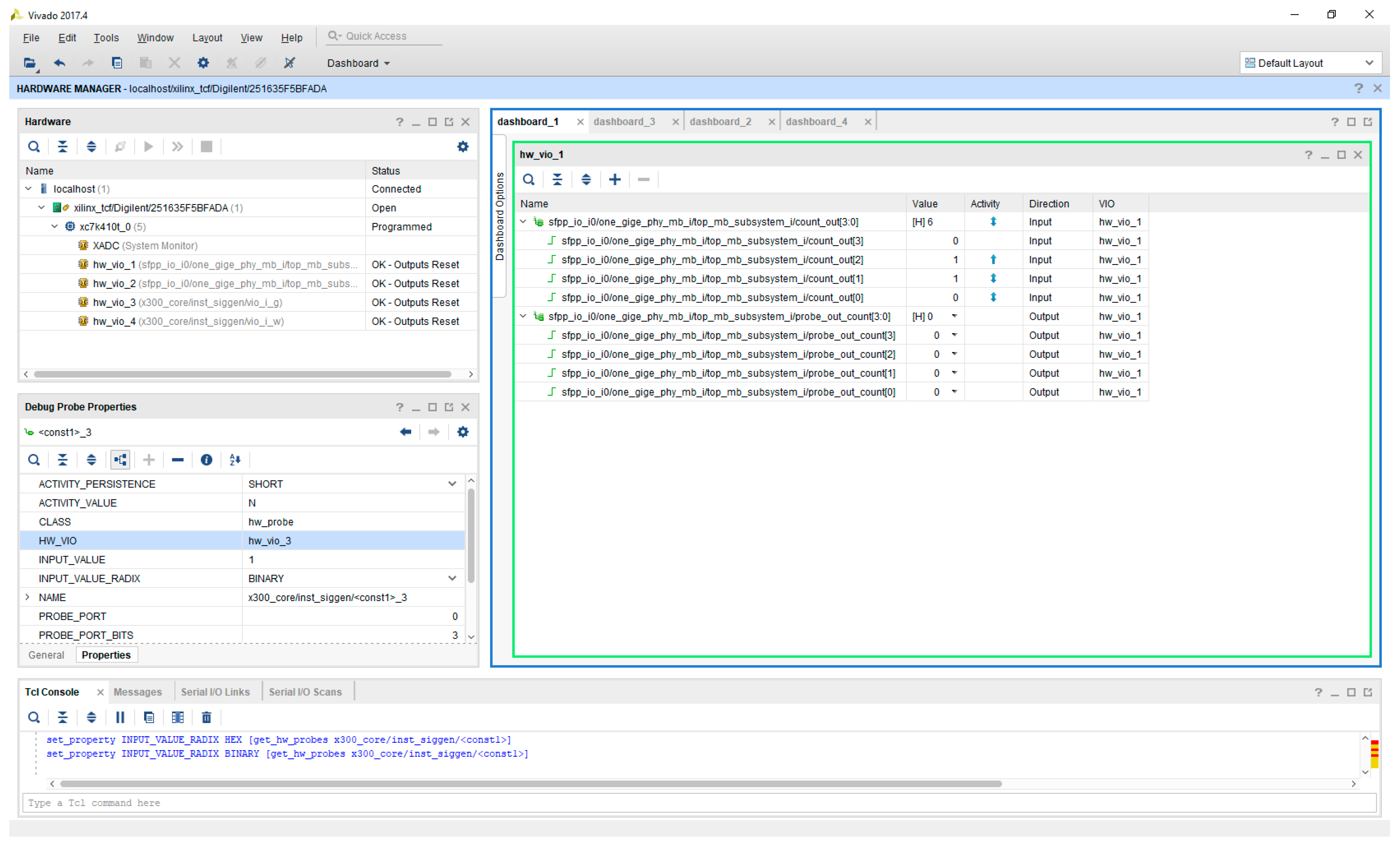
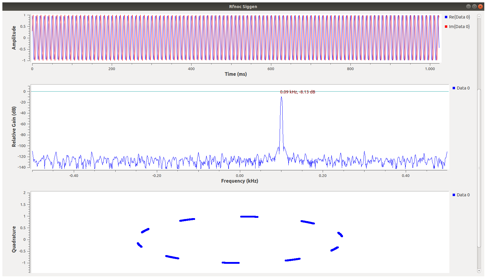