1. Introduction: Reviewing Two-Port Gains
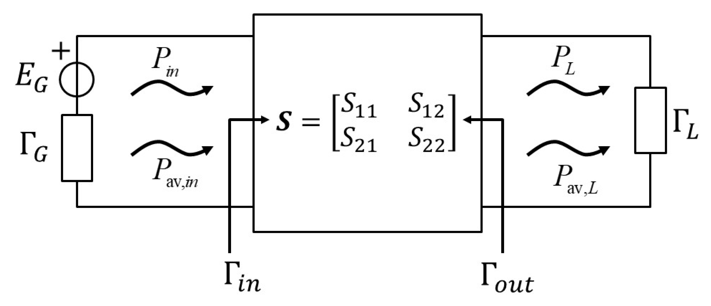
Consider a two-port of scattering matrix
, obtained through circuit analysis, CAD simulation, or experimental characterization [
1], connected at port 1 (the input port) to a generator of internal reflectance
and loaded at port 2 (the output port) by a reflectance
; see
Figure 1. All textbooks on microwave electronics agree on defining four active powers (or power spectral densities), two relevant to the input port and two to the output port, albeit with slightly different names, see, e.g., [
2] (Section 3.2), [
3] (Section 10.5), [
4] (Section 6.3), as follows:
The input power i.e., the actual power input to the network;
The input available power , i.e., the available power of the input generator;
The power actually delivered to the load, ;
The output available power , i.e., the available power from port 2.
The available power of a generator is defined as the maximum power that the generator can deliver when it is connected to a conjugately matched load.
A power gain between port 2 and port 1 can be in principle defined as the ratio of any of the output powers vs. any of the input powers. According to the Friis definition [
5], “The gain of the network is defined as the ratio of the available signal power at the output terminals of the network to the available signal power at the output terminals of the signal generator”, i.e.,
(This definition is consistent with the fact that in noise analysis all powers considered are available powers). Two years later, Roberts [
6] wrote: “We shall use the symbol for gain proposed by Friis, but shall modify his definition slightly. The gain is defined here as the ratio of the power delivered to the load impedance connected at the output terminals to the power available from the generator connected at the input terminals”, i.e.,
(In fact, Friis [
5] already noticed that his definition was “an unusual definition of gain since the gain of an amplifier is generally defined as the ratio of its output and input powers”). Finally, in 1954, Mason [
7] mentioned a “source-to-load power gain” to be interpreted probably as
; later, in 1959, Venkateswaran and Boothroyd explicitly introduced this term as the “operating power gain” [
8]. Currently, the three gains introduced are denoted by different symbols, as follows (see, e.g., [
2] (Section 3.2), [
3] (Section 10.5), [
4] (Section 6.3)):
For the sake of completeness, we recall here the expression of the gains as a function of the two-port scattering parameters and of the load and generator reflectances, see, e.g., [
4] (Sections 6.3.2, 6.3.3, 6.3.4). (Other expressions, probably more elegant, can be derived in terms of impedance, admittance, or hybrid parameters):
where
is the determinant of the scattering matrix.
If the two-port is unconditionally stable, the power transfer between generator and load can be maximized by simultaneous conjugate matching at the input and output ports, such as the input (output) two-port reflectance
(
) equaling the complex conjugate of the generator (load) reflectance,
(
). This corresponds to a maximum gain value that is obviously the same for all gains, since maximum power transfer implies that
and that
; for historical reasons, the maximum gain is often referred to as maximum available gain or MAG. However, notice that since the transducer gain depends on both the load and the generator reflectances, its maximization directly yields maximum power transfer between generator and load. Conversely, input (output) conjugate matching is additionally required to obtain the maximum power transfer when
is maximized vs.
(
vs.
). On the other hand, if the two-port is not unconditionally stable, simultaneous conjugate matching cannot be implemented, although a lower bound exists to the input and output mismatch depending on the Rollet stability factor
K [
9], as recently demonstrated by the present authors in [
10].
For the sake of completeness, we also report the gains in the so-called unilateral case, i.e., for a device with
. The past popularity of the unilateral approach to amplifier design is motivated by a number of facts. First, most active devices are almost unilateral (i.e.,
is small in magnitude). Second, unilateral design is easy and could be carried out by hand before the advent of CAD tools. Finally, devices could be made unilateral (at least in theory) by proper circuit design, see e.g., [
7]. For these reasons, gains are sometimes defined with reference to a device that is or is made unilateral, with the notation
,
,
. The MAG of a unilateral device is denoted as MUG, and the unilateral operational, available, and transducer power gains read:
A further possibility in defining two-port gain involves the concept of added power, i.e., the difference between the power delivered to the load and the input power,
. In large-signal operation, the added-power concept is the basis for the power-added efficiency parameter (see, e.g., [
4] (Section 8.2.4)). A definition and optimization of the two-port gain based on the added power has been proposed in the past by Kotzebue [
11,
12,
13] and recently exploited in [
14]. To introduce the subject, let us consider as a possible gain parameter,
(additional power gain), the ratio between the added power and the input power:
Alternative mathematical definitions of the additional power gain could involve the available input or load powers instead of the operational powers, or a combination of them. Those definitions however have never been proposed so far and seem to be of little use since the only physically meaningful definition is the one in (
1). Optimization of
is apparently straightforward since simultaneous conjugate matching results in
MAG. The maximum value of
will be therefore
. Interestingly enough, the so-called maximally efficient gain defined in [
12,
13] does not correspond to
, nor to simultaneous conjugate matching. Let us try to summarize the optimization concept proposed in the above papers. In [
13], a two-port loading condition is investigated leading to the optimization of
with constant square magnitude of the input voltage, i.e., defining:
The maximum of
g, here called
(where the subscript stands for maximally efficient, see [
12]), is defined in [
13] (Equation (
6)) in terms of the two-port admittance parameters. This maximum is achieved with the two-port load defined in [
13] (Equation (
7)); the generator is power-matched. The equations are reported here for completeness:
The parameter
g (and its maximum
) clearly is a transconductance rather than a power gain, and the input power
will depend not only on
, but also on the input reflectance or immitance of the two-port. In [
12], the optimum parameter
is reformulated, albeit in a slightly different form, as the “maximally efficient gain”,
, defined, somewhat obscurely, as “the power gain which maximizes the 2-port added power for a given value of the input port independent variable”. The parameter is defined as:
with the optimum load and generator admittance defined again as in (
3) and (
4). The same equations are reported in [
14] (Equations (1)–(3)), correcting a sign misprint in [
12] (Equation (
3)). The maximally efficient gain can also be reformulated in terms of S-parameters as:
(see [
12] (Equation (
4))) where
K is the Rollet stability factor. It is important to stress that the maximally efficient gain
does not actually correspond to the maximum additional power gain
, but rather to the operational power gain
evaluated in the optimum load condition (
3).
The relationship between the parameters
(
2) and
(
5) can be easily derived taking into account that
, where
is the two-port input admittance. We therefore have:
i.e.,
A number of advantages related to the choice of this optimization paradigm are reported in [
11,
12,
13] (this choice would be a batter compromise in terms of the amplifier large-signal saturation behavior) and in [
14] (where the technique is exploited to optimize gain-boosted amplifiers working close to the maximum oscillation frequency). Furthermore, application of the maximally efficient gain concept to high-power oscillator design was first proposed in [
15]. (In [
15], the
concept is formulated as “the power gain which maximizes the two-port added power”, and expressions are provided for the optimum load and generator reflectances).
2. Is a Fourth Gain Missing?
A fourth possibility for defining a gain indeed exists, as follows:
In this section, we intend to explore the properties of the apparent power gain
, anticipating that this parameter has some interesting mathematical properties but is of little use in circuit design, since, as the name itself suggests, it does not generally correspond to a physically realizable circuit configuration, as discussed in detail in
Section 3. First of all, we point out that the apparent gain is not independent from the other ones; indeed:
or:
Moreover, since:
this implies the following inequalities:
i.e.,
The only condition corresponding to the equal sign is when MAG.
In general, can be, according to the loading conditions, larger or smaller than MAG. The reason for this behavior is that the output available power becomes the output power in case of output matching, but setting the load reflectance accordingly changes in turn the input power. In other words, the apparent gain does not refer to a physically realizable circuit configuration unless conjugate matching is imposed at both ports.
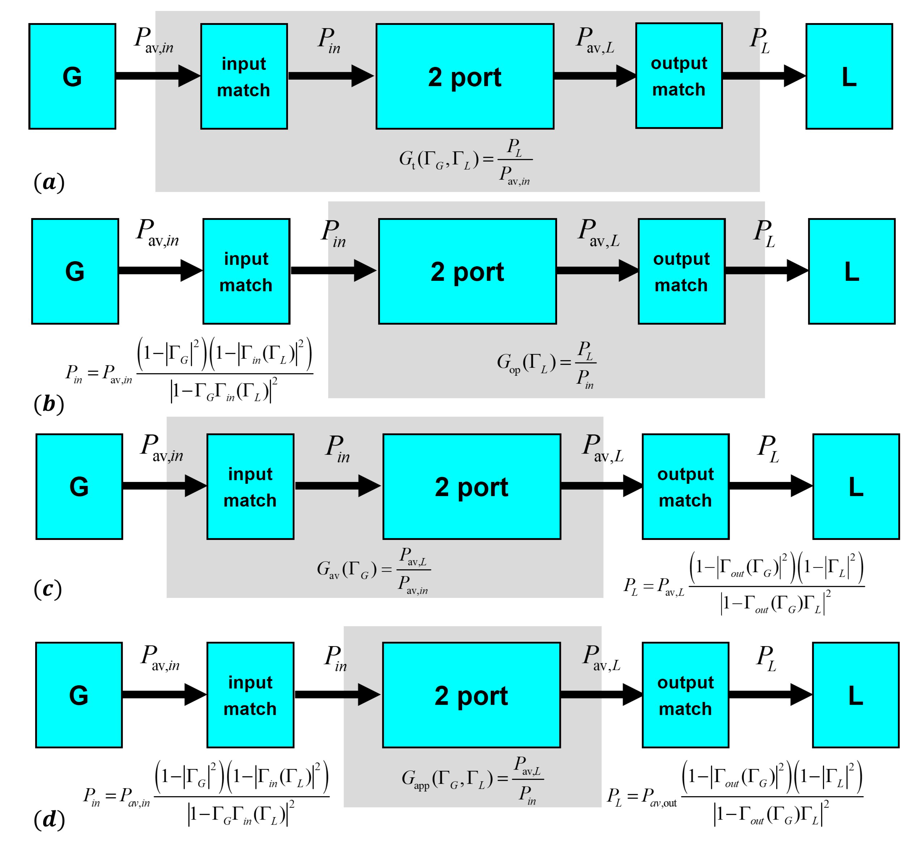
A schematic illustration of this is depicted in
Figure 2, where the maximization of power transfer between the generator
G and the load
L through reactive matching sections placed at the two-port input and output, respectively, is depicted as a block scheme. Simultaneous conjugate matching implies that the generator available power is the two-port input power and that the power delivered to the load is the two-port output available power. As shown by the grey shadowed box in
Figure 2a, this directly corresponds to the maximization of the transducer gain. Maximizing the operational gain (see the grey shadowed box in
Figure 2b) is a necessary but not sufficient condition for maximum power transfer since it does not automatically include the input conjugate matching. The same remark applies to the maximization of the available power gain (see the grey shadowed box in
Figure 2c); this time, the
output conjugate matching is not included and has to be separately implemented in order to maximize the power transfer. Finally, as shown in
Figure 2d, regardless of which condition we may impose on the apparent gain, this does not imply either the input or the output conjugate matching. However, if the input and output reactive matching sections are designed so as to obtain input and output simultaneous conjugate matching (that is, the necessary and sufficient condition for maximum power transfer), the value of the apparent gain will consistently correspond to the MAG.
We further observe that, from this scheme, it appears that an alternative to maximize the input–output power transfer by maximizing is to optimize and together, e.g., to optimize their product , or a monotonically increasing function of it.
As expected,
depends on both the load and the generator reflectances. Its explicit expression is:
Taking into account that:
we can also write:
Equation (
8) is a partial unilateral approximation of
, i.e., the term
has been approximated to unity while the input and output reflectances have been computed with the actual value of
. For potentially unstable devices,
diverges when
or
, which defines again the customary load/generator stability circles. Finally, a somewhat surprising result is obtained for a completely unilateral device (
). In such a case,
and
, and therefore:
In other words, for a unilateral device
is constant, independent on the load conditions, and equal to the maximum unilateral gain. A consequence of (
9) is that, for a unilateral device, the following equality holds independent of
and
:
3. Examples and Discussion
In this section, we further explore the properties of on the basis of a case study. A first issue to be discussed is whether this parameter may be of any use in the numerical optimization of the narrowband two-port gain through proper input and output matching sections.
Let us suppose first that the input matching section is designed so as to obtain
MAG; in this case:
thus, optimization of
with goal
MAG would lead to simultaneous conjugate matching at the two ports. In practice, this would correspond to an optimization process with two simultaneous goals, maximum
and minimum
(or
MAG). As a dual case, suppose that the output matching section is designed so as to obtain
MAG; in this case:
thus, optimization of
with goal
MAG would lead to simultaneous conjugate matching at the two ports. This would again correspond to an optimization process with two simultaneous goals, maximum
and minimum
(or
MAG).
On the other hand, optimizing
only with goal
MAG does not lead to a unique solution for the input and output reflectances which, moreover, do not necessarily correspond to the optimum ones. This non-uniqueness is readily suggested by the following example. Suppose
where
is the load reflectance corresponding to simultaneous conjugate matching; we have, imposing
MAG:
Since the transformation
is a bilinear transformation (see e.g., [
2]) that maps circles into circles, the circles
const. generally correspond to a circle (or circle arc) in
plane, i.e., many
values satisfy the constraint in (
10). This circle degenerates into a point only if
; for example, if
we obtain from (
10) that
, implying a single value of
. A similar situation holds for any given generator or load different from the optimum one.
From the very definition of
reported in (
6), we also see that the cases of a reactive load or generator reflectance do not lead to any particularly significant behavior of this parameter, since
is unaffected by the load termination and
is regular also in the presence of a generator with reactive reflectance. In general, for an unconditionally stable two-port,
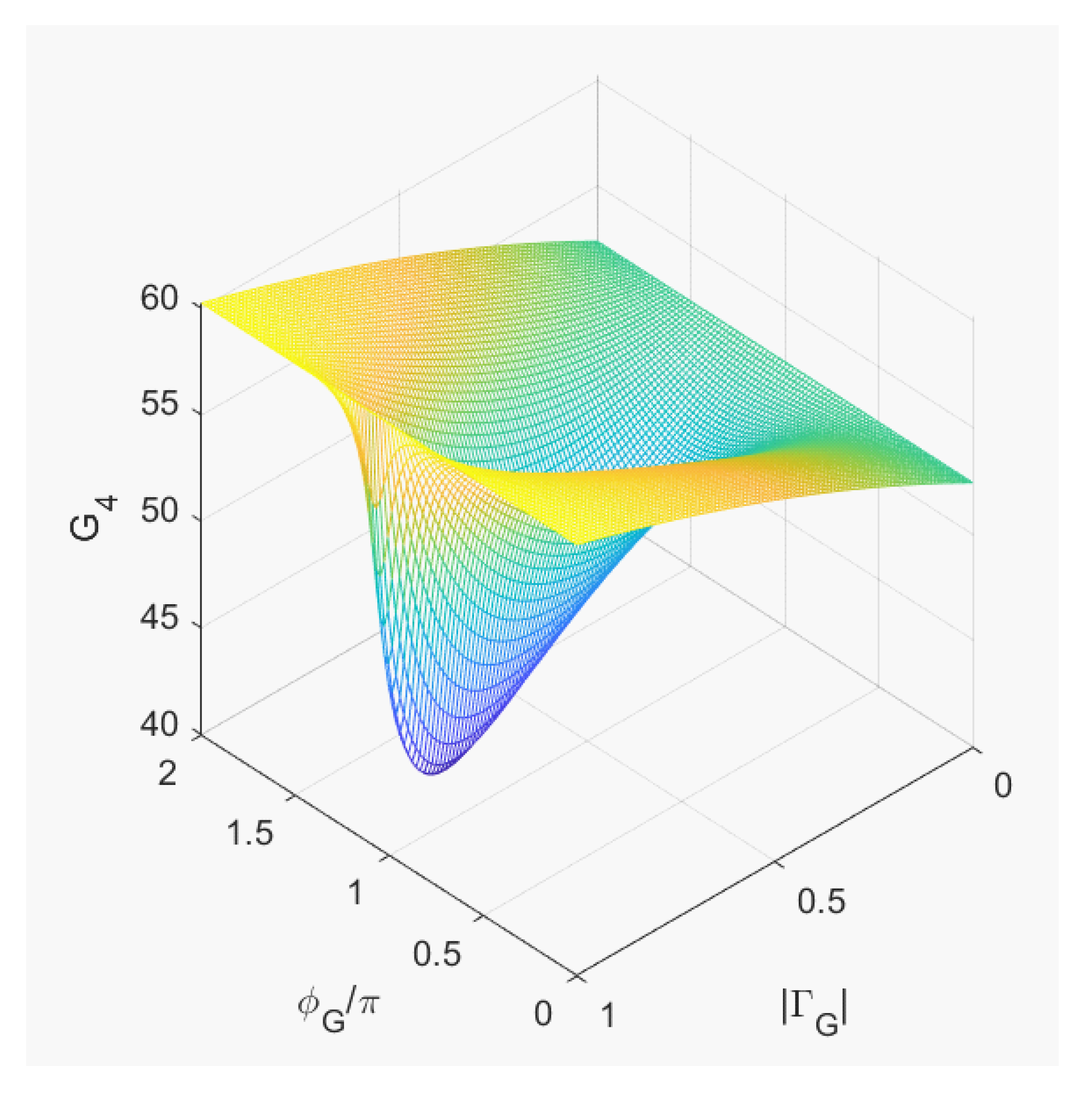
will span between a minimum (generally nonzero) and maximum value, as suggested by the following numerical example. Assume the following constant scattering matrix:
The stability parameters are
and
; the two-port is therefore unconditionally stable with optimum load and source reflectances:
and maximum available gain MAG
. As a first example, we set
and scan the
plane (considering passive loads only), then we plot the surface
where
is the phase of
. The result is shown in
Figure 3;
clearly exhibits a unique minimum in the
plane corresponding to the MAG. Dually, we set
and scan the
plane (considering passive loads only), then we plot the surface
where
is the phase of
. The result is shown in
Figure 4; again, a unique minimum exists in correspondence with
.
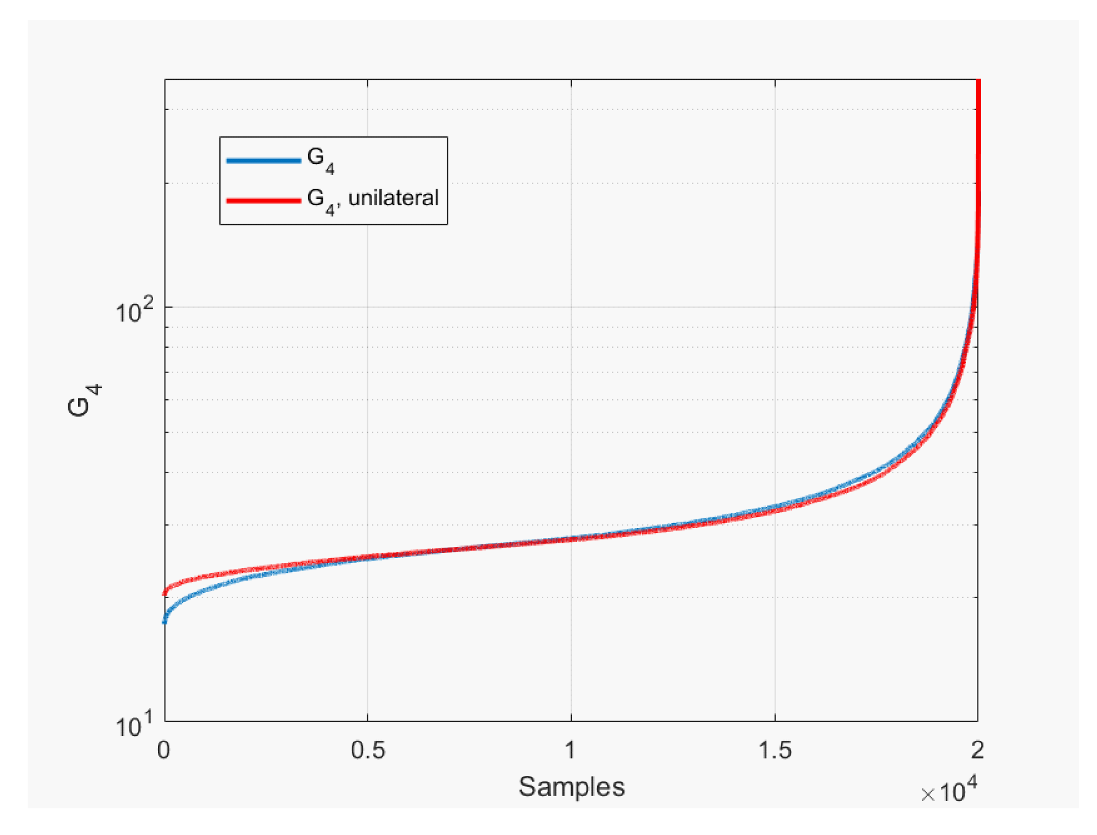
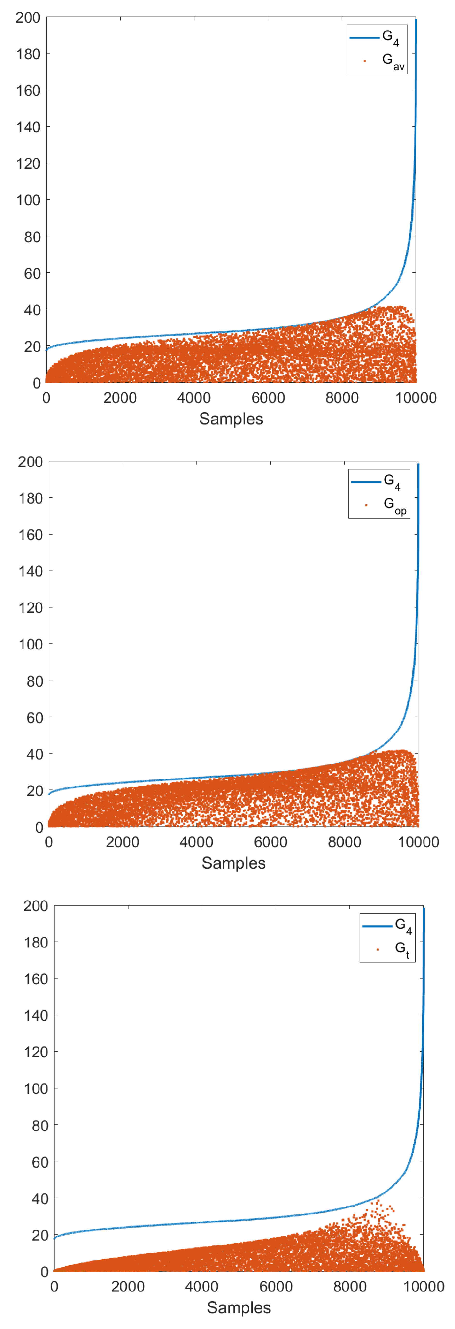
Exploring the behavior of
in the
four-dimensional space is more complex. To provide some hint, we perform a random sampling of the
space, sort the
samples in increasing order, and generate a plot of
vs. the sample order together with a scatter plot of the corresponding values of
,
,
. The
plot together with the unilateral approximation in (
8) is shown in
Figure 5. The minimum and maximum
samples depend of course on the number
N of samples considered; with
N = 100,000, we have
and
.
Finally,
Figure 6 reports a scatter plot of
,
,
(the samples have been ordered with increasing value of
). We remark again that
can be lower or larger than the MAG and that close to the MAG value the samples of
,
, and
exhibit a dense clustering, thus confirming that the condition
MAG does not necessarily correspond to simultaneous conjugate matching. From the scatter plot, it appears that the maximum and minimum of
are associated with load and generator reflectances for which
,
, and
vanish, i.e., with reactive reflectances. A Monte Carlo analysis carried out on
100,000 samples indeed suggests that
is associated with the load and generator impedances with both being reactive, while
is associated with just one reactive termination; however, reactivity alone does not necessarily imply extremum values, since the phase of the reactive termination also has to be properly chosen.
The maximum ratio
can be derived numerically by maximizing the numerator and minimizing the denominator. We have:
where
is the amplitude of the input forward wave generator connected to port 1 of the two-port. This maximum
is obtained for a specific value of the generator reflectance,
, i.e.,:
The input power can be now expressed as:
which is minimum for a certain value of
, i.e.,:
Conversely, the minimum ratio
can be obtained as:
Again, the value of
is obtained for a specific value of the generator reflectance,
, i.e.,:
while
is maximum for a certain value of
, i.e.,:
With the scattering matrix exploited in the example, we have:
and:
confirming that the terminations corresponding to the maximum and minimum of
are reactive. The values obtained by direct search compare well with the previous Monte Carlo analysis.
Finally, it is essential to emphasize the somewhat artificial nature of through a few key points. Let us reconsider the maximum value of and the related maximum available power, , that, as shown in the previous example, occurs by connecting at port 1 a generator with reactive internal impedance. (Notice that while such an ideal generator introduces no anomaly, its available power tends to infinity). The real issue is whether can be actually delivered to a load. The only possible way to do this is by conjugately matching the two-port at the output. But this obviously corresponds to the maximum operational gain MAG (while the available gain and the transducer gain are zero, since the source available power is infinite). Unfortunately, such an output matching is inconsistent with the condition leading to , which implies a reactive load at port 2 and therefore zero power on the load. This ultimately stresses that the input and output loading conditions corresponding to the maximum are totally inconsistent with the purpose of maximum power transfer. This would anyway require conjugate matching at both ports, thus leading to MAG . In conclusion, maximizing does not align with a generator and load condition compatible with maximum power transfer (and similar comments may be made about minimizing ). Nevertheless, understanding the artificial nature of holds, in our opinion, the merit of providing a deeper insight into the fundamental nature of power transfer optimization within a loaded two-port system.


