Abstract
Paralleled buck converters have garnered significant attention for fulfilling the increasing demands of power supplies in modern applications. They have the advantages of increased current capacity and reduced current ripple. Under this architecture, applying distributed control brings the benefits of reliability and scalability. However, the interconnecting lines between the converters are required for achieving the interleaving operation, which reduces the reliability and scalability. To eliminate the interconnecting lines, this paper proposed a hysteresis current controller to achieve the symmetric interleaving operation. First, the parallel structure with a common output filter was proposed to provide the hardware basis for the proposed control method. Then, the hysteresis current controller was constructed based on the inductor voltage of each buck module to achieve the interleaving operation. The experiment of the three-module-paralleled buck converter was conducted. The experimental results show that the symmetric interleaving was achieved with a maximum phase shift error of 4.1%; the output of the parallel system can recover within 2.60 ms after the load transitions from 50% to 100%; and the parallel system can recover within 1.96 ms after one module removal. The simulation results of the six-module-paralleled buck converter show that the parallel system can recover within 1.00 ms after one module addition, which illustrates the scalability of the proposed method.
1. Introduction
The buck converter is one of the most popular topologies for voltage step-down applications [1,2]. The buck converter typically consists of a switching network (a switch and a diode, or two switches) and a filter (an inductor and a capacitor), and the output voltage can be adjusted by the pulse width modulation (PWM). Due to the simple structure, low cost, and high reliability, buck converters have been applied in many applications. For example, servers [3], microgrids [4], and electric vehicles [5] utilize a buck converter as the front-end stage to pre-regulate the voltage to a suitable level [6], and AI engines (Artificial Intelligence Engines) also require buck converters to supply a regulated voltage [7]. However, a single buck converter may struggle to meet high current demands, and thus, several buck modules in parallel are required to share the total current and reduce the total current ripple [7,8,9,10].
The modular structure of paralleled buck converters is well suited for implementing distributed control. In contrast to centralized control, the distributed control disperses the control function into local controllers located within each module. The local controllers cooperate with each other to achieve the coordination and optimization of the paralleled system, and the exit of a module will not affect the operation of the entire system. Therefore, the distributed control methods can enhance the reliability and scalability of the paralleled system [11,12]. Furthermore, the expansion of the parallel converter may bring challenges to stability. However, the stability can be analyzed with an electromagnetic transient simulation platform, e.g., MATLAB Simulink, and frequency-domain stability analysis methods, e.g., impedance-based modeling method [13,14,15]. In addition, the stability can be enhanced according to the results of a simulation or sensitivity analysis to ensure that the system can operate stably after expansion. Therefore, the parallel converters with the distributed control methods have been widely used in microgrids [16,17], traction systems [18,19], etc. However, to achieve the current sharing and total ripple reduction, communications between the modules are required for exchanging the current and phase information. Communications are often achieved by interconnecting lines, which increases the system’s complexity and reduces reliability.
To achieve current sharing without interconnecting lines, a well-established method, i.e., the voltage droop control, is usually utilized [20,21,22]. It adjusts the voltage reference of the module according to its own current, and thus, it does not require information from other modules. However, to reduce the total current ripple, the interconnecting line, which carries the phase information or the synchronous signals, is still required to achieve the interleaving operation. In references [23,24,25], the adjacent modules were connected by the interconnecting lines to transfer the phase angles of the neighboring modules or generate the clock signal, so the local module could generate its carrier to achieve the interleaving operation. Reference [26] reduced the interconnecting lines to a single line. The single signal bus carried the number of modules and sequential number at the same time, enabling the module to generate its control signal with the corresponding phase shift.
However, the interleaving line for ripple reduction still introduces the risk of a single point of failure, reducing the system’s reliability. Therefore, some research has been dedicated to eliminating the interconnecting lines. Reference [27] proposed to use the spike signals on the output voltage to extract the action moment of other modules. Then, the phase-locked loop was used to realize the interleaving operation. It can achieve the interleaving automatically; however, it is noise-sensitive. Reference [28] used the local module current to construct an oscillator circuit for control, so that the system could converge to the interleaving state. However, it required a high sampling rate. References [29,30] constructed a gradient-descent-based controller by sampling the ripple of the module current at a specific time, reducing the requirements for sampling rate. References [31,32] utilized the phase of the module current and voltage to adjust the module phase. Although the interconnecting lines were eliminated, the aforementioned methods are relatively complicated, requiring high-speed analog-to-digital conversion (ADC) and high-performance digital controllers, which distinctly increases the cost.
To achieve the current sharing and current ripple reduction without interconnecting lines, while also ensuring simpler control and lower cost, this paper proposes an analog hysteresis current control method for the paralleled buck converter. The innovations are as follows:
- (1)
- As shown in Figure 1, this paper proposes a modified parallel structure with the common output filter (Lt, Co). The common filter can be implemented by the differential-mode filters, which are required in most of the parallel systems, and thus do not significantly increase the cost. With this structure, the state transition information of other modules can be integrated into the inductor voltage vLi of each module. This configuration provides the hardware basis for the proposed control method.
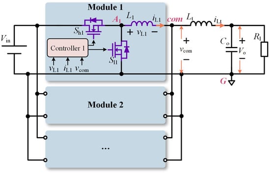 Figure 1. Structure of the paralleled buck converters with the common output filter.
 - (2)
- An analog hysteresis current controller is constructed by utilizing the inductor voltage to generate the hysteresis band. Since the waveform of vLi is correlated with the state transition of other modules, such a hysteresis controller can naturally achieve the interleaving operation, and no interconnecting lines are required.
- (3)
- The proposed hysteresis current controller can achieve the interleaving and the current control simultaneously. Additionally, the cooperation methods of the proposed current controller with the voltage droop control and the voltage outer loop are given.
This paper is organized as follows: Section 2 introduces the proposed structure of the paralleled buck converters. Next, Section 3 describes the proposed hysteresis current controller based on the shaped-inductor-voltage for the interleaving operation, and the simulation results are given. Section 4 gives the implementation methods of the proposed controller. Experimental verifications are given in Section 5. Finally, Section 6 gives the conclusions.
2. The Proposed Structure of the Paralleled Buck Converters
2.1. Structure Specification and Design Considerations
Figure 1 shows the proposed structure of the paralleled buck converters. The main design considerations are as follows:
Each module contains a control switch Shi, a synchronous switch Sli, and an inductor Li, and all of these buck modules are connected together at the point com. Then, the common output filter, consisting of the inductor Lt and the capacitor Co, is connected to power the load Rl. The existence of Lt enables the state transitions of other modules to affect the inductor voltage vLi, which is the hardware basis of the proposed controller to achieve the interleaving operation without interleaving lines. Moreover, the ripple of the total output current iLt flowing through Lt is small, which benefits the magnetic design of Lt.
For each module, a current sensor is used to sample iLi for the inner hysteresis current control. A voltage sensor is used to sample the terminal voltage vcom to realize the outer voltage droop control. In addition, an independent winding is added on Li to sample vLi. Since vLi contains the information of the state transition of other modules, it will be used to construct the hysteresis band for the current control, as well as to achieve the interleaving operation.
It is emphasized that both the current sharing and interleaving operations are achieved by fully utilizing the information of iLi, vcom, and vLi, and thus, no interconnecting lines are required.
2.2. Modeling and Analyses of the Inductor Voltage
For illustration purposes, the following analysis is conducted with the three-module-paralleled buck converter.
The equivalent circuit of the three-module-paralleled system is given in Figure 2a and vAi (i = 1, 2, 3) is the switching node voltage. The switching function for module i (i = 1, 2, 3) is defined as si. When Shi is on and Sli is off, module i is in the on-state, and thus si =1. On the contrary, when Shi is off and Sli is on, module i is in the off-state and thus si = 0. Therefore, vAi can be expressed as
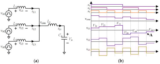
Figure 2.
(a) Equivalent circuit of the paralleled buck converters with common output filter and (b) its voltage waveforms.
Considering that the modules are identical, L1 = L2 = L2 = L is satisfied. According to the superposition theorem, vcom, the voltage of the common point com, can be obtained as
According to Equations (1) and (2), the voltage of inductor L1, L2, and L3 can be calculated as:
From Equations (3)–(5), it can be observed that vLi is related to the input voltage Vin, the output voltage Vo, and the states (the on-state or off-state expressed by the switching function si) of the three modules. Figure 2b gives the voltage waveforms of vL1, vL2, and vL3 when s1, s2, and s3 take different values. Taking vL1 as an example, Equation (6) gives the value of vL1 with different si:
where α = 1/(L + 3Lt), and Σsi = s1 + s2 + s3. For the voltage value Vij with different si, the subscript i represents Σsi (the number of modules that are in the on-state), and the subscript j represents the state of the local module. For example, vL1 = V20 means that two modules in the system are in the on-state and module 1 is in the off-state. Furthermore, Vij satisfies the relation V11 > V21 > V31 > 0 > V00 > V10 > V20.
From (6), several interesting features can be observed. Firstly, vL1 is related to si. Therefore, when si changes, vL1 changes. For example, as point A in Figure 2b, when s1 = 0, s2 = 0, and s3 jump from 1 to 0, vLi jumps synchronously from V10 to V00. This means that vL1 contains the switching states of the other modules, i.e., the phase information. Similarly, the inductor voltages of the other modules exhibit the same characteristics. Therefore, it is possible to utilize vLi to achieve the interleaving operation using appropriate methods.
3. Hysteresis Current Controller Based on Shaped-Inductor-Voltage
Based on the above structure, this paper proposes a hysteresis current controller based on the shaped-inductor-voltage, which utilizes the integrated phase information in vLi to achieve symmetric interleaving without the interleaving line. The subsequent analysis is conducted based on the case of D < 1/3 to illustrate the proposed idea.
3.1. Construction of the Proposed Current Controller
The proposed method is based on the hysteresis current controller. It is one of the classical control methods [33]. Figure 3a shows the waveforms of the traditional hysteresis current controller, which has a fixed hysteresis band with the upper limit hH and the lower limit hL. The voltage viei is the converted current error, which satisfies viei = kiviei = kiv(iLi − Irefi) (kiv denotes the current–voltage ratio, iei denotes the error between the inductor current value iLi and the current reference Irefi). When viei exceeds the preset limit hH or hL, the control signal gi changes to alter the operating state of module i, thereby limiting viei within the hysteresis band. The hysteresis current controller has the advantages of being simple, fast, and stable. However, since the operations of the three modules are independent when this method is directly utilized without communicating the phase information, the frequencies of the three modules are likely to be different, and it is challenging to achieve the interleaving operation.
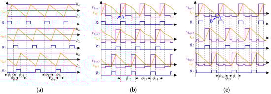
Figure 3.
Construction of the hysteresis current controller. (a) Traditional hysteresis current controller, (b) hysteresis current controller with vLi directly constructing the hysteresis band and (c) the proposed hysteresis current controller based on the shaped-inductor-voltage.
Therefore, the inductor voltage vLi, which contains the phase information, is directly used to construct the hysteresis band, as illustrated in Figure 3b. This hysteresis band produces the correction of the control signals for the modules. For example, as point A shows in Figure 3b, when g2 changes from 1 to 0, vhys1 simultaneously steps upward, causing vie1 to exceed vhys1; hence, g1 jumps to 1. This correction enables the three modules to operate at the same switching frequency without interconnecting lines.
However, the phase angle ϕ12, ϕ23, and ϕ31 between these modules are not the desired value (i.e., ϕ12 = ϕ23 = ϕ31 = 120°). This is because the voltage step resulting from the state transition of other modules causes an immediate step in the hysteresis band, which may immediately change the module state. To fix this problem, the voltage jump (as shown in point B in Figure 3c) is modified as a ramp (as shown in region C in Figure 3c). This modification delays the switching moment. (As shown in region C. After g3 jumps to 0, vhys1 does not follow the inductor voltage, instead, it gradually attenuates until it equals vie1, and subsequently, g1 jumps to 1). Based on the designs above, a hysteresis current controller based on the shaped-inductor-voltage is proposed in this paper. The proposed hysteresis current controller can automatically converge to the symmetric interleaving operation state. The detailed analysis is given as follows.
3.2. Analysis of Interleaving Operation
The steady state waveforms of the proposed controller are given on the left of Figure 4 (see the “steady state” region). The errors of the waveform transformation process and the delay and error of the current sampling are neglected in the analysis. The upper and lower limits of the hysteresis band vhysi can be expressed as
where i = 1~3, and ki is the voltage adjustment coefficients of module i, which are constant and determined by the hardware. Since the modules are the same, k1 = k2 = k3 = k, and hmin1 = hmin2 = hmin3 = hmin, hmax1 = hmax2 = hmax3 = hmax are satisfied.
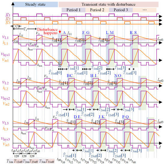
Figure 4.
Key waveforms of the steady state and the transient state for D < 1/3.
According to the waveforms of the inductor current and the hysteresis band, the minimum and maximum inductor currents in the steady state satisfy the following relationships:
where Ii0 and Ii1 are the minimum and maximum current of module i, respectively; Irefi is the current reference of module i; a00, a10, and a11 are the current changing rates, and a00 = V00/L, a10 = V10/L; and a11 = V11/L are satisfied. λi is the attenuation rate of the ramp in vhysi. λi and kiv are determined by the hardware design and considering that the parameters of the three modules are the same, λ1 = λ2 = λ3 = λ are satisfied. T1on, T2on, and T3on are the periods when module 1, module 2, and module 3 are in the on-state, respectively. T12off, T23off, T31off are the periods of ts1~ts2, ts3~ts4, ts5~ts6, respectively, as shown in Figure 4.
Considering a small disturbance happens during t00~t11 on module 1, which breaks the steady state, Irefi is assumed to be constant and equal to its steady-state value during this process. Since Irefi is generated by the voltage outer loop with a relatively slow response speed compared to the current inner loop, this assumption is reasonable. The small disturbance causes a deviation of ΔT31off[0] from the steady-state value T31off, and the length of this time interval 31off[0] is
With the analysis in Appendix A, the expressions of ΔT31off[k] can be derived as
where the coefficient α is
where λiv satisfies λiv = λ/kiv.
The coefficients are relatively complex. Therefore, to demonstrate that the system can return to the steady state under the disturbance, the hardware parameters in Table A1 are substituted into Equations (16)–(18). Figure 5 shows the variation curve of ΔT31off[k]/ΔT31off[0] with respect to the number of recurrences. It can be seen that ΔT31off[k]/ΔT31off[0] reduces rapidly when k ≥ 2, ΔT31off[k]/ΔT31off[0] ≈ 0 holds when the recurrence number k ≥ 17. This demonstrates that ΔT31off[k] gradually approaches zero after several periods, i.e., 31off[k] can converge to the corresponding steady-state value T31off. Similarly, the deviations of other intervals can also converge to zero. Therefore, the system can recover to a steady state after the small disturbance, which indicates that the proposed controller exhibits good stability. Figure A1 in Appendix A gives more numerical results with different Vin, Vo, or λ. The curves show that ΔT31off[k] can also gradually approach zero under these conditions. This further validates that the proposed controller can recover to the steady state.
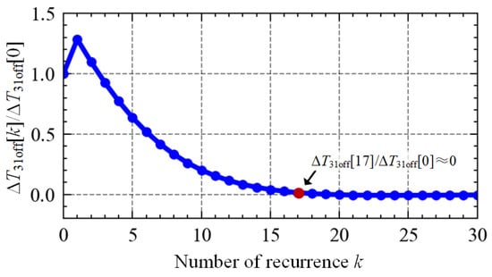
Figure 5.
Variation curve of ΔT31off[k]/ΔT31off[0].
When the modules are working under the steady state, the three modules in the system have the same period Ts (frequency), i.e., Ts = T1on + T2on + T3on + T12off + T23off + T31off. Therefore, according to the volt-second balance principle, these modules satisfy
The difference between (20) and (21) yields (V10 − V01)(T1on − T2on) = 0. Since V10 > 0 > V01 holds, it is established that V10 − V01 > 0 consistently holds. Therefore, T1on = T2on can be derived. With the similar method, it can be derived that
which indicates that the duty cycles of the three modules in the system are the same for the steady state.
This represents that the three modules have the same duty cycle D in the steady state. With (23), the difference between (9) and (10) yields T12off = T31off. With similar method, the following expression holds
Therefore, based on Equations (23) and (24), it can be derived that
in other words, the phase angles between the three modules satisfy the relationship of ϕ12 = ϕ23 = ϕ31 = 120°. The above analyses prove that with the proposed hysteresis current controller, the three modules can realize the symmetric interleaving in the steady state.
The steady-state waveforms for the cases of 1/3 ≤ D ≤ 2/3 and D ≥ 2/3 are shown in Figure 6. Although the position of the ramp in vhysi is slightly different, it can also demonstrate that the symmetric interleaving operation can be achieved using a similar analysis method.
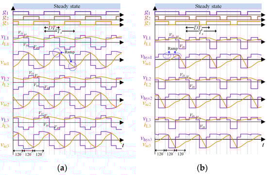
Figure 6.
Steady-state waveforms for the case of (a) 1/3 ≤ D ≤ 2/3 and (b) D > 2/3.
Although the above analysis is based on the three-module-paralleled system, the proposed method can be utilized in the system with two or more modules, and the analysis methods above and the conclusions still hold.
3.3. Simulation Verification
To validate the above analysis, the paralleled buck converters are built in MATLAB Simulink with the parameters in Table A1.
Figure 7a depicts the dynamic process with the disturbance of the current reference Iref, with Vin = 48 V. During the simulation, Iref1 = Iref2 = Iref3 = Iref are given, and Iref is set to change from 1.8A to 0.9A. Before the disturbance, the three modules achieve the symmetric interleaving operation with phase angles of 120°, as shown in Figure 7b. When the disturbance occurs, the phase angles are affected but the system can gradually converge to the steady state with the phase angle of 120°, as shown in Figure 7c. This verifies that the three-module-paralleled system can automatically adjust the phase after disturbance and can converge to the symmetric interleaving state. Furthermore, Figure 7d shows the key waveforms of the proposed hysteresis current controller in module 1, with Iref = 1.8A. A hysteresis delay of 0.05 V for realizing the comparison of vie1 and vhys1 is used to enhance the anti-interference capability. The waveforms well match the analysis waveforms in Figure 4. It can be observed that several voltage jumps exist on vL1, which are introduced by the actions of other modules in the system, and these voltage jumps are adjusted to the voltage ramps on vhys1, e.g., region A in Figure 7d.
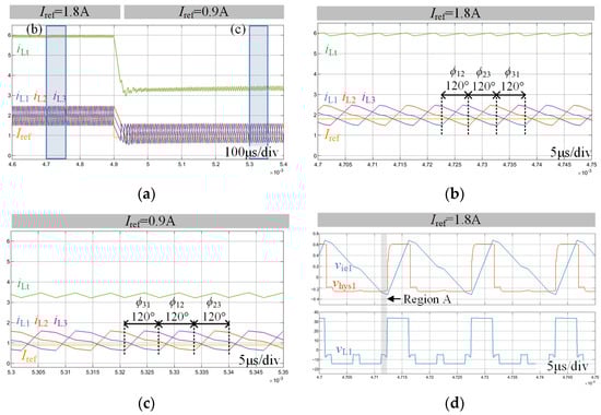
Figure 7.
Simulation results of (a) the dynamic process with the disturbance of Iref, (b,c) the zoomed views of the steady states and (d) the key waveforms of the proposed hysteresis current controller.
Figure 8a,b give the simulation results of the steady state waveforms for 1/3 ≤ D ≤ 2/3 (with Vin = 24 V and Iref = 2A) and D > 2/3 (with Vin = 16 V and Iref = 2A), respectively. The waveforms also match those in Figure 6 and the symmetric interleaving can also be achieved in both cases.
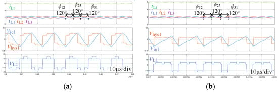
Figure 8.
Steady-state waveforms for (a) 1/3 ≤ D ≤ 2/3 and (b) D > 2/3.
Figure 9a gives the simulation results of a six-module-paralleled system and it shows that the system can restore stability after module addition. The zoomed views in Figure 9b,c show that both the five-module-paralleled system and the six-module-paralleled system can operate in the symmetric interleaving states, with phase angles of 72° (360°/5) and 60° (360°/5), respectively. The proposed method is effective for the system with more modules. In addition, it has hot-plug capability and the phase angles can automatically adjust.
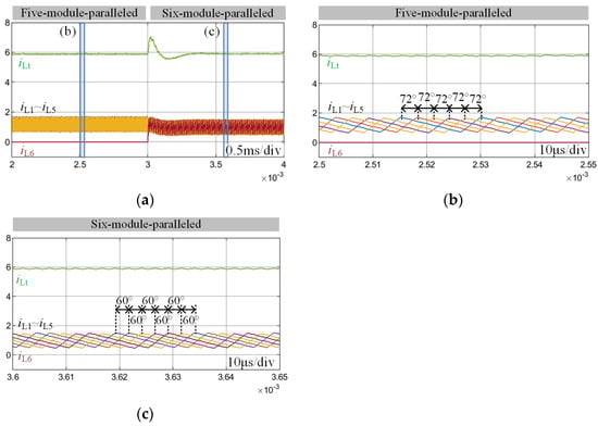
Figure 9.
Simulation results of the module addition. (a) The dynamic process and the zoomed views of the stable state of (b) the five-module-paralleled system and (c) the six-module-paralleled system.
4. Implementation of the Proposed Hysteresis Current Controller
4.1. Hardware Design of the Proposed Hysteresis Current Controller
The proposed hysteresis current controller is implemented by analog methods.
According to the analysis above, the proposed hysteresis current controller has integrated the phase information into the waveform of vLi to eliminate the interconnecting lines. However, the actions of the switches result in high-frequency noise on vLi, and the noise increases with the increase in the operating voltage and current. Therefore, when implementing the proposed hysteresis current controller, it is necessary to use some methods, such as isolated sampling and filtering, to cope with the noise and to guarantee the stability of control.
Figure 10 shows the circuit diagram of the controller in module i. An independent winding of W turns is added to the inductor to sample vLi and the isolated sampling method ensures strong noise immunity. The sampled signal vseci is proportional to vLi and is used to construct the hysteresis band vhysi. Furthermore, the low-pass filter with a bandwidth of 1.06 MHz is employed to filter out the high-frequency noise while not affecting the voltage jump information (i.e., phase information) in vseci. To generate the ramp, the positive part and negative part of the waveforms of vseci are separately shaped.
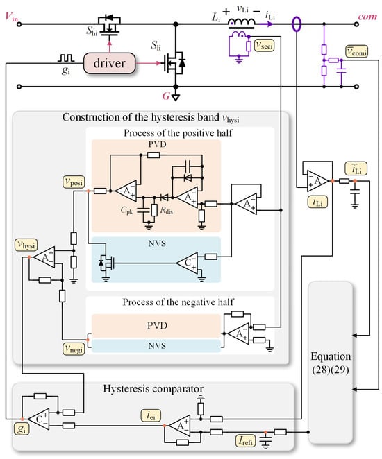
Figure 10.
The circuit diagram of module i.
For the positive part shaping, a peak voltage detection (PVD) circuit is utilized to detect and maintain the maximum value. The discharging resistor Rdis is paralleled across the capacitor Cpk of the PVD circuit to form the required ramp. When vseci falls, Cpk discharges through Rdis, converting the voltage jump into the slowly discharging voltage. Moreover, during the period when vseci is less than zero, the output of the PVD circuit is clamped to 0 by the negative voltage shielding (NVS) circuit, avoiding its influence on the shaping of the negative part. Thereout, the shaped voltage vposi for the positive part is obtained. The values of Cpk and Rdis need to be chosen carefully. Cpk should not be too large so that the PVD circuit can track the peak value quickly, while Rdis needs to be carefully chosen to ensure that the ramp always exists before the next state transition of this module. Furthermore, the low-pass filter is added to each stage of the operational amplifier to avoid noise interference.
For the negative part shaping, vseci is firstly inverted by the phase inverter, and then vnegi can be obtained using the same method of processing vposi. Subsequently, vposi and vnegi are combined by the subtractor to obtain vhysi. Both vhysi and the current error iei of module i are fed into the hysteresis comparator to generate the control signal gi for module i. The hysteresis comparator can suppress noise and enhance the stability of the comparison.
From the implementation process of the proposed hysteresis current controller, it can be seen that to construct vhysi with vLi, the analog basis method is the most convenient and cost-efficient way (in the digital method, the high-speed ADC and digital controller are required to realize hysteresis operation, leading to an increase in implementation costs). Furthermore, due to the simple structure of the proposed hysteresis control, only the voltage adjustment coefficients ki (voltage divider resistors) and attenuation rate λ (Cpk and Rdis) need to be tuned.
4.2. Cooperation with the Voltage Outer Loop and the Voltage Droop Control
Furthermore, the proposed current hysteresis controller can achieve both the interleaving and the inner loop current control. The required current reference Irefi comes from the voltage droop control for current sharing and the voltage outer loop, which can be implemented with common methods.
To realize the voltage outer loop, the output voltage Vo is rebuilt from the terminal voltage vcomi of each module. vcomi of module i can be expressed with
where vLt is the transient voltage across the common inductor Lt, and vo is the transient output voltage. Filtering the signal vcomi with a simple RC filter, the low-frequency components of vcomi, namely comi, can be obtained (the time constant of the RC filter should be much smaller than that of the outer voltage loop). Mathematically, comi is
In (27), the average inductor voltage Lt converges to zero due to the volt-second balance principle; therefore, comi is dominated by the filtered average voltage o, i.e., Vo. Therefore, comi can be used to estimate Vo as the feedback in the outer voltage loop. The expression of the voltage outer loop based on the PI (Proportional-Integral) controller can be expressed as
where Kp and Ki are the proportional and integral coefficients, respectively. Moreover, Vrefi_dr is the voltage reference with a droop feature. The output of the controller is treated as the current reference Irefi of the inner hysteresis controller.
For voltage droop purpose, Vrefi_dr is obtained by introducing the average of the sampled current value Li as feedback
where kdr represents the droop coefficient and Vref represents the voltage reference value. With (29), the goal of the voltage droop is to achieve the balance of Li. Since Li equals the output current Ioi, the output currents can also be naturally shared.
5. Experimental Verification and Discussion
To experimentally validate the proposed hysteresis current controller, a three-module system prototype was built with the parameters in Table A1, as shown in Figure 11. It can be seen that there are only power connections among the modules, and no interconnection lines exist for signal transmission.
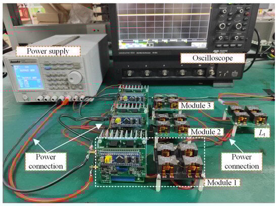
Figure 11.
Prototype of the three-module-paralleled buck converter.
Figure 12a,b show the dynamic processes of the load transitions while maintaining Vo at 12 V. It can be seen that the paralleled system can achieve the regulation of Vo. After the load addition in Figure 12a, the steady-state value of Vo decreased from the original value of 11.99 V to 11.85 V due to the voltage droop control, and after the load removal in Figure 12b, Vo recovered from 11.85 V to 11.99 V. Meanwhile, the inductor currents of the three modules, iL1, iL2, and iL3, are always overlapped, which indicates that the current sharing can be achieved even in the dynamic processes. The current sharing error is within 4.0%.
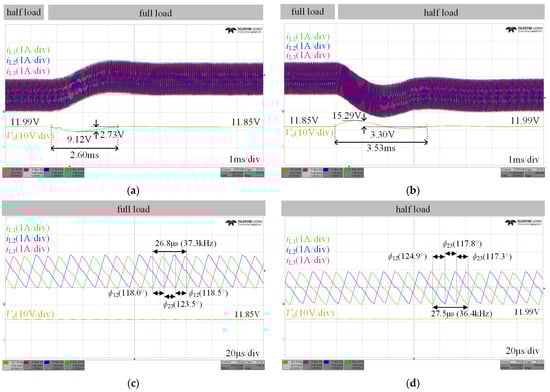
Figure 12.
Measured waveforms of the dynamic process of (a) the load addition and (b) the load removal, and the zoomed views of the steady states of (c) full load and (d) half load.
The interleaving operation can be further observed in Figure 12c,d. Figure 12c shows the zoomed view of the steady state with the full load, and the phase angles ϕ12, ϕ23, and ϕ31 were 118.0°, 123.5°, and 118.5°, respectively. Figure 12d shows the zoomed view of the steady state with the half load, and the phase angles ϕ12, ϕ23, and ϕ31 were 124.9°, 117.8°, and 117.3°, respectively. The phase angles of both states were close to the desired value of the symmetric interleaving 120° (360°/3), with a maximum relative error of 4.1%. This demonstrates that the proposed method can automatically achieve the symmetric interleaving operation.
From the experimental results above, it can be seen that for the proposed method, the phase shift error and the current sharing error exist. The phase shift error results from the inconsistencies of the hardware parameters, including the delay of the comparator, and the accuracy of the resistors. These inconsistencies are inherent problems of using the analog circuits for generating the control signals. For the methods with interconnecting lines, the information on the lines is always generated by the digital controllers. Therefore, the phase shift error and the current sharing error result from the accuracy of the phase lock loop (PLL) and the ADC. For example, [26] utilizes one interconnecting line to carry a synthetic signal generated by the operating modules. With the synthetic signal, each module can decode the total number of operating modules and its sequential number, thereby achieving the interleaving and current sharing. The phase shift error results from the PLL, e.g., the phase shift error of the method in [26] is about 5.4%. Furthermore, the error of the proposed method can be further decreased by selecting the resistors with higher precision and analog devices with more consistent characteristics or integrating the circuits by using integrated circuit technology to improve the consistency.
Figure 13 gives the waveforms of two extreme situations, i.e., the module removal and addition. Figure 13a gives the waveforms of the dynamic process when removing module 3 from the three-module-paralleled system. After the removal of module 3, Vo stabilized at 11.77 V after 1.96 ms. Furthermore, iL1 and iL2 increased simultaneously and maintained the current sharing throughout the dynamic process. Figure 13b gives the zoomed view of the module removal. It can be observed that when module 3 was removed, the phase angles of the remaining modules automatically adjusted and gradually approached the values under the symmetric interleaving state. The zoomed view of the steady state is given in Figure 13c and it shows that the two remaining modules could also achieve the symmetric interleaving operation with the phase angles of 177.9° and 182.1°, which are close to 180° (360°/2) with a relative error of 1.2%.
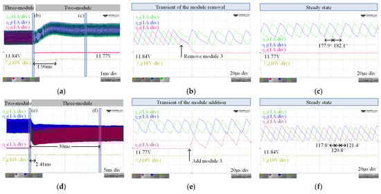
Figure 13.
Dynamic processes of (a) the module removal and its zoomed views (b,c), and (d) the module addition and its zoomed views (e,f).
Figure 13d gives the dynamic waveforms of the module addition. The addition of module 3 to a two-module-paralleled system resulted in the fluctuations of Vo; nevertheless, Vo could stabilize at 11.84 V with a settling time of 2.41 ms. As iL3 increased, iL1 and iL2 decreased, and the current sharing among the three modules was achieved after about 30 ms. The transient of module addition is shown in Figure 13e, and it shows that when module 3 was added, the phase angles adjusted automatically. Figure 13f shows the zoomed view of the steady state, where the two-module-paralleled system could also achieve the symmetric interleaving operation with the maximum relative error of 1.2%.
The above experimental results demonstrate that the proposed hysteresis current controller has the hot-plug capability, which enhances the modularity, scalability and redundancy of the system.
Most of the hot-plug methods are achieved based on digital controllers. Therefore, these methods require detection of the circuit state to determine whether the module is added or removed. Then, the controller can adjust the phase shift cycle by cycle based on the detection results, and the system recovers to a stable state after multiple periods. On the contrary, the proposed method uses the analog hysteresis current controller to achieve both the current sharing and the interleaving. Consequently, once the module is added or removed, the waveform of vLi is immediately changed, resulting in the synchronous changes in the hysteresis band vhysi. Furthermore, the inductor current can quickly respond to the change in vhysi. Therefore, the dynamic processes can be faster.
To compare the hot-plug performance, the simulation of the proposed method under similar conditions of the method in [31] (It is realized with digital controllers without the interleaving lines) was conducted. The parameters are given in Table A2 and the results are given in Figure 14. It can be seen that after the module addition, Vo recovered to the stable value after 731 μs. Additionally, the symmetric interleaving and current sharing were achieved after 348 μs and 3 ms, respectively. In contrast, for the method in [31], the dynamic process lasted for 13 ms. In addition, for the module removal process, the current sharing is always achieved. Vo recovered to the stable value after 447 μs and the symmetric interleaving was achieved after 316 μs. These times are much shorter than those of the method in [31] (13 ms). Therefore, the dynamic processes of both the module addition and removal are much faster than the method in [31].
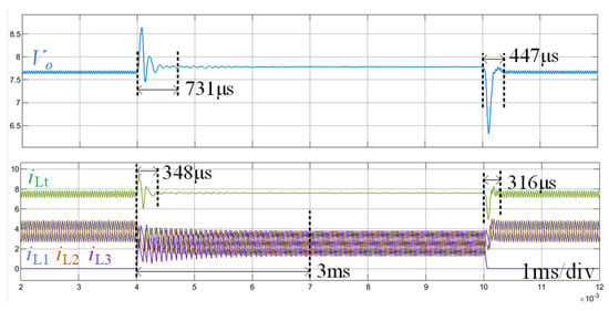
Figure 14.
Simulation of the dynamic processes of module addition and removal.
6. Conclusions
This paper proposes a hysteresis current controller for the paralleled buck converters to achieve the interleaving operation without the need for interconnecting lines. Firstly, the paralleled structure is slightly modified to integrate the phase information into the inductor voltage in the module. Then, the hysteresis current controller based on the shaped-inductor-voltage is designed and with the controller, the symmetric interleaving is automatically achieved. The effectiveness of the proposed control method is validated through simulations and experiments. The results confirm the following:
- (1)
- The proposed hysteresis control can achieve symmetric interleaving of the modules, with the maximum phase angle error of 4.1%;
- (2)
- The current sharing can be achieved by combining the proposed controller with the voltage drop control, and the error of current sharing is within 4.0%;
- (3)
- The hot-plug capability is verified. The modules can achieve the current sharing after adding the new module for 30 ms and can keep the current sharing after removing one module. At the same time, the phase angles can automatically adjust to the symmetrical interleaving state.
- (4)
- The output voltage can recover within 2.60 ms after the load transitions from 50% to 100% and recover within 3.53 ms after the load transitions from 100% to 50%. In addition, the output voltage can recover within 1.96 ms after one module removal and recover within 2.41 ms after one module addition.
The proposed method utilizes an additional winding to sample the inductor voltage for constructing the hysteresis band, thereby eliminating the need for isolated voltage sensors. Furthermore, the construction of the hysteresis band and the generation of the control signals are implemented by analog circuits, thereby eliminating the need for high-speed ADC and a high-performance digital controller. These characteristics demonstrate that the proposed method has the merits of low cost and simplicity. Additionally, the results of the load transitions and hot-plug demonstrate the robustness. Therefore, the proposed controller can reliably achieve the desired control objectives without the need for interconnecting lines, making it highly potential for those applications that require reliability, modularity, and scalability.
The proposed method is hysteresis-control-based, which suffers from frequency variation with voltage variation. Hence, one of the future research opportunities will be to reduce the frequency variation range of the proposed control to facilitate the filter design. In addition, future research will extend this method to other paralleled DC–DC converters. Moreover, the proposed idea is currently verified by the circuit with discrete components, however, such a circuit is suitable for being made into integrated chips so as to further reduce costs and improve reliability and consistency.
Author Contributions
Conceptualization, R.W. and Y.C.; methodology, R.W. and Y.C.; software, R.W.; validation, R.W., J.H. and Y.W.; formal analysis, R.W.; investigation, R.W., J.H. and Y.W.; resources, R.W. and Y.C.; data curation, R.W.; writing—original draft preparation, R.W. and Y.C.; writing—review and editing, R.W., Y.C. and J.H.; visualization, R.W.; supervision, Y.C. and Y.K.; project administration, Y.C. and Y.K.; funding acquisition, Y.C. All authors have read and agreed to the published version of the manuscript.
Funding
This research was funded by the Young Top-notch Talent Cultivation Program of Hubei Province.
Data Availability Statement
Data are contained within the article.
Conflicts of Interest
The authors declare no conflicts of interest.
Appendix A
- Derivation of Equations (16)–(18)
With the voltage-current relationship of the inductor, the resulting current disturbance 10[1] is
Combining Equation (9), the current deviation ΔI10[1] can be solved as
(1) [t10~t11]: As range A in Figure 4 shows, for module 1, iL1 increases to the maximum current I11, and I11 is determined by hmax1 which is not affected by the disturbance. I11 can be expressed as
where 1on[1] is the length of this time interval, and 1on[1] = T1on + ΔT1on[1] is satisfied. Combining Equations (12) and (A2), ΔT1on[1] can be solved as
(2) [t11~t12]: As range B in Figure 4 shows, for module 2, iL2 decreases to the minimum current 20[1] and it can be expressed as
where 12off[1] is the length of this time interval. Therefore, combining Equation (10), ΔT21off[1] and the current deviation ΔI20[1] can be solved as
where the coefficient λiv satisfies λiv = λ/kiv.
(3) [t12~t13]: As range C shows, for module 2, iL2 increases to the constant maximum current. I21 can be expressed as
where 2on[1] is the length of this time interval. According to Equation (13), the time deviation from T2on is
(4) [t13~t14]: As range D shows, for module 3, iL3 decreases to the minimum current 30[1], and it can be calculated as
where 23off[1] is the length of this time interval. 23off[1] and the current deviation ΔI30[1] can be solved combining Equation (11):
(5) [t14~t15]: As range E shows, for module 3, the maximum current I31 is
where 3on[1] is the length of this interval. Combining Equation (14), the deviation from T3on can be solved as
(6) [t15~t20]: As range F shows, for module 1, similar to the analysis of range D, the deviation ΔT31off[1] from the steady-state value T31off is
Substituting Equations (A9) and (A14), Equation (A15) can be modified as:
Hence, the relationship between ΔT31off[1] and ΔT31off[0], i.e., Equation (16), can be obtained by substituting Equations (A4), (A6), (A9) and (A11).
Additionally, the current deviation ΔI10[1] is
(7) [t20~t21]: As range G shows, for module 1, similar to the analysis of range E, the deviation ΔT1on[2] has a similar form of Equation (A14), that is,
(8) Then, sequentially analyze range H~R in Figure 4 with the same method. The recurrence equations between different intervals can be derived as
Based on the above equations, when k = 2, ΔT31off[2] can be calculated. In addition, combining Equations (16), (A4), (A6), (A9), (A11), and (A16)–(A18), the relationship between ΔT31off[2], ΔT31off[1] and ΔT31off[0], i.e., Equation (17), can be obtained.
Additionally, when k > 2, substituting ΔT12off[k] and ΔT23off[k] into ΔT31off[k], Equation (A21) is
Subsequently, substituting ΔT23off[k−1] and ΔT12off[k] yields
According to Equation (A21), when k > 2, (ΔT12off[k−1] + ΔT23off[k−1]) = ΔT31off[k−1]/α is satisfied; therefore, Equation (18) can be obtained by substituting this relationship into Equation (A23).
- 2.
- Variation curves of ΔT31off[k]/ΔT31off[0]
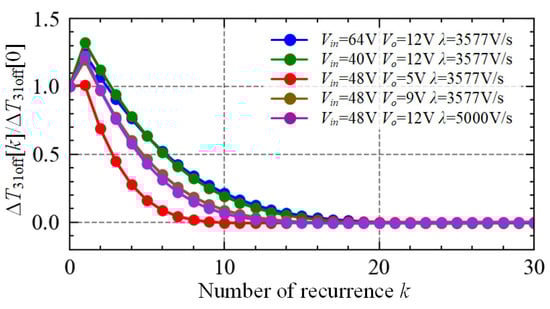
Figure A1.
Variation curves of ΔT31off[k]/ΔT31off[0] with different parameters.
- 3.
- Parameters

Table A1.
Parameters for the simulations and experiments.
Table A1.
Parameters for the simulations and experiments.
| Parameter | Value |
|---|---|
| Inductor inside the module Li | 132 μH |
| Common inductor Lt | 60 μH |
| Common capacitor Co | 250 μF |
| Rated input voltage Vin | 48 V |
| Output voltage Vo | 12 V |
| Rated load Rl | 2 Ω |
| Voltage adjustment coefficients ki | 0.018 V/V |
| Attenuation rate λ | 3577 V/s |
| Current–voltage ratio kiv | 1.0 V/A |
Table A2.
Parameters for the simulations of Figure 14.
Table A2.
Parameters for the simulations of Figure 14.
| Parameter | Value |
|---|---|
| Inductor inside the module Li | 180 μH |
| Common inductor Lt | 60 μH |
| Common capacitor Co | 50 μH |
| Rated input voltage Vin | 24 V |
| Output voltage Vo | 8 V |
| Rated load Rl | 1 Ω |
| Voltage adjustment coefficients ki | 0.1 V/V |
| Attenuation rate λ | 20,000 V/s |
| Current–voltage ratio kiv | 1.0 V/A |
References
- Shenoy, P.S.; Amaro, M.; Morroni, J.; Freeman, D. Comparison of a Buck Converter and a Series Capacitor Buck Converter for High-Frequency, High-Conversion-Ratio Voltage Regulators. IEEE Trans. Power Electron. 2016, 31, 7006–7015. [Google Scholar] [CrossRef]
- Kim, D.; Hong, M.; Baek, J.; Lee, J.; Shin, J.; Shin, J.W. Soft-Switching Auxiliary Current Control for Improving Load Transient Response of Buck Converter. IEEE Trans. Power Electron. 2021, 36, 2488–2494. [Google Scholar] [CrossRef]
- Mandru, N.; Nithyadas, P.; Kundu, U.; John, V. Bootstrap Operation in eGaN-Based Full-Wave ZCS Quasi-Resonant Synchronous Buck Converter for Server Application. In Proceedings of the 2023 IEEE Applied Power Electronics Conference and Exposition (APEC), IEEE, Orlando, FL, USA, 19–23 March 2023; Volume 2023, pp. 2239–2244. [Google Scholar]
- Hassan, M.A.; Li, E.P.; Li, X.; Li, T.; Duan, C.; Chi, S. Adaptive Passivity-Based Control of DC-DC Buck Power Converter with Constant Power Load in DC Microgrid Systems. IEEE J. Emerg. Sel. Top. Power Electron. 2019, 7, 2029–2040. [Google Scholar] [CrossRef]
- Besharati Rad, A.; Kargaran, M.; Meghdadi, M.; Medi, A. A Wide-Input-/Output-Voltage-Range Buck Converter with Adaptive Light-Load Efficiency Improvement and Seamless Mode Transition. IEEE Trans. Power Electron. 2024, 39, 2200–2212. [Google Scholar] [CrossRef]
- Reusch, D.; Biswas, S.; Zhang, Y. System Optimization of a High Power Density Non-Isolated Intermediate Bus Converter for 48 v Server Applications. IEEE Trans. Ind. Appl. 2019, 55, 1619–1627. [Google Scholar] [CrossRef]
- Liu, W.C.; Cheng, C.H.; Mi, C.; Mercier, P. A Novel Ultrafast Transient Constant On-Time Buck Converter for Multiphase Operation. IEEE Trans. Power Electron. 2021, 36, 13096–13106. [Google Scholar] [CrossRef]
- Su, J.-T.; Liu, C.-W. A Novel Phase-Shedding Control Scheme for Improved Light Load Efficiency of Multiphase Interleaved DC–DC Converters. IEEE Trans. Power Electron. 2013, 28, 4742–4752. [Google Scholar] [CrossRef]
- Perreault, D.J.; Kassakian, J.G. Distributed Interleaving of Paralleled Power Converters. IEEE Trans. Circuits Syst. I 1997, 44, 728–734. [Google Scholar] [CrossRef]
- Roh, Y.S.; Moon, Y.J.; Park, J.; Jeong, M.G.; Yoo, C. A Multiphase Synchronous Buck Converter with a Fully Integrated Current Balancing Scheme. IEEE Trans. Power Electron. 2015, 30, 5159–5169. [Google Scholar] [CrossRef]
- Sadabadi, M.S.; Mijatovic, N.; Tregouet, J.-F.; Dragicevic, T. Distributed Control of Parallel DC–DC Converters Under FDI Attacks on Actuators. IEEE Trans. Ind. Electron. 2022, 69, 10478–10488. [Google Scholar] [CrossRef]
- Wenkang, H.; Schuellein, G.; Clavette, D. A Scalable Multiphase Buck Converter with Average Current Share Bus. In Proceedings of the Eighteenth Annual IEEE Applied Power Electronics Conference and Exposition, 2003. APEC ’03., IEEE, Miami Beach, FL, USA, 9–13 February 2003; Volume 1, pp. 438–443. [Google Scholar]
- Wang, H.; Liu, J.; Hou, D. Derivation Method of Output Impedance of DC-DC Converters Paralleled System with Active Current Sharing Control for System Stability Analysis. In Proceedings of the 2010 International Power Electronics Conference—ECCE ASIA, Sapporo, Japan, 21–24 June 2010; pp. 213–217. [Google Scholar]
- Meng, X.; Zhang, Q.; Liu, Z.; Hu, G.; Liu, F.; Zhang, G. Multiple Vehicles and Traction Network Interaction System Stability Analysis and Oscillation Responsibility Identification. IEEE Trans. Power Electron. 2024, 39, 6148–6162. [Google Scholar] [CrossRef]
- Alenius, H.; Berg, M.; Luhtala, R.; Roinila, T.; Messo, T. Impedance-Based Stability Analysis of Multi-Parallel Inverters Applying Total Source Admittance. In Proceedings of the 2019 20th Workshop on Control and Modeling for Power Electronics (COMPEL), Toronto, ON, Canada, 17–20 June 2019; pp. 1–8. [Google Scholar]
- Nasirian, V.; Moayedi, S.; Davoudi, A.; Lewis, F.L. Distributed Cooperative Control of DC Microgrids. IEEE Trans. Power Electron. 2015, 30, 2288–2303. [Google Scholar] [CrossRef]
- Pulvirenti, F.; La Scala, A.; Ragonese, D.; D’Souza, K.; Tina, G.M.; Pennisi, S. 4-Phase Interleaved Boost Converter With IC Controller for Distributed Photovoltaic Systems. IEEE Trans. Circuits Syst. I 2013, 60, 3090–3102. [Google Scholar] [CrossRef]
- Meng, X.; Hu, G.; Liu, Z.; Wang, H.; Zhang, G.; Lin, H.; Sadabadi, M.S. Neural Network-Based Impedance Identification and Stability Analysis for Double-Sided Feeding Railway Systems. In IEEE Transactions on Transportation Electrification; IEEE: Piscataway, NJ, USA, 2024; p. 1. [Google Scholar] [CrossRef]
- Lin, C.; Ge, X.; Wang, H.; Meng, X.; Mu, J.; Liu, Z. Low-Frequency Stability Analysis of Train-Grid System: A Perspective From DAB Converter. IEEE Trans. Power Electron. 2024, 39, 9066–9071. [Google Scholar] [CrossRef]
- Kim, J.W.; Choi, H.S.; Cho, B.H. A Novel Droop Method for Converter Parallel Operation. IEEE Trans. Power Electron. 2002, 17, 25–32. [Google Scholar] [CrossRef]
- Wang, J.B. Parallel DC/DC Converters System with a Novel Primary Droop Current Sharing Control. IET Pwr. Electr. 2012, 5, 1569. [Google Scholar] [CrossRef]
- Prabhakaran, P.; Goyal, Y.; Agarwal, V. Novel Nonlinear Droop Control Techniques to Overcome the Load Sharing and Voltage Regulation Issues in DC Microgrid. IEEE Trans. Power Electron. 2018, 33, 4477–4487. [Google Scholar] [CrossRef]
- Zhang, X.; Huang, A. Monolithic/Modularized Voltage Regulator Channel. IEEE Trans. Power Electron. 2007, 22, 1162–1176. [Google Scholar] [CrossRef]
- Cousineau, M.; Xiao, Z. Fully Masterless Control of Parallel Converter. In Proceedings of the 2013 15th European Conference on Power Electronics and Applications, EPE 2013, Lille, France, 2–6 September 2013; pp. 1–10. [Google Scholar] [CrossRef]
- Gateau, G.; Cousineau, M.; Mannes-Hillesheim, M.; Dung, P.Q. Digital Decentralized Current Control for Parallel Multiphase Converter. In Proceedings of the 2019 IEEE International Conference on Industrial Technology (ICIT), IEEE, Melbourne, Australia, 13–15 February 2019; pp. 1761–1766. [Google Scholar]
- Kudtongngam, J.; Sangkarak, K.; Lopattanakij, P.; Liutanakul, P.; Chunkag, V. Implementation of Automatic Interleaving and Load Current Sharing Techniques Using Single Interleaving Bus. IET Power Electron. 2016, 9, 1496–1504. [Google Scholar] [CrossRef]
- Feng, L.; Wenlong, Q. Implementation of an Automatic Interleaving Approach for Parallel DCDC Converter without Interleaving Bus. In Proceedings of the Sixth International Conference on Electrical Machines and Systems, Beijing, China, 9–11 November 2003. [Google Scholar]
- Sinha, M.; Poon, J.; Johnson, B.B.; Rodriguez, M.; Dhople, S.V. Decentralized Interleaving of Parallel-Connected Buck Converters. IEEE Trans. Power Electron. 2019, 34, 4993–5006. [Google Scholar] [CrossRef]
- Dutta, S.; Johnson, B. A Practical Digital Implementation of Completely Decentralized Ripple Minimization in Parallel-Connected DC–DC Converters. IEEE Trans. Power Electron. 2022, 37, 14422–14433. [Google Scholar] [CrossRef]
- Dutta, S.; Majmunovic, B.; Mukherjee, S.; Mallik, R.; Seo, G.-S.; Maksimovic, D.; Johnson, B. A Novel Decentralized PWM Interleaving Technique for Ripple Minimization in Series-Stacked DC-DC Converters. In Proceedings of the 2021 IEEE Applied Power Electronics Conference and Exposition (APEC), IEEE, Phoenix, AZ, USA, 14 June 2021; pp. 487–493. [Google Scholar]
- Yang, H.; Fu, Q.; Wang, B.; Chen, Y.; Su, Y. Communication-Free Interleaving Control of Parallel-Connected DC-DC Converters. Electronics 2023, 12, 2111. [Google Scholar] [CrossRef]
- Ma, J.; Cheng, R.; Wang, S.; Wang, P.; Liu, T. Decentralized Control Strategy for Switching Harmonic Elimination of Modularized Input Parallel Output Series Dual Active Bridge Converter. IEEE Trans. Power Electron. 2023, 38, 10595–10599. [Google Scholar] [CrossRef]
- Zheng, Y.; Chen, H.; Leung, K.N. A Fast-Response Pseudo-PWM Buck Converter With PLL-Based Hysteresis Control. IEEE Trans. VLSI Syst. 2012, 20, 1167–1174. [Google Scholar] [CrossRef]
Disclaimer/Publisher’s Note: The statements, opinions and data contained in all publications are solely those of the individual author(s) and contributor(s) and not of MDPI and/or the editor(s). MDPI and/or the editor(s) disclaim responsibility for any injury to people or property resulting from any ideas, methods, instructions or products referred to in the content. |
© 2024 by the authors. Licensee MDPI, Basel, Switzerland. This article is an open access article distributed under the terms and conditions of the Creative Commons Attribution (CC BY) license (https://creativecommons.org/licenses/by/4.0/).