Article

Damping of Flying Capacitor Dynamics in Multi-Level Boost DC-DC Converters

DEI–Department of Information Engineering, University of Padova, 35131 Padova, Italy
*
Author to whom correspondence should be addressed.
Electronics 2024, 13(24), 4883; https://doi.org/10.3390/electronics13244883
Submission received: 19 November 2024 / Revised: 3 December 2024 / Accepted: 9 December 2024 / Published: 11 December 2024
(This article belongs to the Special Issue Innovative Technologies in Power Converters, 2nd Edition)

Abstract

:
This paper presents a novel modeling approach for flying capacitor dynamics in boost-type multi-level converters (FCML-boosts) controlled by Phase Shift Pulse Width Modulation (PSPWM). By explicitly taking into account the interaction between the inductor current and the flying capacitor voltage, the model is able to reveal an underlying resonance phenomenon and to predict its frequency at each operating point. Based on such a model, whose derivation is explained in detail, both passive and active damping solutions are proposed, designed, and experimentally verified that significantly reduce the undesirable oscillations. The analytical results and the devised control solutions are tested on a 1 k W , four-level, boost DC-DC converter prototype employing 200 V , 48 A rated EPC2034C GaN devices.

1. Introduction

The search for high-power-density DC-DC converter topologies has always been one of the main trends in power electronics. Among different solutions, Flying Capacitor Multi-Level (FCML) converters stand out as potentially ideal candidates for extremely compact designs, especially when implemented with state-of-the-art GaN devices [1,2,3].
On the other hand, it is known from the literature that FCML converter circuits can experience voltage balancing and stability issues on the flying capacitors. The problem has been identified right from the early circuit applications and addressed in many technical papers, such as [4,5,6,7,8,9]. The root cause is often indicated in the unavoidable mismatches both of the driving signals and of the power circuit components that make the inherent process of charge equalization among the capacitors (partially) ineffective.
It is also mentioned that the problem can be particularly serious in some specific operating conditions, where it can determine the loss of efficiency, extra stress on the active devices, and control performance penalizations. Most importantly, in such cases, the self-balancing capabilities of the topology can fail to fully recover the ideal balance among flying capacitor voltages or can only do that in very long times, in the order of several seconds, leading to prolonged converter operation under unexpected switch voltage stress. Finally, it is found that, even in the presence of perfectly ideal driving signals and switch characteristics, and in the absence of significant parasitic components, the circuit can still be temporarily driven off balance in the presence of large variations in the operating conditions, like, for example, when it operates as a high-power factor rectifier [3,5,10].
In order to cope with this problem, some control level provisions have been proposed to ensure the active regulation of flying capacitor voltages. However, the solutions reported so far in the literature are often based on approximated voltage estimators [11,12] or on indirect measurement approaches [13] that somewhat limit their effectiveness and robustness, and, in addition, require significant computational efforts.
In this paper, a simple, novel modeling approach is presented that shows how the flying capacitor architecture, when controlled by Phase Shift PWM (PSPWM), is inherently exposed to a resonance phenomenon involving the inductor and the flying capacitors, which is normally not caught by conventional state space average models. Actually, prior modeling approaches often assume the existence of some type of natural decoupling between these components [12,14], which does not seem to be fully motivated by circuit level analysis.
On the contrary, even in a perfectly ideal circuit (i.e., one showing no asymmetries, uneven signal delays, or jitter phenomena whatsoever), this resonance is responsible for persistent oscillations of the flying capacitor voltages. The oscillations can be triggered any time the capacitors experience an unbalanced charge distribution as can be determined by a variety of phenomena, not necessarily limited to the ones cited above. Once started, if no control actions are taken, the oscillations are only dampened by the losses in the circuit and, therefore, tend to be more disturbing in all those applications where extremely high efficiencies are targeted.
The proposed model is developed first on a simple, four-level, FCML boost circuit configuration, like the one shown in Figure 1, because this represents the minimum complexity case (intentionally, we do not consider here the three-level case because this has been already extensively analyzed in many papers, like, e.g., [15,16,17,18]), but basic guidelines are given to generalize it for a higher number of levels. In order to analyze the simplest possible case, no feedback control is considered, and the converter dynamics is studied in open-loop conditions only. The developed model is then used to design both passive and active damping strategies, whose effectiveness is experimentally verified on a 1 k W , four-level DC-DC converter prototype.

2. Flying Capacitor Dynamic Modeling

In this section, we address the flying capacitor voltage dynamics under PSPWM, deriving a newly conceived state space dynamic model. The main purpose of the model is to provide some insight about the origin, the effects, and the dynamic characteristics of the oscillation phenomena that take place in FCML boost converters.

2.1. Phase-Shifted PWM

In this study, we want to explore the intrinsic circuit dynamic properties and, specifically, how the flying capacitors interact with each other and with the rest of the circuit, in particular, with the input inductor. Therefore, at this stage, we do not need to consider any specific control organization. The circuit will be treated as a simple boost-type FCML DC-DC converter, operating in open-loop conditions, i.e., considering only the modulator layer of the whole control hierarchy. While this approach somewhat narrows the scope of the discussion, as no specific control design is considered, it allows to study the intrinsic converter performance before feedback is applied and complicates the observable dynamics. Furthermore, many papers have already discussed the closed-loop control of FCML converters, e.g., [2,11,12], providing all the basic information needed to design digital voltage and current regulators as needed by specific applications.
Ever since the first published papers on FCML DC-DC converter topologies [3,5], the preferred modulation strategy has been indicated as PSPWM, the same normally employed in controlling, for example, interleaved converter topologies. Some fundamental properties of PSPWM in FCML circuits motivate this choice:
  • The voltage conversion ratio of the converter, under PSPWM, is exactly the same as a standard, two-level, DC-DC converter, operating in continuous conduction mode (CCM).
  • PSPWM induces a specific voltage scaling across the flying capacitors, namely, such that in the general, N-level, boost converter case,
    v C j = j v O N 1 j 1 , 2 , , N 2 ,
    which, in turn, generates a ripple frequency multiplication effect on the inductor current.
  • PSPWM is said to allow the self-balancing of the flying capacitor voltages, at least in ideal conditions.
For ideal conditions, we mean that the driving signals present no asymmetry or phase errors, glitches, or jitter whatsoever, and that the power circuit itself is ideal, i.e., no parasitic components and no mismatch among nominally equal components can be observed.
In the general case with N levels, the number of converter switching cells is equal to N 1 . Each one is controlled by a phase of the modulator, exactly as in a simple half bridge configuration, i.e., with complementary, not overlapping (i.e., with suitable dead-times inserted), gate driving signals for the low-side and high-side devices. In addition, N − 2 critical duty cycles can be defined as in
D C i = i N 1 , i 1 , 2 , , N 2 ,
that mark the borderline among adjacent converter operating regions (whose number is N 1 , as are the modulator phases).
In the particular case of a four-level circuit, like the one in Figure 1, we are dealing with three cells and, accordingly, with a three-phase PSPWM organization, where the time displacement between two consecutive phase carriers is equal to T s w / 3 . Three different operating regions are possible, depending on the specific duty cycle D at which the modulator operates in the steady state. These can be defined as
R 1 : for 0 < D < D C 1 R 2 : for D C 1 < D < D C 2 R 3 : for D C 2 < D < 1
where
D C 1 = 1 3 , D C 2 = 2 3
are the two critical duty cycles for this topology. The modulation patterns for each operating region are shown in Figure 2.
As can be seen, each modulation pattern defines a different sequence of circuit states, with specific flying capacitor current profiles as shown on the right column of Figure 2. This determines a different dynamic behavior in each operating region as will be discussed in the following Section 2.3.
The procedure to derive the circuit configuration and dynamic model in each operating region can be automated and more easily extended to a larger number of levels considering a systematic approach, whose first step is the construction of the switching state matrices for each operating region. For the four-level topology considered here, such matrices are given by
S r = s r j , k ,
where r [ 1 , 2 , 3 ] indicates the circuit operating region and each element represents the state of S j b switches (one for each row in ascending order) in each modulation period sub-interval k (ordered from left to right), indicating with one the state of a closed switch and with zero the state of an open switch. The explicit expressions are presented in Appendix A. As it is easy to verify, they can be immediately matched to the plots of Figure 2. In the general case, an N-level converter will be fully described by N − 1 switching state matrices, each one having N 1 rows (as the number of switching cells) and 2 ( N 1 ) columns (as the number of sub-intervals in the modulation period).
As is performed in [11], from the switching state matrices, the capacitor connection matrices can be built. The capacitor connection matrices have the same dimensions as the switching state matrices and can be automatically built as
C C r = c c r j , k , c c r j , k = s r j + 1 , k s r j , k j < N 1 1 s r j , k j = N 1 .
The explicit values of C C 1 , 2 , 3 are, once again, shown in Appendix A. Their interpretation is straightforward: during each sub-interval k of the switching period, capacitor C j is either connected in series with the inductor or connected in anti-series with the inductor, or else altogether disconnected from the current path, which makes the matrix element value c c r j , k respectively equal to +1, −1, or 0.
Additional insight on the circuit operation can be achieved if one considers the sub-interval duration vectors, which, in the example case, are given by
T r = T s w · T r 1 T r 2 T r 1 T r 2 T r 1 T r 2 .
where r [ 1 , 2 , 3 ] , T s w is the modulator switching period and
T 11 = D T 21 = D 1 3 T 31 = D 2 3 T 12 = 1 3 D T 22 = 2 3 D T 32 = 1 D .
Vectors (7) can be used to weight the capacitor connection matrices on the sub-interval durations, which is simply performed by multiplying each row of (6) and the corresponding duration vector. This procedure yields the time weighted capacitor connection matrices that are defined as
C C r T = C C r . T r ,
where . indicates the element-wise multiplication. As will be explained in Section 2.3, (6) and, most importantly, (9) allow to automate the construction of the system model state matrices.

2.2. PSPWM Properties

The analysis of (9) allows to see why the fundamental properties of the PSPWM modulator mentioned in Section 2.1 hold for any FCML circuit. As can be easily verified, irrespective of the considered operating region, the sum of the elements appearing on each row corresponding to flying capacitors, e.g., rows 1 and 2 in (9), always equals zero. Consequently, assuming steady-state operation and negligible ripple over currents and voltages, it is possible to write the V · s balance of L over a modulation period in the following generalized form
v I T s w v C 1 s = 1 6 C C r T 1 , s v C 2 s = 1 6 C C r T 2 , s + v O s = 1 6 C C r T 3 , s = v I T s w v O 1 D T s w = 0 ,
that, observing the last equality, yields the voltage conversion ratio of a boost converter. Clearly, the result is the same for any operating region R r . Because the properties of matrices (9) are not changing with the number of levels, the methodology followed to derive (10) represents a proof of the first property of PSPWM in FCML converters for any number of levels N.
Furthermore, if one imposes the V · s balance of L to be zero also over each sub-interval, as it is necessary to have the same average inductor current and obtain ripple frequency multiplication, it is possible to write a system of equations like, as an example,
v C 1 T 21 + 2 T 22 + v C 2 2 T 21 T 22 = v O T 21 v C 1 T 22 + 2 T 21 + v C 2 T 21 + T 22 = + v O T 22
that applies to region R 2 . The above system can be immediately solved using (8), yielding
v C 1 = 1 3 v O , v C 2 = 2 3 v O ,
thus proving the second fundamental property. Of course, if region R 1 or R 3 is considered instead of R 2 , the result is exactly the same. Once again, the procedure to derive the system of Equation (11) can be automated, just manipulating matrices (9), thus allowing the property to be proven for any number of levels N. In agreement with (12), any time the flying capacitor voltages satisfy (1), the circuit of Figure 1 experiences a frequency multiplication effect such that the current ripple on L, in the steady state, will be at 3 f s w , f s w = 1 / T s w being the converter modulation frequency.
The PSPWM modulator, furthermore, naturally tends to maintain a balanced operating condition, with some degree of robustness. If one considers again (9), it is clearly visible that the inductor current flows through each flying capacitor for identical times in opposite directions. Neglecting the ripple, if the average inductor current is slowly (here, we mean that the variation must be so slow to be almost undetectable in a single modulation period; in other words, the decoupling capability of the modulator is effective only for perturbations falling inside a bandwidth whose upper limit is much lower than the converter switching frequency, and in this frequency range, power dissipation mechanisms are more effective in driving the circuit back to a balanced operating condition) changing over time, then there will be no visible effect on the flying capacitor voltages, as the variation will affect both the charging and discharging practically by the same amount, leaving the average charge stored in the flying capacitor unchanged. Similarly, because the contribution of each flying capacitor voltage to the inductor V · s balance is always zero, a slow variation in such a voltage is not able to induce significant effects on the average inductor current. Something similar can be said in relation to the converter output voltage. Slow output voltage variations are tracked by the average flying capacitor voltages because (11) is in any case satisfied whenever v O is not changing significantly in a modulation period. Therefore, slow variations in the output voltage do not induce unbalances in the average flying capacitor voltages with respect to their expected values (12). In a sense, the flying capacitor structure is transparent to the low-frequency dynamics of both the inductor current and the output voltage.
This is the third inherent feature of the PSPWM modulator: it indeed allows to decouple the inductor from the flying capacitors so that, at least in a limited bandwidth, disturbances cannot freely propagate from one to the others and the other way around. Unfortunately, wider bandwidth disturbances, such as those induced, for example, by duty cycle, load or input voltage steps, modulator jitter or other asymmetries in the power circuit, have the capability of unbalancing the flying capacitors, perturbing the frequency multiplication effect and propagating through all system state variables, a complex phenomenon that we will analyze in the following sections.

2.3. Converter Dynamic Model Derivation

As discussed in Section 2.1, the FCML boost converter, driven by PSPWM, undergoes a sequence of 2 ( N 1 ) topological configurations in each modulation period, resulting from the different switch states. The variations in the converter structure make it impossible to treat it as a linear system, even in open-loop operating conditions.
A typical way to circumvent the problem and to linearize the system is to adopt the state space averaging approach, where equivalent system state matrices are obtained as the weighted time average of the ones describing the circuit in each sub-interval of the modulation period. The resulting model is then linearized considering small signal perturbations around a specific operating point. By construction, it describes the system dynamics only on time scales longer than that modulation period, but, because the phenomena that take place in a switching circuit typically have time constants much longer than that, the model is normally adequate to accurately predict the circuit’s response to small signal perturbations.
Referring to the circuit of Figure 1, we can start deriving the average model by defining a system state vector, made of four components, each one representing the deviation of the variable from its steady-state value, that is
x = v c 1 v c 2 v o i l .
Being that the converter is operated in an open loop, voltage v i represents the only system input, as the control input, i.e., the duty cycle, is considered constant. This makes the individual subsystems corresponding to each circuit configuration intrinsically linear, and allows us to neglect, for now, the usual small signal linearization step. The sets of linear differential equations describing the dynamic relations among the above state vector components and the input in every sub-interval of the modulation period and in every operating region, can be written in the general form
x ˙ = A r s · x + B r s · v i
where the subscripts r and s indicate, respectively, the operating region and the sub-interval of the modulation period where matrices A r s and B r s are applicable. Referring to the example case with N = 4 , 18 different state matrices need to be calculated to derive a set of three average state space models, each one applicable to a specific converter operating region. In each operating region, we can then determine the average state matrix as
A r = 1 T s w s = 1 2 ( N 1 ) A r s T r s
and the average input matrix as
B r = 1 T s w s = 1 2 ( N 1 ) B r s T r s .
If we now recall the definition of (6) and (9), we notice that (15) is bound to yield a null sub-matrix  A r [ 1 : N 2 ] . This is due to the fact that, in any sub-interval, a flying capacitor current is always written as in i C j = + i L or i C j = i L or else i C j = 0 , and the inductor current i L is assumed not to change during the modulation period. This makes the conventional state space averaging approach structurally unable to catch the inner dynamics of the converter [9,11,14].
Differently from other studies, our conclusion is not that the flying capacitors are dynamically decoupled from the rest of the circuit. On the contrary, we want to overcome this limitation of the standard model by following a different approach. Indeed, in FCML converters, the system state variables interact among each other within the modulation period, and their average value actually changes along the way. Some recent papers, like [19,20], although referring to buck-type converters, tackled the same problem by means of state transition modeling, which proved to be able to predict the oscillatory behavior of the circuit. Additionally, Ref. [20] also provided an automatic matrix derivation procedure similar to, and possibly more general than, the one presented in Appendix A. However, they did not provide explicit expressions for the circuit resonant frequency and gave only limited insight on the underlying physical process. Both limitations can be overcome by the modeling technique described in the following.

2.4. Circuit Dynamics Within the Modulation Period

We can illustrate the rationale of the modeling approach we are about to follow referring to Figure 3 that describes the inner dynamics of a four-level boost converter, assumed to be operating in region R 1 , i.e., with 0 < D < 1 3 . Let us suppose all flying capacitors to have the same value C f and that we can somehow perturb the system ideal steady-state condition by moving, at instant t = 0 , a small amount of charge from C 2 to C 1 , thereby making v C 1 > v O 3 and v C 2 < 2 3 v O . Because duty cycle D is constant and the circuit is ideal, the only effect is a deviation of the inductor current trajectory, which, at the end of sub-interval 1, brings the peak value I L 1 higher than is nominal.
In the following sub-interval, capacitors C 1 and C 2 are both disconnected from the circuit and, therefore, the current follows a trajectory with the same slope it would have had in the ideal case. In the third sub-interval, capacitor C 1 is connected to the inductor with opposite polarity with respect to the first sub-interval, which means that its effect on the current trajectory is compensated for and, if there were not an unbalance for C 2 as well, the original current trajectory would be restored (this is visualized by a red line in the picture). Please note that this reasoning holds as long as we can assume that the current deviation during sub-interval 1 does not change the average voltage on C1 because only if that happens will the compensation taking place in the third sub-interval be exact. If this is not the case, the compensation will be incomplete, and a small amount of charge will be further removed from or added to capacitor C 1 , depending on the initial perturbation sign, determining an incremental variation in its average voltage. A totally symmetrical process, indicated by a green line in the picture, involves C 2 during sub-intervals 3 and 5. In conclusion, at the end of the modulation period, the current is apparently back onto its original trajectory. But, even if that were the case, the initial unbalance of flying capacitor voltages would not be reduced or compensated for in any way. Therefore, the same non-ideal current trajectory will be observed in all the following modulation periods.
At this point, we can conclude that, if the flying capacitor voltages are somehow even minimally perturbed, the current ripple frequency multiplication effect is lost, and a current oscillation is activated that, in the absence of other, unaccounted for phenomena (e.g., some form of power dissipation) seems to repeat itself period after period. But then, if that were the case, we would no longer be able to neglect the effects of the tiny voltage variations over each flying capacitor that take place at each iteration of the process. Indeed, even if they were almost invisible in a single modulation period, they would accumulate over time and, eventually, determine a visible deviation from the steady-state value.
In conclusion, the careful analysis of Figure 3 suggests that, if a perturbation is applied to the ideal flying capacitor charge distribution, a relatively slow transient is started that will develop over many modulation periods and can only be extinguished by the circuit lossy components, in the absence of which it is potentially capable of going on forever. The inner mechanism sustaining the process can only be described as a resonance between the inductor and the flying capacitors because both the inductor current and the capacitor voltages are involved and affected simultaneously. For the reasons explained above, this type of process cannot be described by a standard average circuit model; a different approach needs to be devised in order to properly analyze it.

2.5. A More Accurate Dynamic Model

The purpose of the model we are now going to discuss is exactly to account for the resonance process sketched in the discussion of Figure 3 and to allow us to make some quantitative assessment of its characteristics.
We start by calculating, for each converter operating region, the time average in the modulation period of flying capacitors currents i C 1 and i C 2 , now explicitly considering their dependency on flying capacitor voltages. To keep the illustration simple, we can just consider a reduced-order state vector, defined as x f = v c 1 v c 2 .
The dynamic equations describing the small signal perturbations of the flying capacitor currents around the steady state can then be found, as usual, eliminating all the constant terms from the average current expression, using the a priori information about the converter steady-state operating point. The state equation system is finally found, that is,
x ˙ f = A r x f = a r 11 a r 12 a r 21 a r 22 x f ,
where the a r i j elements have to be determined for each circuit operation region, as usual indicated by subscript r [ 1 , 2 , 3 ] . The procedure requires, in any case, lengthy calculations, even if the order of the circuit is just four. Therefore, after explaining it in one case, we present an automated model derivation procedure, applicable to higher-order circuits.

2.5.1. Analysis of the Circuit in Region R 1

The average current on flying capacitor C 1 , i C 1 ¯ , can be determined considering (9), specifically matrix C C 1 T 1 , : , that indicates how C 1 is connected in the circuit and for how long in any modulation period. From that, it is possible to write the following relation:
i C 1 ¯ 1 T s w 0 T s w i C 1 ( t ) d t = 1 T s w 0 T 11 I L 0 + V I + v C 1 V O L t d t + + 0 T 11 I L 3 + V I + v C 2 v C 1 V O L t d t = v c 2 T s w 2 L D 2 ,
where the last equality is obtained by simplifying all the constant terms related to the steady-state operating point. The above result shows that i C 1 ¯ is not going to be zero in the presence of perturbations on the average values of the flying capacitor voltages because, as we have explained, these impact the capacitor charging and discharging phases, generating either charge accumulation or depletion. From (18), we can conclude that the first row of matrix A 1 is equal to
A 1 ( 1 , : ) = 0 T s w 2 L C 1 D 2 .
Similarly, by analyzing C C 1 T 2 , : , we can write the time average of i C 2 , which is given by the following relation:
i C 2 ¯ 1 T s w 0 T s w i C 2 ( t ) d t = 1 T s w 0 T 11 I L 3 + V I + v C 2 v C 1 V O L t d t + + 0 T 11 I L 5 + V I v C 2 L t d t = v c 1 T s w 2 L D 2 .
The above equation proves that
A 1 ( 2 , : ) = T s w 2 L C 2 D 2 0 ,
which means that we can now re-write (17) as
v ˙ c 1 v ˙ c 2 = 0 λ 1 1 λ 1 2 0 · v c 1 v c 2 .
Without any real loss of generality, we can assume C 1 = C 2 = C f , thus making
λ 1 1 = λ 1 2 = λ 1 = T s w 2 L C f f 1 ( D ) , with f 1 ( D ) = D 2 .
Based on (22) and (23), we can now see that, even in the above defined idealized conditions, the flying capacitor cells of the circuit in Figure 1 tend to behave like an ideal oscillator at frequency f 1 = λ 1 / 2 π . This result allows us to conclude that any small perturbation in the flying capacitor voltages generates a form of persistent oscillation, exactly as we deduced from Figure 3. The persistence of the oscillation is infinite because the idealized converter model has zero damping, i.e., no power dissipation occurs.
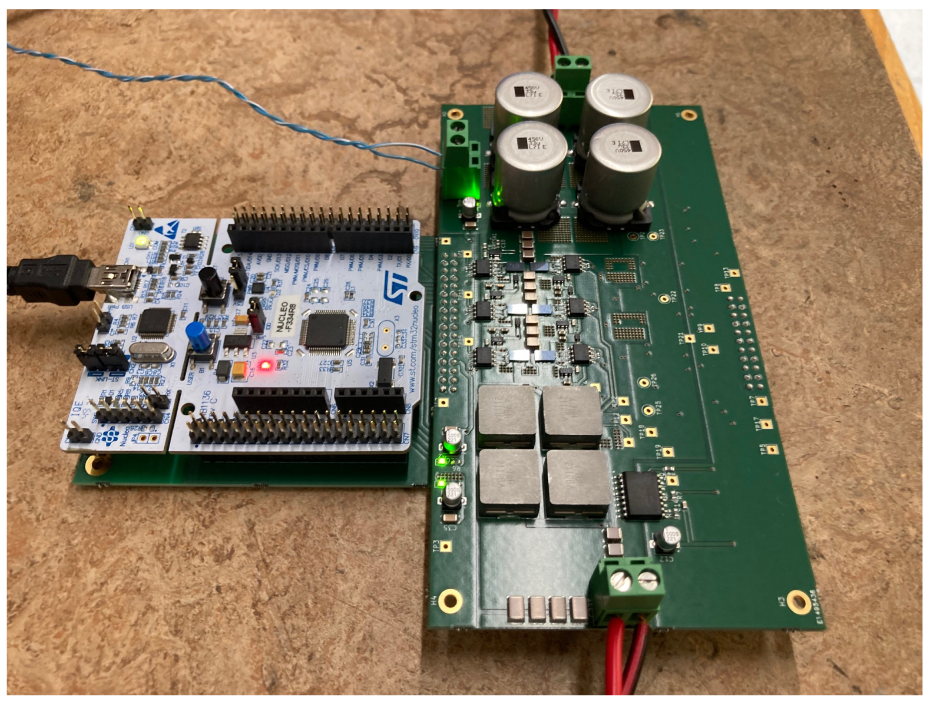
In order to verify this finding, the circuit of Figure 1 is simulated in the Matlab-Simulink© v. 23.2 environment, using the PLECS© v. 4.8.3 toolbox and considering, wherever applicable, the circuit parameters reported in Table 1.
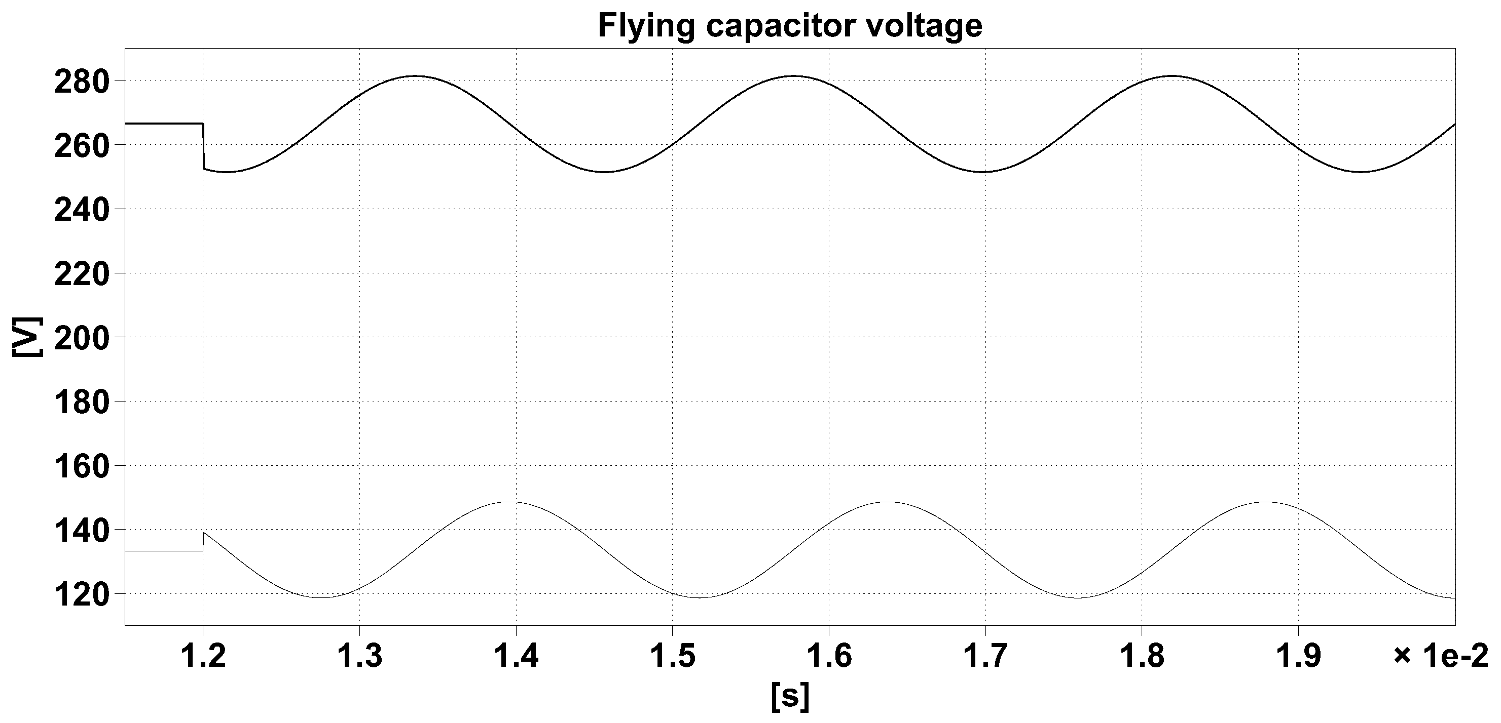
The simulation results are shown in Figure 4, considering D = 0.25 and perturbation values of + 3.5 % on v C 1 and 3.5 % on v C 2 , applied at t = 12 m s , when the circuit is operating in the steady state. For better readability, the switching ripple is removed from the traces using a moving average filter.
If we use (23) to calculate the frequency of the oscillation when D = 0.25 as in Figure 4, we find 420 Hz , a value that is very close to the one resulting from the simulation plot of Figure 4, that is 418 Hz . It is also interesting to notice how the oscillating voltage waveforms correspond to sine and cosine terms as implied by the presence of purely imaginary, complex conjugate eigenvalues. Finally, it is important to point out that the average modeling approach is well posed and reliable, as the oscillation period of the dynamic phenomena under investigation is much longer than the averaging period. Now, we need to verify if the same conclusions can be drawn for region R 2 and R 3 .  

2.5.2. Analysis of the Circuit in Region R 2 and R 3

The procedure to derive the dynamic model of the flying capacitor cells in region R 2 and R 3 is basically the same as that followed for R 1 . The only difference is that now we need to use matrices C C 2 T and C C 3 T , respectively, to identify the integration intervals and the polarity of the capacitor insertions. The system of differential Equation (22) turns out to be identical to the previous one, except for the eigenvalue expression, which, for region R 2 is found to be
λ 2 = f 2 ( D ) T s w 2 L C f , with f 2 ( D ) = 1 3 + 2 D 2 D 2 ,
while for region R 3 it is equal to
λ 3 = f 3 ( D ) T s w 2 L C f , with f 3 ( D ) = 1 D 2 ,
again under the simplifying assumption of having identical flying capacitors values. It is interesting to observe that the three f r ( D ) functions, with  r [ 1 , 2 , 3 ] , once composed in the interval D [ 0 , 1 ] , correspond to a function that is not only continuous but continuously differentiable as well.
In conclusion, the system exhibits essentially the same dynamic behavior of region R 1 in R 2 and R 3 as well, only with different resonance frequencies. 
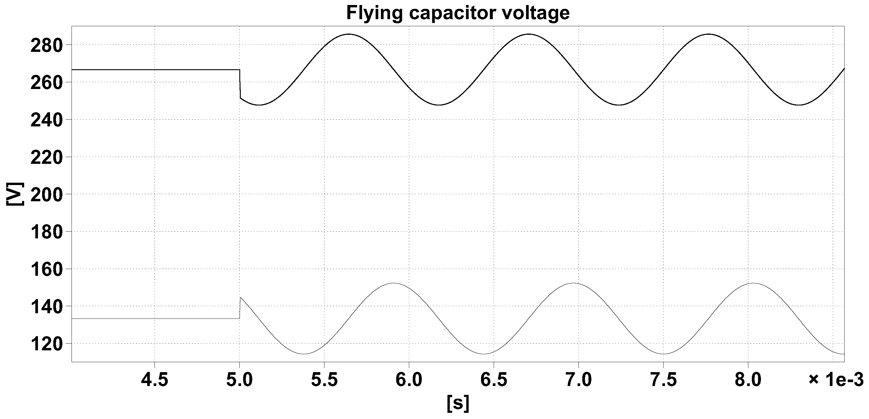
Figure 5 displays the results of test simulations with D = 0.61 and perturbation values of + 5 % on v C 1 and 5 % on v C 2 , applied at t = 5 m s . The oscillation frequency predicted as λ 2 / 2 π is equal to 957 Hz , while the one found simulating the circuit is 951 Hz . Finally, 
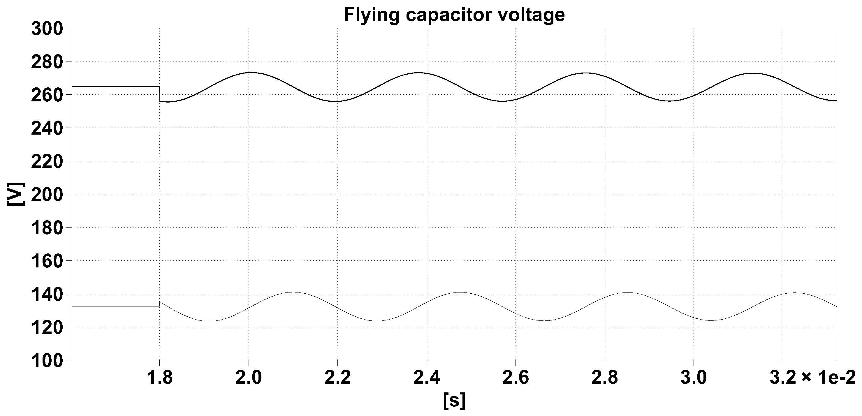
Figure 6 displays the results of the test simulations with D = 0.8 and perturbation values of 2.5 % on v C 1 and + 2.5 % on v C 2 , applied at t = 18 m s . The oscillation frequency predicted as λ 3 / 2 π is equal to 269 Hz , while the one found simulating the circuit is 267 Hz . The oscillation frequencies observed in the simulation only depend on the parameters appearing in (23)–(25); they are practically invariant for a different input voltage, average inductor current or perturbation sign, and amplitude.

2.6. Generalization of the Flying Capacitor Cell Dynamic Model

The above modeling approach can be likewise applied to higher-order converters. The main limitation is that the required pencil and paper calculations become more and more involved; in order to prevent errors, a Matlab© script is implemented to automate the derivation of the system state matrix A r in all converter operating regions and, in principle, for any value of N. The key step is the automatic construction of the inductor current integrals in each sub-interval. Indeed, as can be seen in (18) and (20), the average flying capacitor current is obtained exactly by summing the inductor current integrals over each sub-interval, which, assuming the current to be piecewise linear, correspond to a trapezoidal integration process. The integration routine can therefore be built from (9) as a sequence of repeated summations followed by multiplication between the resulting integration matrix and the time weighted capacitor connection matrix (9). The adopted algorithm is reported in Appendix A for better clarity. It is tested on values of N ranging from 4 to 9, yielding consistent results.
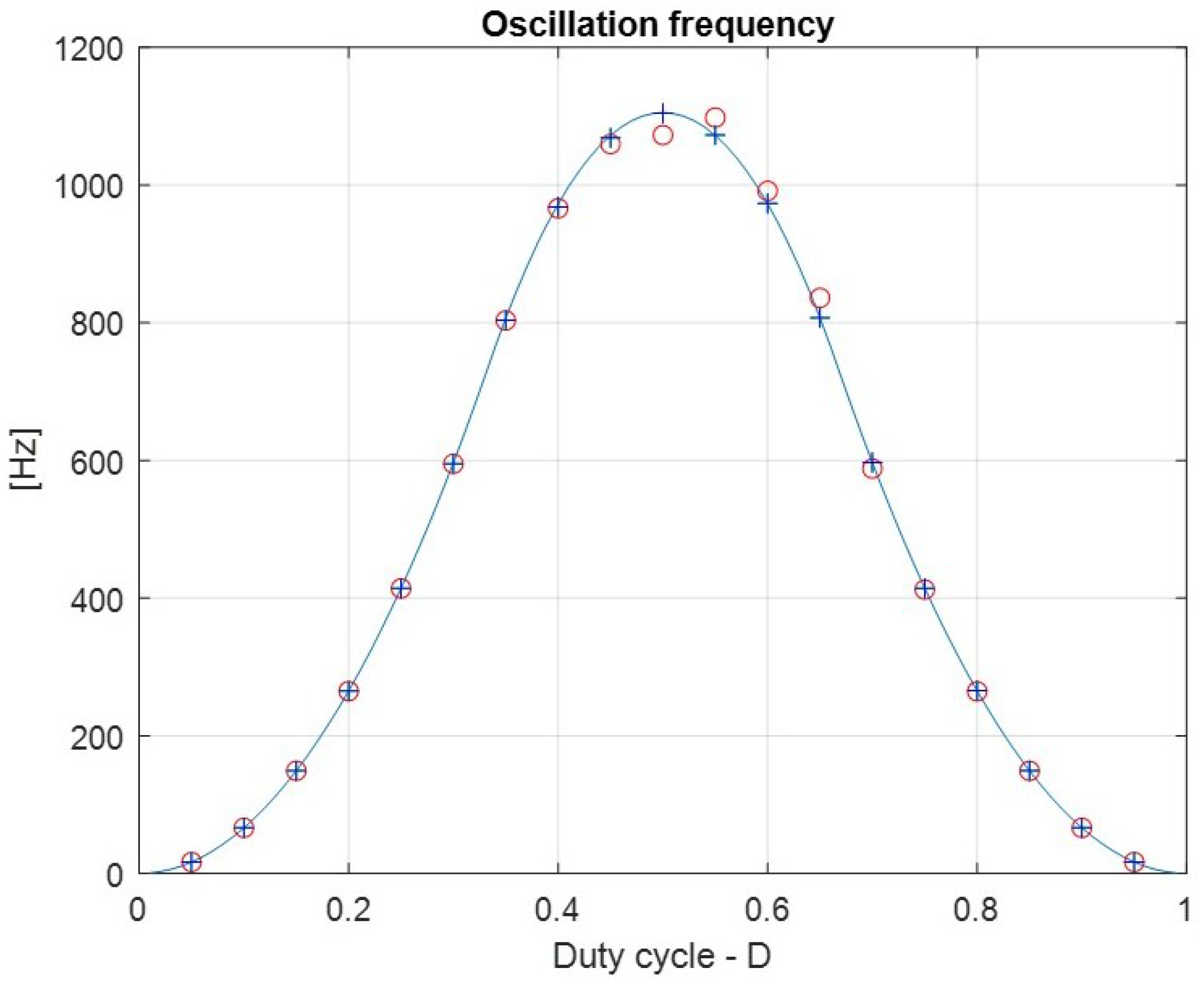
Thanks to this procedure, it is then possible to derive the expressions of the system eigenvalues in each operating region and to calculate, among other things, the magnitude plot shown in Figure 7 also for higher values of N. The figure is obtained comparing the analytically calculated eigenvalue magnitude with the oscillation frequency automatically extracted from simulation plots like those in Figure 4, Figure 5 and Figure 6. This step is facilitated by the insertion of losses in the circuit, especially at duty cycles around 0.5, where strong beating occurs, complicating the automatic extraction of the oscillation frequency.
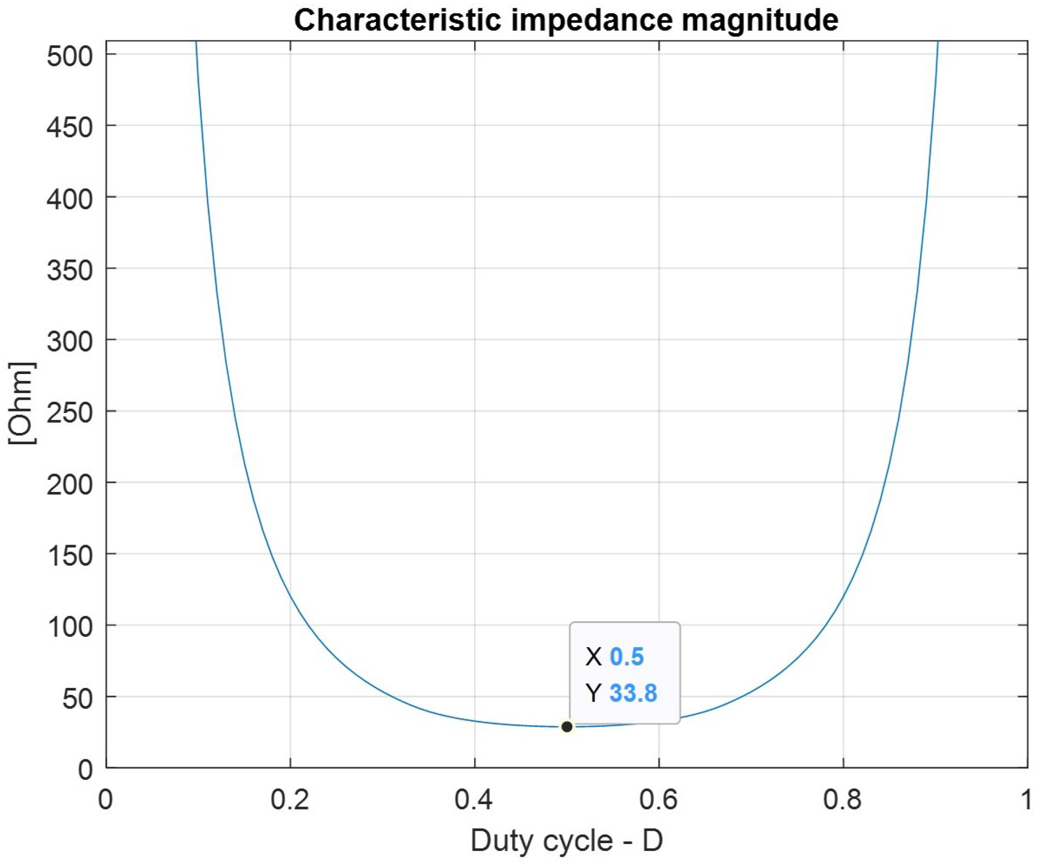
From the automated modeling, it is also possible to determine the magnitude of the characteristic impedance associated with the resonant poles in the circuit. This can be directly extrapolated from (23)–(25), and it is found to be given by
| Z c h r r | = 2 L f s w f r ( D ) ,
where f r ( D ) with r [ 1 , 2 , 3 ] is the specific dependency from the duty cycle D of expressions (23)–(25). The plot of | Z c h r | over the whole duty-cycle range is shown in Figure 8.
As can be seen, a minimum value of about 34 Ω is found for D = 0.5 . The plot confirms the observed tendency of the circuit to oscillate more widely and with longer transients when the duty cycle is around 0.5 . It also allows to estimate the value of a possible damping resistor.
Considering the values of (26), we see that placing in parallel to each flying capacitor an AC coupled damping resistor of about 100 Ω should be sufficient to visibly shorten the transient duration over the entire operating range. Given the observed typical amplitude of the oscillations, a small amount of additional losses is going to be generated, estimated at around 1 W per cell (only during transients, of course).

3. Experimental Validation

The dynamic model illustrated in Section 2, differently from prior art, predicts the existence of natural oscillation modes resulting from the interaction between the inductor and the flying capacitor cells in any FCML boost converter. These modes have been characterized analytically and at the simulation level, but the experimental validation of the analysis is now due. A prototype of the circuit in Figure 1 is therefore set up and can be seen in Figure 9. The main circuit parameters are listed in Table 1. The switching cells use 200 V , 48 A rated EPC 2034C GaN devices. Overall, the cells occupy a 50 m m × 28 m m area. The power circuit is coupled to a digital control board that uses the STM32F334R8 microcontroller for modulation and higher-level control functions.

3.1. Flying Capacitor Voltage Sensing

A distinctive feature of the developed hardware is the presence of flying capacitor voltage sensors. Different from what can be read in many papers, sensing the flying capacitor voltages can have minimal impact on the circuit power density and reliability. The proposed solution is shown in Figure 10. As can be seen, the circuit uses a simple pnp-BJT to derive a power ground referred signal that is then amplified and transferred to the signal ground referred domain by a standard isolation amplifier. Because the bias current of the transistor can be set very low (e.g., 0.1 m A ) adjusting resistors R B 1 i and R B 2 i on each cell, the power dissipation of the sensor is well below 0.1 W , which can be deemed negligible in many applications. Furthermore, adjusting the values of the collector resistors R C i on each cell, it is possible to scale the measured voltage so that, when the flying capacitors are balanced, the voltage at the input of the ADC is practically the same for every cell, which makes the subsequent processing easier. The impact of the isolation amplifier on the circuit power consumption is estimated by supplying the primary and secondary sides from external power supplies and measuring the current. Overall, less than 1 W is needed, which also includes the sensing of the other circuit state variables, i.e., the inductor current and the output voltage. Again, unless the circuit is designed for low-power applications, this negligibly impacts the circuit power consumption.

3.2. Flying Capacitor Voltage Damping

Thanks to the availability of a sensor, it is possible to measure the flying capacitor voltages without any risk during circuit operation. This allows us to experimentally validate the results presented in Figure 7. In order to do so, we simply apply relatively small duty-cycle steps during the converter open-loop operation, which stimulates the resonance and allows to record the transient with a digital oscilloscope.
It is worth noting that the power circuit includes passive R-C snubbers, placed in parallel to each flying capacitor, and aimed at dampening the above-mentioned oscillations. The snubbers are designed based on the above circuit analysis; as can be seen in Figure 11, their effectiveness is good, as the oscillations are indeed decaying very rapidly (practically extinguishing themselves in about three cycles, even around D = 0.5 , which represents the worst case). Because this solution is inexpensive and has limited impact on the converter footprint, it represents a simple way to contain the resonance phenomenon, although with a negative impact on the efficiency.
In order to quantify this, the circuit efficiency is measured and found to be practically flat around 98 % throughout the load range as shown in Figure 12, indicating that the circuit is not excessively lossy, even if snubbers and sensors are used. Indeed, thermal analysis shows the losses to be mostly concentrated on the switches, while snubbers maintain a relatively low temperature. On the other hand, the damping action makes the circuit much safer to operate, as it prevents significant deviations of the flying capacitor voltages with respect to their expected values, especially in the case of input voltage variations. This helps to limit the switches’ voltage stress, which could potentially lead to circuit failure.
As a downside, the presence of damping makes measuring the natural oscillation frequency of the resonant circuit more complicated. A first-order estimation is, anyway, still possible, as the circuit Q factor can be approximately found from the amplitude speed of decay. In our case, some post-processing of the acquired data yields a Q factor between 2 and 3, determining an underestimation of the resonant pole frequency in the order of 8–10% with respect to the first oscillation period. Applying this correction to the gathered experimental plots, the resonance frequencies at different operating points are found. They are also plotted in Figure 11, where the experimentally determined resonant mode map (represented as green boxes, to account for measurement uncertainties) is compared to the analytical one.
The oscillation tests are performed at different operating points, including different input voltages. As expected from the analytical study, the average voltage level is irrelevant in defining the oscillation frequencies, which are practically the same for a given duty cycle, regardless of the specific input voltage level or the load condition (the load condition has a strong impact on the damping of the inductor resonance with the output capacitor but not on the oscillation frequency of the flying capacitors.). As can be seen, the measurements made at relatively low input voltages confirm the trend and, considering the uncertainty of the experimental procedure, also show a reasonable quantitative match with the analytical results.

3.3. Active Damping of the Flying Capacitor Cells

The hardware organization of the prototype is such that it becomes possible to implement the active damping of the flying capacitor dynamics, complementing the passive one and, possibly, further improving the circuit dynamic performance. In addition, the adoption of combined active and passive damping can also allow to relax the R-C snubber design, with a positive impact on efficiency.
Figure 13 shows a possible active damping controller organization, which is particularly simple and, as such, computationally light. As proposed in [12], this compensation can be thought of as a parallel regulation loop that complements the modulator and, if properly designed, can be transparent to any other control loop. For this to happen, some decoupling is needed between the damping loop and, mostly, the current control loop. In practice, we expect that a reasonable spectral decoupling can be achieved by making the current loop significantly faster than the damping loop.
As can be deduced from the discussion in Section 2.1, the average voltage over the flying capacitor C i can be adjusted by introducing some difference in the conduction times of the two adjacent switches S i b and S ( i + 1 ) b . Therefore, the controller organization is such that, when the flying capacitor voltages are balanced, the correction is zero and each cell operates with the same duty cycle. Instead, when some unbalance or oscillation is detected, the controller makes the cell duty cycles slightly different, as needed to reduce the error. In principle, different regulator structures can be considered, the simplest being the purely proportional one, which is certainly effective also against the static unbalance.
Another solution is to implement a derivative action (actually, in the practical implementation, a digital low pass filter is also used so as to suppress the derivative action above 1/10 of the converter modulation frequency), which turns out to be particularly effective in dampening the oscillations. An intuitive explanation is that such a regulator tends to change the average flying capacitor voltage (correcting the duty cycle) in a way that is proportional to the current through it, an action that tends to emulate a virtual series resistor.
Controller calibration requires a trial-and-error procedure, as both the resonance frequency and the characteristic impedance of the resonant circuit vary significantly with the duty cycle, calling for a trade-off solution. This controller is therefore easier to apply if the operating point of the converter, namely, its input and output voltages, is not changing too much. Instead, for a successful application in cases where the converter’s operating point is significantly changing over time, the on-line adaptation of the derivative gain can be considered, which can be simply implemented by means of a look-up table, possibly using the converter duty cycle as the entry. A couple of examples of the achievable performance are shown in Figure 14 and Figure 15.
As can be seen, the derivative control action is indeed able to suppress the oscillations induced by the duty-cycle step. In agreement with the above discussion, the discrete-time derivative gain coefficient is designed so that, considering all the scaling factors of the experimental set-up and a sampling frequency equal to f s w , it corresponds to a virtual series resistance around 100 Ω in the nominal operating conditions ( V I = 200 V , V O = 400 V ) as per
k d j = C f ( 1 D ) R d m p f s w V C j , j [ 1 , 2 ] ,
where R d m p represents the above-specified virtual damping resistor and V C 1 , 2 are the steady-state values of the flying capacitor voltages when the converter operates at duty cycle D.
The natural decoupling of the active damping action, as expected, is not always satisfactory: small oscillations of the output current become visible in Figure 14b and Figure 15b when the function is activated. This downside could be minimized by closing a current control loop, which is not considered in this paper, for the reasons explained above. Despite that, the combination of active and passive damping seems to be quite effective in mitigating the flying capacitor oscillatory response.

4. Conclusions

This paper discusses the flying capacitor dynamic behavior in boost type FCML DC-DC converters. The main contributions made are the following:
  • A newly conceived dynamic model that is capable of predicting the interaction between the input inductor and the flying capacitors, allowing to determine the natural oscillation frequencies of the flying capacitor cell subsystem;
  • A passive damping solution that strongly improves the flying capacitor dynamics with minimal impact on the circuit power consumption;
  • A simple sensing technique for flying capacitor voltages that allows to implement, if needed, active damping control strategies, unbalance detection, and/or converter protection mechanisms;
  • An example of derivative-type active compensation that effectively suppresses the flying capacitor oscillations.
The dynamic model is validated both at the simulation level and experimentally. The active and passive damping strategies are also experimentally validated and proved effective in mitigating the oscillatory response of the circuit.

Author Contributions

Conceptualization, S.B. and L.R.; methodology, S.B. and L.R.; software, S.B.; validation, S.B.; formal analysis, S.B.; investigation, S.B.; data curation, S.B.; writing—original draft preparation, S.B.; writing—review and editing, S.B. All authors have read and agreed to the published version of the manuscript.

Funding

This research received no external funding.

Data Availability Statement

The raw data supporting the conclusions of this article come from a proprietary converter prototype. Requests to access the datasets should be directed to the authors, but are subject to restrictions as those data are part of an ongoing study.

Conflicts of Interest

The authors declare no conflicts of interest.

Appendix A

The switching matrices for a four-level FCML boost converter under PSPWM are the following:
S 1 = 1 0 0 0 0 0 0 0 1 0 0 0 0 0 0 0 1 0 , S 2 = 1 1 1 0 0 0 0 0 1 1 1 0 1 0 0 0 1 1 , S 3 = 1 1 1 1 1 0 1 0 1 1 1 1 1 1 1 0 1 1 .
The capacitor connection matrices are
C C 1 = 1 0 1 0 0 0 0 0 1 0 1 0 1 1 1 1 0 1 , C C 2 = 1 1 0 1 1 0 1 0 1 1 0 1 0 1 1 1 0 0 , C C 3 = 0 1 0 0 0 1 0 1 0 1 0 0 0 0 0 1 0 0 .

Appendix Automated Model Set-Up Procedure

The automatic computation of the system state matrices can be obtained by calculating the trapezoidal integration matrices from the connection matrices C C i using the following script:
for i=1:size(CC1,1)
 for j=size(CC1,2):-1:1
  TINT1(i,j) = CC1T(i,j);
  % TINT is the trapezoidal integration matrix
  for k = j-1:-1:1
   TINT1(i,j) = TINT1(i,j) + 2*CC1T(i,k);
  end
end
end
which refers to region R 1 . After that, the state matrix A 1 can be automatically determined as per
% calculation of matrix A_1 
A1 = zeros(N-2);
for i=1:(N-2)+1
for j=1:(N-2)+1
  for k=1:(2*N-2)
   A1(i,j) = A1(i,j) - CC1T(i,k)*TINT1(j,k);
  end
end
end
A1v = ON*A1;
In the above script, the dimension scaling matrix O N is given by
O N = diag T s w 2 L C i , i [ 1 , N 2 ] .
that is a ( N 2 ) × ( N 2 ) purely diagonal matrix with the indicated elements. Completely similar scripts determine the state matrix A in regions 2 and 3.
The typical choice C i = C f i yields a complex conjugate, purely imaginary eigenvalues of multiplicity equal to ( N 2 ) / 2 when N 2 is even, or else, when N 2 is odd, the same plus a single null eigenvalue. As an example, for N = 5 , the O N matrix is
O N = T s w 2 L C 1 0 0 0 T s w 2 L C 2 0 0 0 T s w 2 L C 3
while, after running the above scripts, the flying capacitor cell eigenvalues in region R r are λ r 1 = 0 , λ r 2 , 3 = ± i · f r ( D ) T s w 2 L C f , with
f r ( D ) = ( 2 ) D 2 r = 1 ( 2 ) D 2 D + 1 / 8 r = 2 ( 2 ) D 2 D + 1 / 8 r = 3 ( 2 ) 1 D 2 r = 4 .
corresponding to an oscillation frequency plot very similar in shape to the one shown in Figure 7.

References

  1. Lei, Y.; Barth, C.; Qin, S.; Liu, W.C.; Moon, I.; Stillwell, A.; Chou, D.; Foulkes, T.; Ye, Z.; Liao, Z.; et al. A 2-kW Single-Phase Seven-Level Flying Capacitor Multilevel Inverter with an Active Energy Buffer. IEEE Trans. Power Electron. 2017, 32, 8570–8581. [Google Scholar] [CrossRef]
  2. Liao, Z.; Lei, Y.; Pilawa-Podgurski, R.C.N. Analysis and Design of a High Power Density Flying-Capacitor Multilevel Boost Converter for High Step-Up Conversion. IEEE Trans. Power Electron. 2019, 34, 4087–4099. [Google Scholar] [CrossRef]
  3. Huang, Q.; Ma, Q.; Liu, P.; Huang, A.Q.; de Rooij, M.A. 99% Efficient 2.5-kW Four-Level Flying Capacitor Multilevel GaN Totem-Pole PFC. IEEE J. Emerg. Sel. Top. Power Electron. 2021, 9, 5795–5806. [Google Scholar] [CrossRef]
  4. Wilkinson, R.H.; Meynard, T.A.; du Toit Mouton, H. Natural Balance of Multicell Converters: The Two-Cell Case. IEEE Trans. Power Electron. 2006, 21, 1649–1657. [Google Scholar] [CrossRef]
  5. Qin, S.; Lei, Y.; Ye, Z.; Chou, D.; Pilawa-Podgurski, R.C.N. A High-Power-Density Power Factor Correction Front End Based on Seven-Level Flying Capacitor Multilevel Converter. IEEE J. Emerg. Sel. Top. Power Electron. 2019, 7, 1883–1898. [Google Scholar] [CrossRef]
  6. Thielemans, S.; Ruderman, A.; Reznikov, B.; Melkebeek, J. Improved Natural Balancing with Modified Phase-Shifted PWM for Single-Leg Five-Level Flying-Capacitor Converters. IEEE Trans. Power Electron. 2012, 27, 1658–1667. [Google Scholar] [CrossRef]
  7. Stillwell, A.; Candan, E.; Pilawa-Podgurski, R.C.N. Active Voltage Balancing in Flying Capacitor Multi-Level Converters with Valley Current Detection and Constant Effective Duty Cycle Control. IEEE Trans. Power Electron. 2019, 34, 11429–11441. [Google Scholar] [CrossRef]
  8. Ye, Z.; Lei, Y.; Liao, Z.; Pilawa-Podgurski, R.C.N. Investigation of Capacitor Voltage Balancing in Practical Implementations of Flying Capacitor Multilevel Converters. IEEE Trans. Power Electron. 2022, 37, 2921–2935. [Google Scholar] [CrossRef]
  9. McGrath, B.P.; Holmes, D.G. Analytical Modelling of Voltage Balance Dynamics for a Flying Capacitor Multilevel Converter. IEEE Trans. Power Electron. 2008, 23, 543–550. [Google Scholar] [CrossRef]
  10. Xu, Y.; Wang, J.; Xiong, K.; Yin, G. A Novel 5-Level Flying Capacitor Bridgeless PFC Converter Based on Cost-Effective Low-Voltage eGaN FETs. Chin. J. Electr. Eng. 2020, 6, 56–64. [Google Scholar] [CrossRef]
  11. Petric, I.Z.; Iyer, R.K.; Brooks, N.C.; Pilawa-Podgurski, R.C.N. A Real-Time Estimator for Capacitor Voltages in the Flying Capacitor Multilevel Converter. In Proceedings of the 2022 IEEE 23rd Workshop on Control and Modeling for Power Electronics (COMPEL), Tel Aviv, Israel, 20–23 June 2022; pp. 1–8. [Google Scholar] [CrossRef]
  12. Iyer, R.K.; Petric, I.Z.; Bayliss, R.S.; Brooks, N.C.; Pilawa-Podgurski, R.C.N. A High-Bandwidth Parallel Active Balancing Controller for Current-Controlled Flying Capacitor Multilevel Converters. In Proceedings of the 2023 IEEE Applied Power Electronics Conference and Exposition (APEC), Orlando, FL, USA, 19–23 March 2023; pp. 775–781. [Google Scholar] [CrossRef]
  13. Farivar, G.; Ghias, A.M.Y.M.; Hredzak, B.; Pou, J.; Agelidis, V.G. Capacitor Voltages Measurement and Balancing in Flying Capacitor Multilevel Converters Utilizing a Single Voltage Sensor. IEEE Trans. Power Electron. 2017, 32, 8115–8123. [Google Scholar] [CrossRef]
  14. Wu, J.; Lu, Y. Decoupling and Optimal Control of Multilevel Buck DC-DC Converters with Inverse System Theory. IEEE Trans. Ind. Electron. 2020, 67, 7861–7870. [Google Scholar] [CrossRef]
  15. Lin, B.R.; Huang, C.H. Implementation of a Three-Phase Capacitor-Clamped Active Power Filter Under Unbalanced Condition. IEEE Trans. Ind. Electron. 2006, 53, 1621–1630. [Google Scholar] [CrossRef]
  16. Liu, X.; Mok, P.K.T.; Jiang, J.; Ki, W.H. Analysis and Design Considerations of Integrated 3-Level Buck Converters. IEEE Trans. Circuits Syst. I Regul. Pap. 2016, 63, 671–682. [Google Scholar] [CrossRef]
  17. Yousefzadeh, V.; Alarcon, E.; Maksimovic, D. Three-level buck converter for envelope tracking applications. IEEE Trans. Power Electron. 2006, 21, 549–552. [Google Scholar] [CrossRef]
  18. Abdelhamid, E.; Bonanno, G.; Corradini, L.; Mattavelli, P.; Agostinelli, M. Stability Properties of the 3-Level Flying Capacitor Buck Converter Under Peak or Valley Current Programmed Control. IEEE Trans. Power Electron. 2019, 34, 8031–8044. [Google Scholar] [CrossRef]
  19. Brooks, N.C.; Iyer, R.K.; Bayliss, R.S.; Pilawa-Podgurski, R.C.N. Fundamental State-Space Modeling Methodology for the Flying Capacitor Multilevel Converter. In Proceedings of the 2022 IEEE 23rd Workshop on Control and Modeling for Power Electronics (COMPEL), Tel Aviv, Israel, 20–23 June 2022; pp. 1–7. [Google Scholar] [CrossRef]
  20. Xia, Z.; Datta, K.; Stauth, J.T. State-Space Modeling and Control of Flying-Capacitor Multilevel DC–DC Converters. IEEE Trans. Power Electron. 2023, 38, 12288–12303. [Google Scholar] [CrossRef]
Figure 1. Schematic representation of a four-level, flying capacitor boost DC-DC converter.
Electronics 13 04883 g001
Figure 2. Modulation patterns for N = 4 (left); inductor and flying capacitor currents (right). For Region R 1 , the switching state matrix (5) is also indicated in blue (top left). Please note that the inductor current waveform is exactly the same any time the duty cycle considered for each region is set at the same distance from the boundaries.
Electronics 13 04883 g002
Figure 3. Effect of flying capacitor unbalanced voltages for N = 4 and in region R 1 . Encircled numbers indicate the sub-intervals of the considered modulation period.
Electronics 13 04883 g003
Figure 4. Effects of flying capacitor voltage perturbation in Region R 1 with D = 0.25 . The flying capacitor average voltages oscillate at 418 Hz around their nominal values V C 1 = 133 V , V C 2 = 267 V .
Electronics 13 04883 g004
Figure 5. Effects of flying capacitor voltage perturbation in Region R 2 with D = 0.61 . The flying capacitor average voltages oscillate at 951 Hz around their nominal values.
Electronics 13 04883 g005
Figure 6. Effects of flying capacitor voltage perturbation in Region R 3 with D = 0.8 . The flying capacitor average voltages oscillate at 267 Hz around their nominal values.
Electronics 13 04883 g006
Figure 7. Plot of the oscillation frequency as a function of the converter duty cycle D. The solid line represents (23)–(25). Circles indicate time domain simulation results with no losses, and crosses indicate the same results in a lossy circuit.
Electronics 13 04883 g007
Figure 8. Magnitude of the resonant poles characteristic impedance for N = 4 . The minimum is found at D = 0.5 and is equal to 33.8 Ω .
Electronics 13 04883 g008
Figure 9. Microcontroller and power converter board assembly.
Electronics 13 04883 g009
Figure 10. Schematic of the i-th flying capacitor voltage transducer. A BJT (pnp type) and an isolation amplifier are used to scale down and transfer the flying capacitor voltages from the power domain to the signal domain.
Electronics 13 04883 g010
Figure 11. Experimentally measured oscillation modes, compared to the theoretically determined ones. On the right, two examples of time domain flying capacitor waveforms. The red trace corresponds to the voltage across flying capacitor C 1 . The scale factor is 60 V / V 6 V / d i v . The green trace is the load current ( 100 m V / A 1 A / d i v ) .
Electronics 13 04883 g011
Figure 12. Measured circuit efficiency at nominal input and output voltage as a function of the applied load.
Electronics 13 04883 g012
Figure 13. Block diagram of the active damping control function. Regulators can be identical for the two loops; only the gain is individually adjusted.
Electronics 13 04883 g013
Figure 14. Experimentally measured oscillations before (a) and after (b) the application of the active damping algorithm. The red trace corresponds to the voltage across flying capacitor C 2 . The scale factor is 120 V / V 24 V / d i v . The green trace is the load current ( 100 m V / A 1 A / d i v ) .
Electronics 13 04883 g014
Figure 15. Experimentally measured oscillations before (a) and after (b) the application of the active damping algorithm. The red trace corresponds to the voltage across flying capacitor C 2 . The scale factor is 120 V / V 24 V / d i v . The green trace is the load current ( 100 m V / A 1 A / d i v ) .
Electronics 13 04883 g015
Table 1. FCML converter circuit parameters.
Nominal output voltage400 V
Nominal output power1 kW
Nominal input voltage200 V
Number of levels4
Switching frequency150 kHz
Input inductor18.8 μH
Flying capacitors4.2 μF
Snubber capacitors10 μF
Snubber resistors100 Ω
Disclaimer/Publisher’s Note: The statements, opinions and data contained in all publications are solely those of the individual author(s) and contributor(s) and not of MDPI and/or the editor(s). MDPI and/or the editor(s) disclaim responsibility for any injury to people or property resulting from any ideas, methods, instructions or products referred to in the content.

