Article

TCAD Simulation of an E-Mode Heterojunction Bipolar p-FET with Imax > 240 mA/mm

1
School of Information Science and Technology, Nantong University, Nantong 226019, China
2
Jiangsu Key Laboratory of Semiconductor Device & IC Design, Package and Test, School of Microelectronics and Integrated Circuits, Nantong University, Nantong 226019, China
3
School of Electronic Science and Engineering, Nanjing University, Nanjing 210093, China
*
Authors to whom correspondence should be addressed.
Electronics 2024, 13(23), 4752; https://doi.org/10.3390/electronics13234752
Submission received: 29 October 2024 / Revised: 27 November 2024 / Accepted: 29 November 2024 / Published: 1 December 2024

Abstract

:
This work demonstrates an enhancement mode heterojunction bipolar p-FET (HEB-PFET) structure with a AlGaN/GaN heterojunction bipolar transistor (HBT) integrated on the drain side. Such device design notably contributes to the ultra-high output current density, which is conventionally limited by the low hole mobility and concentration in the p-FETs. The HEB-PFET exhibits an output current density of 241 mA/mm, which is 134 times larger compared to the conventional p-FET (C-PFET) and 2.4 times of the homojunction bipolar p-FET (HOB-PFET). This can be attributed to a better current gain of HBT than homojunction bipolar transistor (BJT). An optimized HEB-PFET of 6 nm p-GaN layer beneath the gate is proposed, where ION/IOFF is >1011, and Vth is −0.44 V. Additionally, thermal stabilities are studied with temperature changes from 300 K to 425 K. Moreover, a semi-empirical compact model is presented to visually explain the working principle of the HEB-PFET.
Keywords:
p-FET; GaN; HBT; TCAD

1. Introduction

Gallium nitride (GaN), as an emerging wide bandgap semiconductor material, is regarded as a key material to promote the development of the next generation of high-efficiency and high-frequency electronic devices because of its outstanding electron mobility and high breakdown electric field strength [1]. With the maturity of GaN n-channel high-electron mobility transistor (HEMT) technology, considerable performance improvements have been brought to the fields of power electronics, radio frequency applications, and high-speed digital circuits. GaN-based complementary metal oxide semiconductor (CMOS) technology combines the wide-band gap characteristics of GaN with the low static power consumption advantages of CMOS, showing significant potential in promoting the development of integrated circuits (ICs). The GaN-based power and associated peripheral devices in use today are solely reliant on n-channel, meaning that integrated logic circuits cannot leverage the most power-saving complementary logic solutions that are prevalent in Si logic ICs [2]. Therefore, the fabrication of E-mode GaN p-channel field-effect-transistors (p-FETs) has become crucial to fully exploit the performance of GaN CMOS technology, which not only improves circuit switching speed and reduces static power consumption [2,3,4] but also simplifies circuit design for safer and more reliable operation.
However, the severe mismatch in current density driving capability between p-FETs and n-HEMTs is the primary obstacle to achieving high-performance GaN-based CMOS logic circuits. The average hole mobility of GaN p-FETs at room temperature is about 16 cm2/V·s [5,6], which is much smaller than the electron mobility (>1000 cm2/V·s) due to the large hole effective mass. Additionally, p-GaN layer is often achieved by doping magnesium (Mg), where Mg has an activation rate of only 2–3% at room temperature [7], making it challenging to realize the high concentration of holes. Thus, it is a knotty task to obtain GaN based p-FETs with high output drain current density (ID). To address these issues, some researchers have confirmed that optimization of heterojunctions can effectively improve the output characteristics of GaN p-channel devices, including (1) AlN/GaN [8,9] (2) InGaN/GaN [5,10] (3) GaN/AlInGaN [11,12]. However, the problem is that they cannot be integrated with the mainstream commercial n-HEMTs. Therefore, from the perspective of GaN ICs integration, the GaN/AlGaN heterojunction structure is preferred for the design of GaN p-FETs. Considering the safety and circuit design simplification, enhancement mode p-FETs are preferred. Several studies have been reported to achieve enhancement device, in which devices with recessed gate are widely used [13,14]. The recessed gate is formed by etching the p-type layer beneath the gate to deplete the 2DHG channel under the gate, ensuring that the device is depleted at the off-state. Other methods to achieve enhancement mode include oxygen (hydrogen) plasma treatment [15], n-GaN [16] or n-AlGaN gate cap [17], and hybrid barrier layer [5].
GaN/AlGaN heterojunction-based P-FETs are more attractive because this structure can monolithically integrate with the predominant commercial p-GaN gate-enhanced GaN HEMTs. However, the output current density is around 20 mA/mm in the enhancement devices, which is too small to integrate with GaN based HEMTs [7,13,14,17,18,19]. In order to improve the performance of enhancement mode GaN/AlGaN p-FET, Yang et al. [18] reported enhancement-mode p-channel heterojunction field–effect transistors without gate recess on a standard p-GaN/AlGaN/GaN high electron mobility transistor platform, obtaining a drain current density of 0.2 mA/mm and a threshold voltage of −0.6 V. And Raj et al. [19] proposed GaN/AlGaN superlattice-based normally-off hole channel FinFET devices, characterized by a current density of 13 mA/mm and a threshold voltage of −0.2 V. More recently, Tang et al. [20] have introduced an innovative approach to increase the output current density by adding a NPN bipolar stack of n-/p-/n-GaN on the drain side of the p-FET and enhanced the conduction capability by converting electrons into the main carriers, and obtaining a threshold voltage of −2 V through the recessed gate, with an output current density of 120 mA/mm. In this work, a GaN-based p-FET is proposed on the conventional p-GaN HEMT platform, and a GaN/AlGaN heterojunction is used to form two-dimensional hole gas (2DHG). Additionally, a heterojunction bipolar structure is proposed on the drain side of the device. The electric characteristics of the proposed HEB-PFET have been studied and compared with HOB-PFET and C-PFET. The simulation results show that the HEB-PFET exhibits the largest output drain current density, this can be ascribed to a larger current density gain of HBT. Both devices show a good gate control ability, where the leakage current density is less than 10−8 mA/mm and the ION/IOFF ratio reaches 1011. In addition, the p-GaN layer beneath the gate is recessed to obtain enhancement mode, and the thermal stability of the proposed device is also studied. Moreover, to improve understanding and predictability of the proposed HEB-PFET, a semi-empirical compact model of the output current density ID of the device is given.

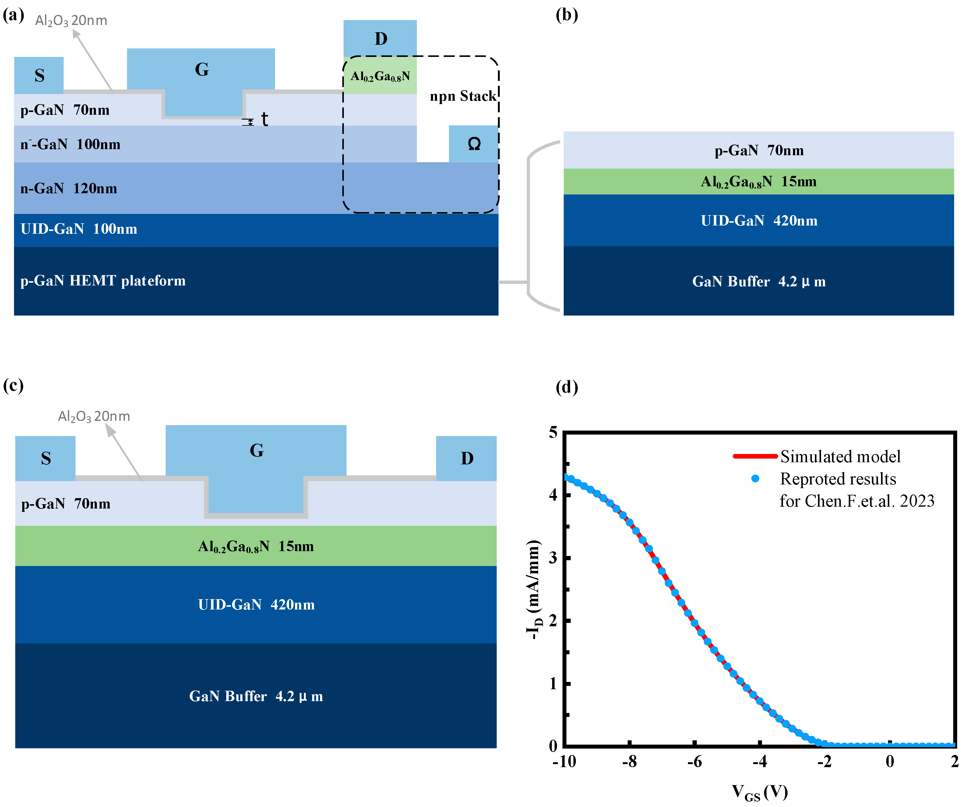
2. Device Structure and Simulation Models

Figure 1a,b exhibit a schematic of the proposed HEB-PFET and a commercial p-GaN HEMT platform, respectively. The commercial p-GaN HEMT platform consists from top to bottom of a 70 nm p-GaN layer doped with a Mg concentration of 2 × 1019 cm−3, a 6 nm p-GaN layer underneath the gate (t), a 15 nm Al0.2Ga0.8N barrier layer doped with Si concentration of 5 × 1016 cm−3, a 420 nm unintentionally doped GaN (UID-GaN) layer, and 4.2 μm GaN buffer layer on a substrate. A recessed gate is introduced into a commercial p-GaN HEMT platform to form the C-PFET, as shown in Figure 1c. The HEB-PFET is obtained by integrating the AlGaN/GaN Heterojunction bipolar transistor stack on the drain side of the C-PFET. The stack structure is as follows: an 80 nm AlGaN layer (Si: 5 × 1018 cm−3), a 70 nm p-GaN layer (Mg: 2 × 1019 cm−3), a 100 nm n-GaN layer (Si: 5 × 1017 cm−3) and a 120 nm n-GaN layer (Si: 5 × 1018 cm−3). In addition, a 100 nm unintentionally doped GaN layer is applied between the stack and the platform to reduce the impacts of Mg memory effect [20]. The gate dielectric is Al2O3 with a thickness of 20 nm, which is used to suppress the gate leakage current [5], and the recessed gate is applied to obtain an E-mode operation [21]. The gate-source (LGS), gate-drain (LGD) spacing, gate length (LG) and gate width (WG) are 3 μm, 3 μm, 3 μm, 1 mm, respectively.
The device characteristics in this work were simulated by Silvaco TCAD (2022, Santa Clara, CA, USA) modeling that considered the coupled carrier Poisson continuity equation [22]. The temperature was set to 300 K by default. According to previous reports [23], Shockley-Read-Hall and Auger recombination were employed to simulate trap dynamics. The hole transport was calculated by the Albrecht mobility model [24] at low field and the nitride specific field dependent mobility was used at high field. Accordingly, the maximum hole mobility was limited to 16 cm2/Vs, which is consistent with the hole mobility reported in GaN p-FETs [6]. Polarization models were taken into account due to the strong spontaneous and piezoelectric polarization effects in GaN material, and all calculations were based on the Fermi-Dirac statistics. The gate contact was set as Schottky contact with the metal work function of 4.8 eV. A contact resistance of 10−4 Ωcm2 was set for source contacts to p-GaN [25], while drain and collector contact resistance set to 10−5 Ωcm2 [26]. In addition, a fixed charge density at the oxide/GaN interface of 4.65 × 1012 cm−2 was introduced in our simulation. ID − VGS characteristics were compared with the reported result [5] to validate the applicability of our models as shown in Figure 1d. The numerical algorithm employed was the Newton iteration method with a set iteration count of 10, and the tolerance parameters were the default values.

3. Results and Discussion

The following sections are organized into four parts. Firstly, the performances of the GaN homojunction bipolar transistor and AlGaN/GaN heterojunction bipolar transistor are presented. Secondly, a comparison and detailed explanation of the electrical characteristics of the C-PFET, HOB-PFET, and HEB-PFET are provided. Thirdly, an optimized HEB-PFET is proposed by modulating p-GaN layer thicknesses underneath the gate with consideration of threshold voltage and output current density. Fourthly, the electrical properties of the HEB-PFET at different temperatures are proposed. Lastly, a semi-empirical compact model is introduced to offer an insightful understanding of the HEB-PFET output characteristics.

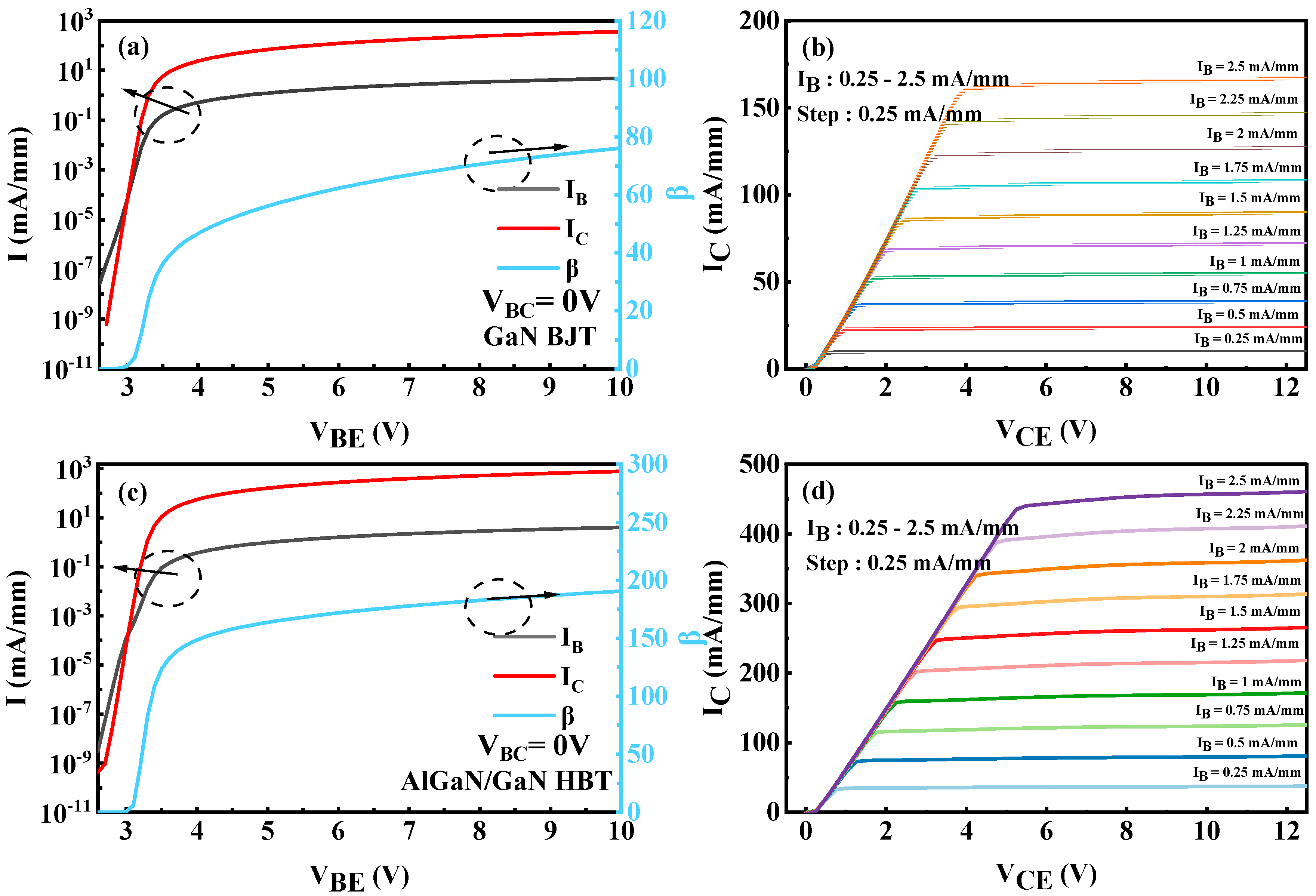
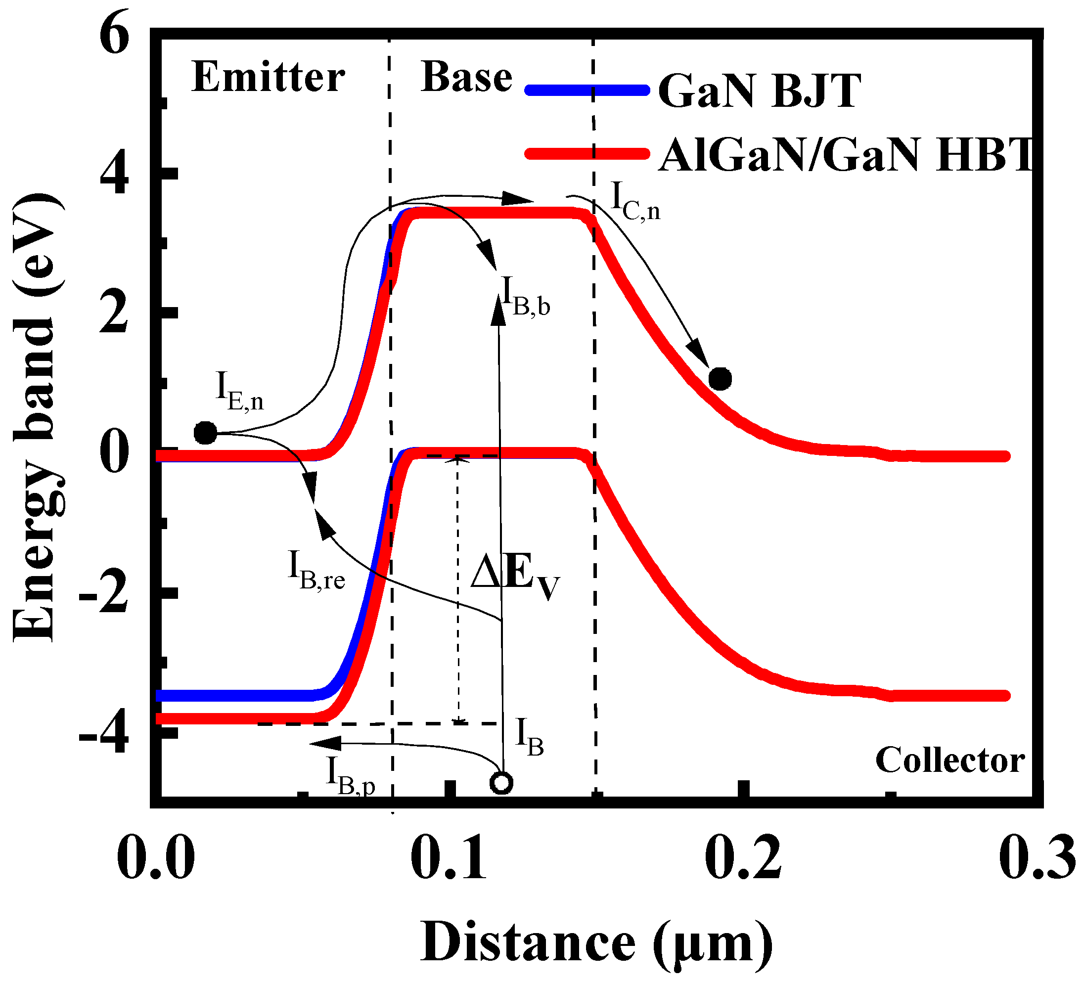
3.1. I–V Characteristics of GaN BJT and AlGaN/GaN HBT

The bipolar junction transistor is an essential semiconductor device characterized by its primary function of current amplification. Composed of two back-to-back PN junctions, the BJT has three main parts: the emitter, the base, and the collector. The heterojunction bipolar transistor, which is a modified form of the BJT, is formed by utilizing different semiconductor materials to create a heterojunction between the emitter and the base. In this section, we focus on the effects of the current gain by employing GaN or AlGaN as the emitter. The stack structures of the GaN BJT and AlGaN/GaN HBT are designed on the drain side of the p-FETs as shown in the circled region in Figure 1a, in order to form the HOB-PFET and the HEB-PFET, respectively. An emitter size of 0.5 × 40 μm2 is possessed by the devices in Figure 2.
Figure 3a shows the Gummel plot of the GaN BJT. The base-collector voltage (VBC) was maintained at a constant 0 V throughout the simulation. The amplification factor (β) is determined by dividing the collector current density ( I C ) by the base current density ( I B ) at various base-emitter voltages (VBE) [27]. The device achieves a current density gain β = 76 at VBE = 10 V with I B = 4.8 mA/mm and I C = 367.7 mA/mm. Figure 3b shows the common-emitter I–V characteristics of the GaN BJT. The collector voltage VCE sweeps from 0 to 12 V, and the base current density IB sweeps from 0.25 to 2.5 mA/mm with 0.25 mA/mm per step. The maximum collector saturation current density is 167.5 mA/mm at VCE = 12 V.
Figure 3c,d are Gummel curves and output curves of AlGaN/GaN HBT. In Figure 3c, the base current density and collector current density intersects at a voltage of 3.2 V. The low crossover voltage indicates a low base resistance [28]. When the base-emitter voltage is 10 V, with a base current density of 4.04 mA/mm and a collector current density of 770.2 mA/mm, the current density gain reaches 191, which is more than 2.5 times larger than the GaN BJT. In addition, the maximum collector saturation current density is as high as 460 mA/mm at VCE = 12 V.
The better current amplification effect shown by AlGaN/GaN HBT can be explained by the energy band diagrams and current composition as shown in Figure 4. The current gain for a BJT amplifier is defined as follow [29]:
β = I C I B = I E , n I B , b I B , r e I B , p + I B , b + I B , r e
The electron diffusion current from the emitter to the base is denoted by I E , n , while the hole diffusion current from the base to the emitter is represented by I B , p . The term I B , r e refers to the complex current within the space charge region of the emitter junction, and I B , b signifies the complex current within the base. I B , b and I B , r e together constitute the current base region of I B . Compared with GaN BJT, the valence band offset ∆EV of the BE junction in AlGaN/GaN HBT is larger due to the band discontinuity between AlGaN/GaN, which further inhibits the reverse injection current of holes from the base region to the emission region I B , p [29], thus improving the injection efficiency. This efficient injection mechanism means that more electrons are able to participate in the amplification process, thereby increasing the gain of the transistor. In addition, the interface of the AlGaN/GaN heterostructure generates a high-density two-dimensional electron gas (2DEG) with higher electron mobility due to the polarization effect, which also contributes to the improvement of current gain.

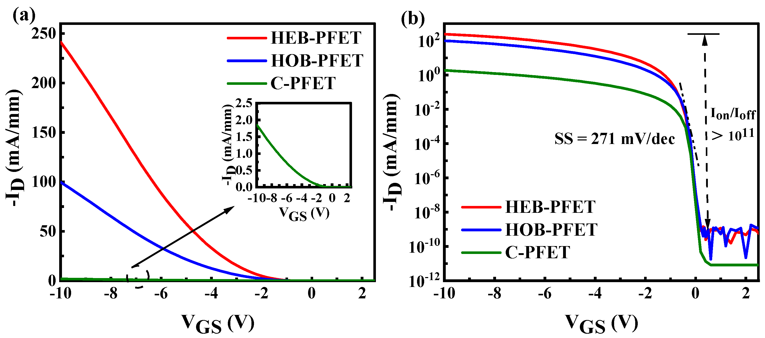
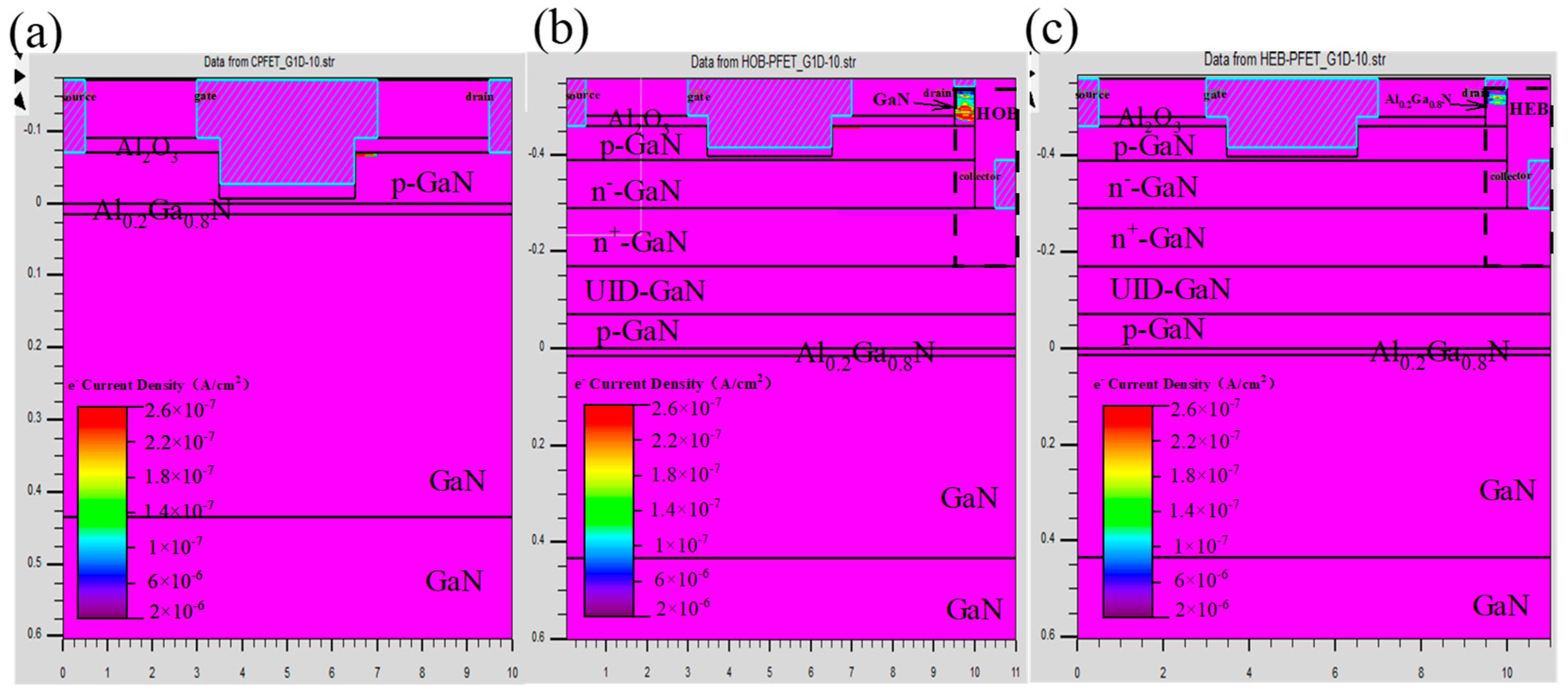
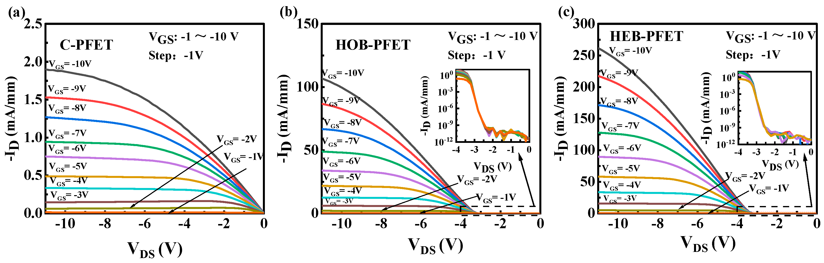
3.2. I–V Characteristics of the C-PFET, HOB-PFET and HEB-PFET

As shown in the circle region in Figure 1a, the GaN BJT or GaN/AlGaN HBT is integrated at the drain side of the conventional p-FET. The contact at the bottom n-GaN layer is shorted with source, defined as Ω side as shown in Figure 1, which is served as an electron source for current amplification [20]. When the device is turned on, the small hole current density in the p-channel is amplified through the BJT to achieve a high current density.
The transfer characteristics in linear and semi-logarithmic coordinates of the C-PFET, HOB-PFET and HEB-PFET are plotted in Figure 5a,b. It can be observed from Figure 5b that the threshold voltages (Vth) of the three structures are −0.83 V, −0.43 V and −0.44 V, respectively, at the current density of 10−2 mA/mm. All the devices reach enhancement mode thanks to the recessed p-GaN gate layer. In addition, the off-state leakage current density of the proposed HEB-PFET is lower than 10−8 mA/mm at VGS = 0 V, offering an ultra-low static power consumption required for CMOS logic circuits [3]. The HEB-PFET has the smallest subthreshold swing (SS) is 271 mV/dec, indicating a faster transition between the on-state and off-state, which is a key factor in achieving high-performance, low-power integrated circuits, where the subthreshold swing of HOB-PFET is 280 mV/dec and C-PFET is 427 mV/dec. The switching conduction ratio (Ion/Ioff) is as high as 1011. As shown in Figure 5b, the off-state current of HEB-PFET and HOB-PFET fluctuated while that of C-PFET did not happen, this can be attributed to the leakage path in npn stack on the drain side. Little electrons exit in the leakage path of the npn stack. Figure 6a–c show the e current density distribution of the C-PFET, HOB-PFET, and HEB-PFET at off-state (@VGS = 1 V, VDS = −10 V), respectively. As can be noticed from Figure 6, compared with C-PFET, a large amount of e- current density can be obviously observed in the npn stack of HOB-PFET and HEB-PFET, resulting in fluctuate off-state leakage current.
Figure 7a–c present output characteristics of the C-PFET, HOB-PFET and HEB-PFET, respectively. Both HOB-PFET and HEB-PFET demonstrate better current conduction capabilities compared with C-PFET. The saturation drain current density of 241 mA/mm is obtained from ID − VD curves of HEB-PFET, while 100 mA/mm and 1.8 mA/mm are achieved for HOB-PFET and C-PFET (@VGS = −10 V, VDS = −10 V), respectively. Therefore, the proposed HEB-PFET exhibits the largest output drain current density of 134 times larger than C-PFET, and 2.4 times larger than HOB-PFET.
There is a detail in the output curves of p-FET with integrated BJT at a small VDS. Compared with the C-PFET, the current density order of HOB-PFET and HEB-PFET is very small within the VDS range of −4–0 V. This distinction can be explained by the VBE0 voltage, identified at the intersection of the IC and IB curves in Figure 3a,c. When VDS < VBE0, BJT is in the cut-off region and blocks the current. Conversely, BJT operates in the amplification region and enhances the current of the p-FET when VDS > VBE0. The inset plot in Figure 7b,c is the output curves of the HEB-PFET in a semi-logarithmic coordinate system across the VDS range from −4 to 0 V, corroborates the above explanation.
Obviously, the HEB-PFET performs the best output characteristics, followed by the HOB-PFET and the C-PFET is the worst. This is due to the fact that the former two integrate npn-type BJT under the drain side, transforming electrons into the primary carriers. Moreover, the HEB-PFET exhibits a higher output current density of 2.4 times larger than HOB-PFET, owing to the larger current density gain of the AlGaN/GaN HBT, which is in consistent with the results in Figure 3. Meanwhile, the gate leakage current density remains at a low level, and the Ion/Ioff ratio does not degrade significantly.

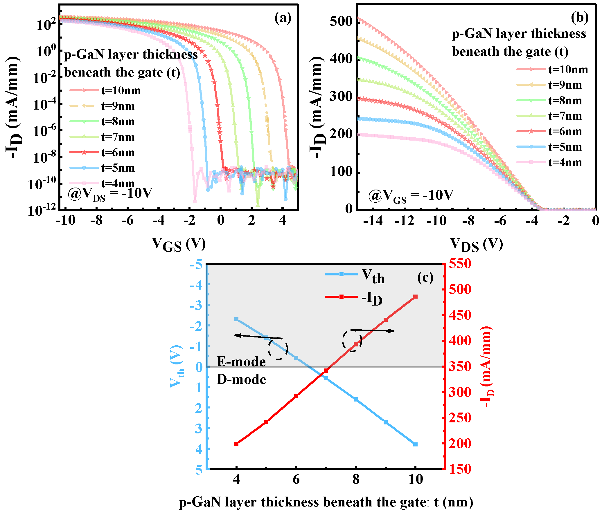
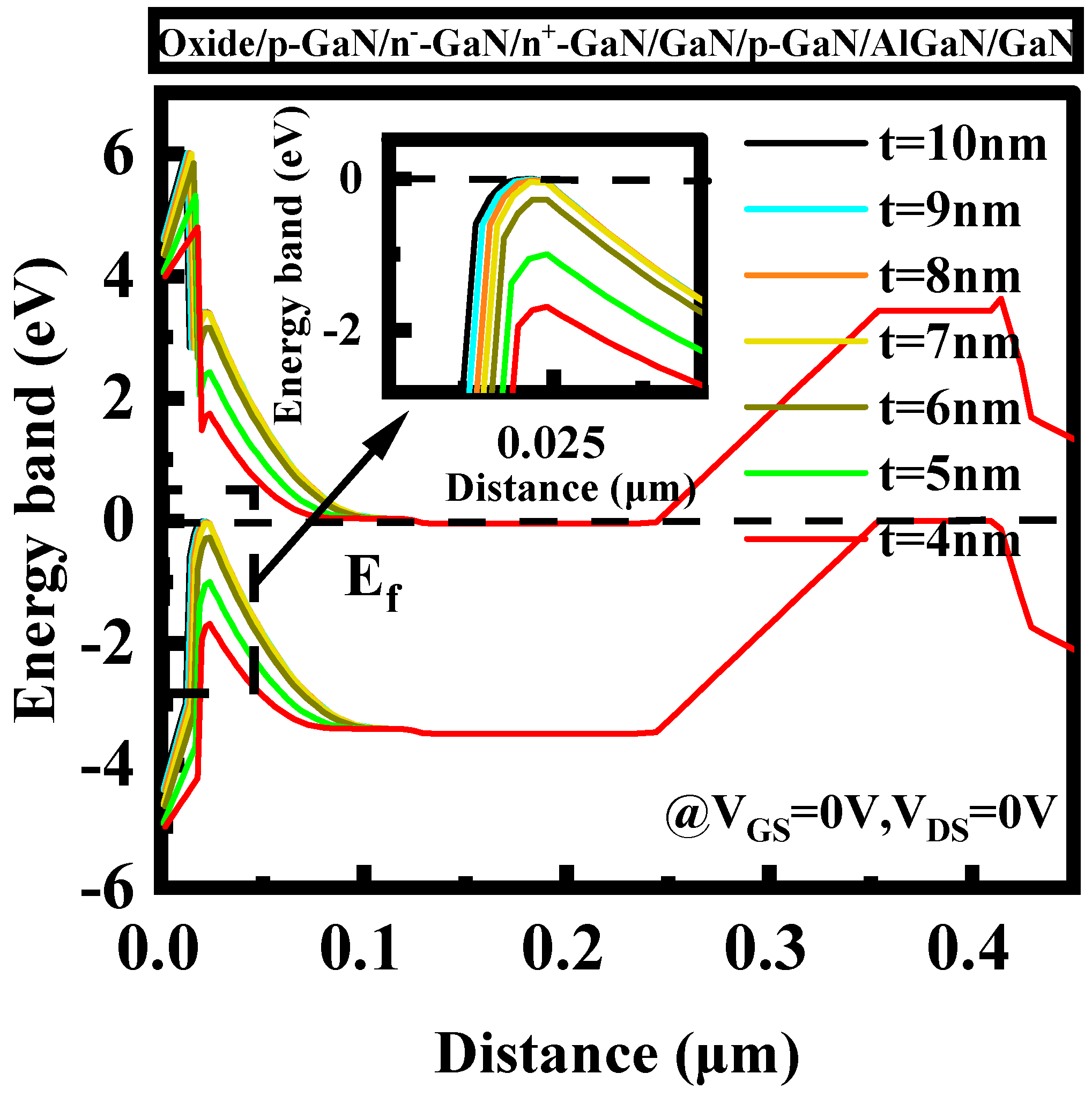
3.3. Optimization of the HEB-PFET

The transfer and output characteristics with the varied t of 4, 5, 6, 7, 8, 9, 10 nm are depicted in Figure 8a,b, respectively. With the reduction in t from 10 to 4 nm, a leftward shift in the transfer curves is observed, resulting in the threshold voltage being transformed from 3.79 V to −2.3 V, and during this process, the output current density drops from 486 mA/mm to 199 mA/mm. In Figure 8c, the threshold gate voltage and drain current density are plotted against different values of t. As the t reduces, the device transitions from depletion mode (D-mode) to E-mode, resulting in a decrease in output current density. The results presented in Figure 8 clearly indicate that the shallow trench sacrifices output current density in exchange for an increased transistor safety threshold. Band diagrams with different values of t are simulated to study the effects of t on Vth shift, as shown in Figure 9. Valence band diagrams in the channel region are under the fermi level at t of 6, 5, and 4 nm, indicating that the hole concentrations in the channel are depleted, resulting in enhancement mode performance. In addition, the downward shift in the valence band with decrement of t, leading to the depletion of holes beneath the gate, thereby shifting the threshold voltage to the left. We carefully balanced the threshold gate voltage and drain current density, ultimately selecting a residual thickness of p-GaN layer of 6 nm beneath the gate with a Vth of −0.44 V, to ensure the device could be turned off efficiently. Simultaneously, a larger drain current density of 241 mA/mm was maintained (@VGS = −10 V, VDS = −10 V).

3.4. Temperature-Dependent Characteristics on the HEB-PFET

The characteristics of the HEB-PFET under different temperature conditions were simulated to understand the thermal stability of the device. Figure 10a presents the temperature-dependent transfer characteristics of the HEB-PFET. Notably, as the temperature increases from 300 K to 425 K, there is a positive shift in the threshold voltage of the HEB-PFET, changing from −0.44 V to −0.21 V. With the temperature transition from 300 K to 425 K, the subthreshold swing changed from 271 mV/dec to 277 mV/dec with little change. As can be noticed from Figure 10b, output current density increases from 30 mA/mm to 49 mA/mm (@VGS = −10 V, VDS = −6 V) with temperature increases from 300 K to 425 K, which is consistent with the phenomenon observed in reference [18]. This increase is likely a result of the enhanced thermal emission of holes [13], which becomes more pronounced at elevated temperatures. Thus, the proposed device exhibits good thermal stability.

3.5. A Semi-Empirical Compact Model for ID of HEB-PFET

In order to further analyze the performance of the HEB-PFET, a semi-empirical compact model is proposed to describe the ID (@|VDS| > VBE0), which combines the current model of the conventional p-FET [30] and the model of the HBT current gain β [29]. The ID of the proposed HEB-PFET is id · β, where id describes the current of the conventional p-FET and β is the current gain of the AlGaN/GaN HBT. The id is defined as follows [30]:
In linear region (VDS > VGS − VTH)
i d = μ p C ox W G L G [ ( V GS V TH ) V DS 1 2 V 2 DS ]
In saturated region (VDS ≤ VGS − VTH)
i d = 1 2 μ p C ox W G L G ( V GS V TH ) 2
In Formulas (2) and (3), μp is the hole mobility, WG and LG are the width and length of the gate, Cox = (εox/tox) is the capacitances across the Al2O3 layers. VTH is the threshold voltage of the conventional p-FET, any further drain-induced threshold shift is accounted for by shifting VTH = VT0 − δVDS from its low-bias value VT0 [8].
In addition, β is given below:
β = N E t E N B t B · D nB D pE · a · 1 + n exp ( V DS V 0 k ) 1 + exp ( V DS V 0 k )
The thickness and concentration of the p-GaN and Al0.2Ga0.8N layer under the drain are denoted as tB, tE, NB and NE, respectively. DpE and DnB are the diffusion coefficients of holes and electrons in the Al0.2Ga0.8N layer under the drain and p-GaN. V0 is considered to be the voltage threshold that marks the beginning of transistor amplification. The a, n, and k are all constants related to VGS.
The basic part of the model, id is a formula widely used to describe the current behavior of conventional p-FETs in different operating regions (linear region and saturated region) [30]. Then, the second part of the model, β describes the current gain effect due to the integrated AlGaN/GaN HBT at the drain side. The parameters a, n and k are introduced to characterize the electrical behavior of the HBT, which are dependent on the variation of VGS, reflecting the amplification effects of the triode at different gate source voltages.
Figure 11 presents the fitting diagram between the predicted values of the model and the simulated values. The model, which combines the current model of the conventional p-FET and the model of the HBT current gain β, intuitively explains the working principle of HEB-PFET. It not only provides a powerful tool for predicting and optimizing the electrical characteristics of the HEB-PFET, but also offers new perspectives and ideas for the design of GaN p-FET devices.

4. Conclusions

In summary, a novel e-mode HEB-PFET structure is demonstrated to advance the state-of-the-art for GaN p-FETs in current level. The simulation results indicate that the integration of a AlGaN/GaN HBT can amplify current density by a factor of 134 and 2.4 compared with C-PFET and HOB-PFET, respectively. The optimized HEB-PFET with 6 nm p-GaN layer underneath the gate exhibits 241 mA/mm drain current density, with Vth of −0.44 V and Ion/Ioff of >1011. Additionally, the proposed HEB-PFET shows a good thermal stability when the temperature changes from 300 K to 425 K, where the Vth shows a 0.23 V increase, the subthreshold voltage shows only a 6 mV/dec increment, and the output current density shows a 19 mA/mm increase. A semi-empirical compact model is proposed to predict the current characteristics of the devices. Therefore, the HEB-PFET is a very attractive device that can be integrated with commercial p-GaN gate HEMT to form GaN based CMOS. Future research will concentrate on fabricating the proposed device, with a focus on the growth of GaN/AlGaN heterostructure with high concentration of holes, minimizing etching damage, and optimization of ohmic contact of source side.

Author Contributions

Conceptualization, M.G.; software, W.Z. and S.T.; data curation, Y.L.; writing—original draft preparation, W.Z.; writing—review and editing, C.Y. and D.C. All authors have read and agreed to the published version of the manuscript.

Funding

This work was supported in part by the National Natural Science Foundation of China under Grant 62004109, Grant 62074085, Grant 61874168 and Grant 62074087, and the Natural Science Research of Jiangsu Higher Education Institutions of China under Grant 24KJB510037.

Data Availability Statement

Date are contained within the article.

Conflicts of Interest

The authors declare no conflicts of interest.

References

  1. Chen, K.J.; Häberlen, O.; Lidow, A.; Tsai, C.L.; Ueda, T.; Uemoto, Y.; Wu, Y. GaN-on-Si power technology: Devices and applications. IEEE Trans. Electron Devices 2017, 64, 779–795. [Google Scholar] [CrossRef]
  2. Zheng, Z.; Song, E.; Zhang, L.; Yang, S.; Xu, H.; Wong, R.K.-Y.; Wei, J.; Chen, K.J. Enhancement-Mode GaN p-Channel MOSFETs for Power Integration. In Proceedings of the 2020 32nd International Symposium on Power Semiconductor Devices and ICs (ISPSD), Vienna, Austria, 13–18 September 2020. [Google Scholar]
  3. Chen, K.; Su, Y.; Ruan, J.; Cai, Y.; Zhu, L.; Zhang, B.; Zhou, Q. A novel E-mode GaN p-MOSFET featuring charge storage layer with high current density. J. Phys. D Appl. Phys. 2022, 55, 444007. [Google Scholar] [CrossRef]
  4. Chen, J.; Liu, Z.; Wang, H.; He, Y.; Zhu, X.; Ning, J.; Zhang, J.; Hao, Y. A GaN Complementary FET Inverter With Excellent Noise Margins Monolithically Integrated With Power Gate-Injection HEMTs. IEEE Trans. Electron Devices 2022, 69, 51–56. [Google Scholar] [CrossRef]
  5. Chen, F.; Qin, G.; Li, L.; Zhai, J.; Chen, Y. Simulation of E-mode p-channel GaN/AlGaN HFETs with hybrid AlGaN barrier layer. In Proceedings of the 2023 Cross Strait Radio Science and Wireless Technology Conference (CSRSWTC), Guilin, China, 10–13 November 2023. [Google Scholar]
  6. Nakajima, A.; Liu, P.; Ogura, M.; Makino, T.; Kakushima, K.; Nishizawa, S.-I.; Ohashi, H.; Yamasaki, S.; Iwai, H. Generation and transportation mechanisms for two-dimensional hole gases in GaN/AlGaN/GaN double heterostructures. J. Appl. Phys. 2014, 115, 153707. [Google Scholar] [CrossRef]
  7. Chowdhury, N.; Lemettinen, J.; Xie, Q.; Zhang, Y.; Rajput, N.S.; Xiang, P.; Cheng, K.; Suihkonen, S.; Then, H.W.; Palacios, T. p-Channel GaN Transistor Based on p-GaN/AlGaN/GaN on Si. IEEE Trans. Electron Devices 2019, 40, 1036–1039. [Google Scholar] [CrossRef]
  8. Bader, S.J.; Chaudhuri, R.; Nomoto, K.; Hickman, A.; Chen, Z.; Then, H.W.; Muller, D.A.; Xing, H.G.; Jena, D. Gate-recessed E-mode p-channel HFET with high on-current based on GaN/AlN 2D hole gas. IEEE Electron Device Lett. 2018, 39, 1848–1851. [Google Scholar] [CrossRef]
  9. Nomoto, K.; Chaudhuri, R.; Bader, S.J.; Li, L.; Hickman, A.; Huang, S.; Lee, H.; Maeda, T.; Then, H.W.; Radosavljevic, M.; et al. GaN/AlN p-channel HFETs with Imax > 420 mA/mm and ~20 GHz fT/fMAX. In Proceedings of the 2020 IEEE International Electron Devices Meeting (IEDM), San Francisco, CA, USA, 12–18 December 2020. [Google Scholar]
  10. Zimmermann, T.; Neuburger, M.; Kunze, M.; Daumiller, I.; Denisenko, A.; Dadgar, A.; Krost, A.; Kohn, E. P-channel InGaN-HFET structure based on polarization doping. IEEE Electron Device Lett. 2004, 25, 450–452. [Google Scholar] [CrossRef]
  11. Reuters, B.; Hahn, H.; Pooth, A.; Holländer, B.; Breuer, U.; Heuken, M.; Kalisch, H.; Vescan, A. Fabrication of p-channel heterostructure field effect transistors with polarization-induced two-dimensional hole gases at metal–polar GaN/AlInGaN interfaces. J. Phys. D Appl. Phys. 2014, 47, 175103. [Google Scholar] [CrossRef]
  12. Hahn, H.; Reuters, B.; Pooth, A.; Hollander, B.; Heuken, M.; Kalisch, H.; Vescan, A. p-Channel Enhancement and Depletion Mode GaN-Based HFETs With Quaternary Backbarriers. IEEE Trans. Electron Devices 2013, 60, 3005–3011. [Google Scholar] [CrossRef]
  13. Su, H.; Zhang, T.; Xu, S.; Tao, H.; Gao, Y.; Liu, X.; Xie, L.; Xiang, P.; Cheng, K.; Hao, Y.; et al. An energy-band modulated p-GaN/InGaN/AlN p-channel MESFET with high ION/IOFF ratio and steep subthreshold swing. Appl. Phys. Lett. 2024, 124, 162102. [Google Scholar] [CrossRef]
  14. Xing, Z.; Zhang, H.; Ye, Y.; Liang, F.; Yang, L.; Huang, Z.; Liang, K.; Wang, H.; Zhang, M.; Li, J.; et al. GaN-based E-mode p-FETs with polarization-doped p-type graded AlGaN channels. J. Phys. D Appl. Phys. 2024, 57, 385102. [Google Scholar] [CrossRef]
  15. Zheng, Z.; Song, W.; Zhang, L.; Yang, S.; Wei, J.; Chen, K.J. High ION and ION/IOFF Ratio Enhancement-Mode Buried p-Channel GaN MOSFETs on p-GaN Gate Power HEMT Platform. IEEE Electron Device Lett. 2020, 41, 26–29. [Google Scholar] [CrossRef]
  16. Chen, F.; Hao, R.; Yu, G.; Zhang, X.; Song, L.; Wang, J.; Cai, Y.; Zhang, B. Enhancement-mode n-GaN gate p-channel heterostructure field effect transistors based on GaN/AlGaN 2D hole gas. Appl. Phys. Lett. 2019, 115, 112103. [Google Scholar] [CrossRef]
  17. Kumar, A.; De Souza, M.M. Extending the bounds of performance in E-mode pchannel GaN MOSHFETs. In Proceedings of the 2016 IEEE International Electron Devices Meeting (IEDM), San Francisco, CA, USA, 3–7 December 2016. [Google Scholar]
  18. Yang, C.; Fu, H.; Peri, P.; Fu, K.; Zhou, J.; Montes, J.; Smith, D.J.; Zhao, Y. Enhancement-mode gate-recess-free gan-based p-channel heterojunction field-effect transistor with ultra-low subthreshold swing. IEEE Electron Device Lett. 2021, 42, 1128–1131. [Google Scholar] [CrossRef]
  19. Raj, A.; Krishna, A.; Romanczyk, B.; Keller, S.; Mishra, U.K. GaN/AlGaN Superlattice Based E-Mode Hole Channel FinFET With Schottky Gate. IEEE Electron Device Lett. 2023, 44, 9–12. [Google Scholar] [CrossRef]
  20. Tang, J.; Jiang, Z.; Wang, C.; Chen, J.; Chen, H.; Zhang, Y.; Zheng, Z.; Wang, X.; Ma, J.; Zhao, J.; et al. Bipolar p-FET with Enhanced Conduction Capability on E-mode GaN-on-Si HEMT Platform. In Proceedings of the 2023 International Electron Devices Meeting (IEDM), San Francisco, CA, USA, 9–13 December 2023. [Google Scholar]
  21. Zhou, J.; Do, H.-B.; De Souza, M.M. Impact of an Underlying 2DEG on the Performance of a p-Channel MOSFET in GaN. ACS Appl. Electron. Mater. 2023, 5, 3309–3315. [Google Scholar] [CrossRef]
  22. ‘Silvaco TCAD Atlas’, Version V3.44.1R. 2017. Available online: https://www.silvaco.com/products/tcad.html (accessed on 24 November 2017).
  23. Kumar, A.; De Souza, M.M. Modelling the threshold voltage of p-channel enhancement-mode GaN heterostructure field-effect transistors. IET Power Electron. 2018, 11, 675–680. [Google Scholar] [CrossRef]
  24. Albrecht, J.D.; Wang, R.P.; Ruden, P.P.; Farahmand, M.; Brennant, K.F. Electron transport characteristics of GaN for high temperature device modeling. J. Appl. Phys. 1998, 83, 4777–4781. [Google Scholar] [CrossRef]
  25. Wang, W.; Shervin, S.; Oh, S.K.; Chen, J.; Huai, Y.; Pouladi, S.; Kim, H.; Lee, S.-N.; Ryou, J.-H. Flexible AlGaInN/GaN Heterostructures for High-Hole-Mobility Transistors. IEEE Electron Device Lett. 2017, 38, 1086–1089. [Google Scholar] [CrossRef]
  26. Yan, S.; Zhou, Y.; Liu, J.; Zhong, Y.; Sun, X.; Chen, X.; Guo, X.; Li, Q.; Sun, Q.; Yang, H. GaN-Based Double-Heterojunction Bipolar Transistors with a Composition Graded p-InGaN Base. IEEE Trans. Electron Devices 2023, 70, 1613–1621. [Google Scholar] [CrossRef]
  27. Kumabe, T.; Watanabe, H.; Ando, Y.; Tanaka, A.; Nitta, S.; Honda, Y.; Amano, H. ‘Regrown-free’ fabrication of high-current-gain AlGaN/GaN heterojunctio bipolat transistor with N-p-n configuration. Appl. Phys. Exp. 2022, 15, 046506. [Google Scholar] [CrossRef]
  28. Zhang, L.; Wang, X.; Zeng, J.; Jia, L.; Cheng, Z.; Ai, Y.; Liu, Z.; Tan, W.; Zhang, Y. AlGaN/GaN Heterojunction Bipolar Transistors with High Current Gain and Low Specific ON-Resistance. IEEE Trans. Electron Devices 2022, 69, 6633–6636. [Google Scholar] [CrossRef]
  29. Wang, X.; Zhang, L.; He, J.; Cheng, Z.; Liu, Z.; Zhang, Y. Simulation and Comprehensive Analysis of AlGaN/GaN HBT for High Voltage and High Current. Electronics 2023, 12, 3590. [Google Scholar] [CrossRef]
  30. Van Zeghbroeck, B. Principles of Semiconductor Devices; Colarado University: Boulder, CO, USA, 2011. [Google Scholar]
Figure 1. Schematic cross section of (a) the HEB-PFET proposed in this work (t is p-GaN layer thickness underneath the gate), (b) p-GaN HEMT platform and (c) the conventional p-FET (C-PFET). (d) Verification of the simulation models with ID − VGS characteristics [5] of p-FET in Silvaco TCAD.
Electronics 13 04752 g001
Figure 2. Schematic of (a) the GaN BJT and (b) the AlGaN/GaN HBT. (Device dimensions: LE/LB/LC/WE/LEB/LBC/LEC = 0.5 μm/0.5 μm/0.5 μm/40 μm/9 μm/10 μm/0.5 μm).
Electronics 13 04752 g002
Figure 3. (a) The simulated Gummel plots of GaN BJT with AE = 0.5 × 40 μm2. (b) Common-emitter I–V characteristics of GaN BJT. Common-emitter (c) transfer and (d) output characteristics curves of AlGaN/GaN HBT.
Electronics 13 04752 g003
Figure 4. Energy band diagrams of the GaN BJT and the AlGaN/GaN HBT (@VGS = 0 V, VDS = 0 V).
Electronics 13 04752 g004
Figure 5. (a) Linear-scale (Inset: a magnification plot of transfer curves of the C-PFET) and (b) Semilog-scale transfer curves of the C-PFET, HOB-PFET and HEB-PFET. (@VDS = −10 V).
Electronics 13 04752 g005
Figure 6. The e current density distribution of the (a) C-PFET, (b) HOB-PFET, and (c) HEB-PFET at off-state (@VGS = 1 V, VDS = −10 V), respectively.
Electronics 13 04752 g006
Figure 7. Output characteristics of (a) C-PFET, (b) HOB-PFET and (c) HEB-PFET. Inset plots in (b,c) are the output curves in a semilog-scale over the VDS range of −4–0 V.
Electronics 13 04752 g007
Figure 8. (a) ID − VGS curves in semilog-scale and (b) ID − VDS curves of the HEB-PFET with the variation in t. (c) Vth and ID as a function of t.
Electronics 13 04752 g008
Figure 9. Energy band diagrams of the HEB-PFET with the variation in t. (@VGS = 0 V, VDS = 0 V) Inset: a magnification plot of valence band of the HEB-PFET in the channel region.
Electronics 13 04752 g009
Figure 10. Temperature-dependent. (a) transfer (@VDS = −5 V) and (b) output curves (@VGS = −10 V) of the HEB-PFET from 300 K to 425 K.
Electronics 13 04752 g010
Figure 11. Compact model (thin red) fitted to simulation data (black circles).
Electronics 13 04752 g011
Disclaimer/Publisher’s Note: The statements, opinions and data contained in all publications are solely those of the individual author(s) and contributor(s) and not of MDPI and/or the editor(s). MDPI and/or the editor(s) disclaim responsibility for any injury to people or property resulting from any ideas, methods, instructions or products referred to in the content.

