
Spin Current Enhancement Using Double-Ferromagnetic-Layer Structure for Magnetoelectric Spin-Orbit Logic Device


Abstract
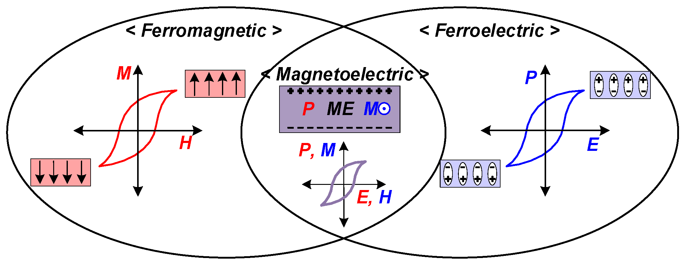
1. Introduction
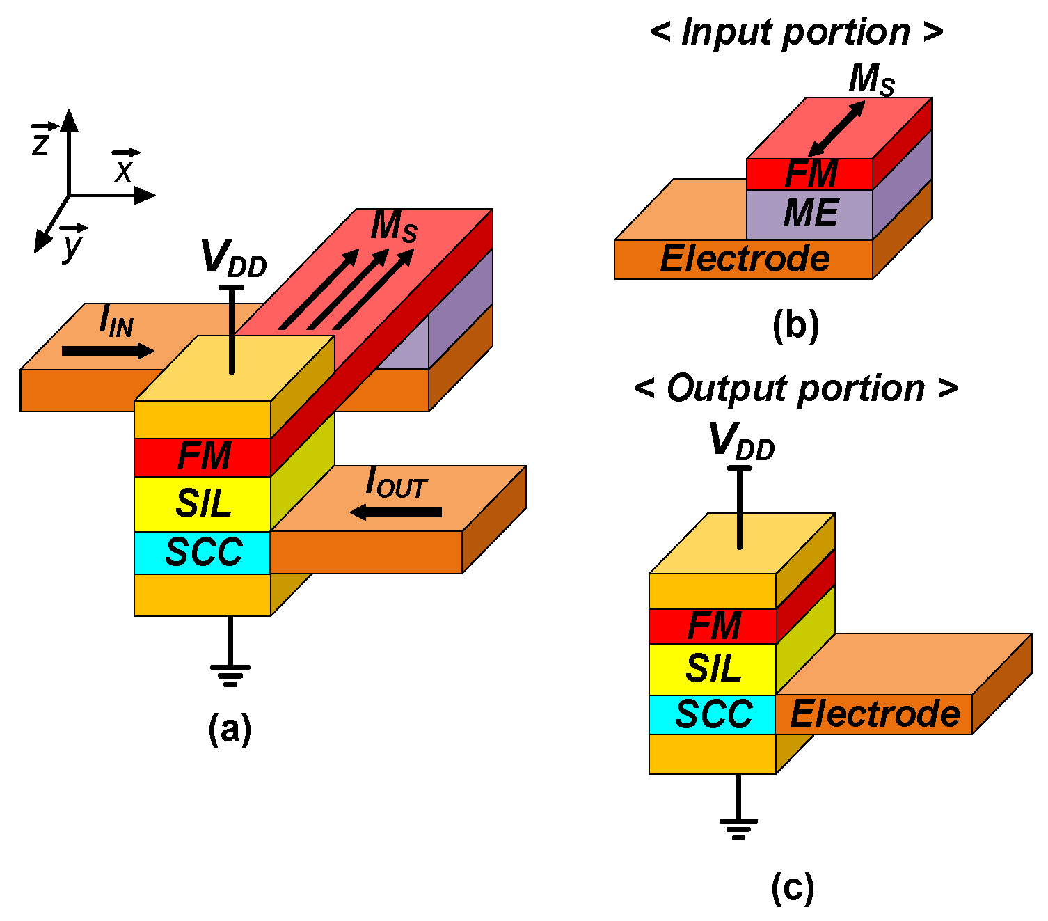
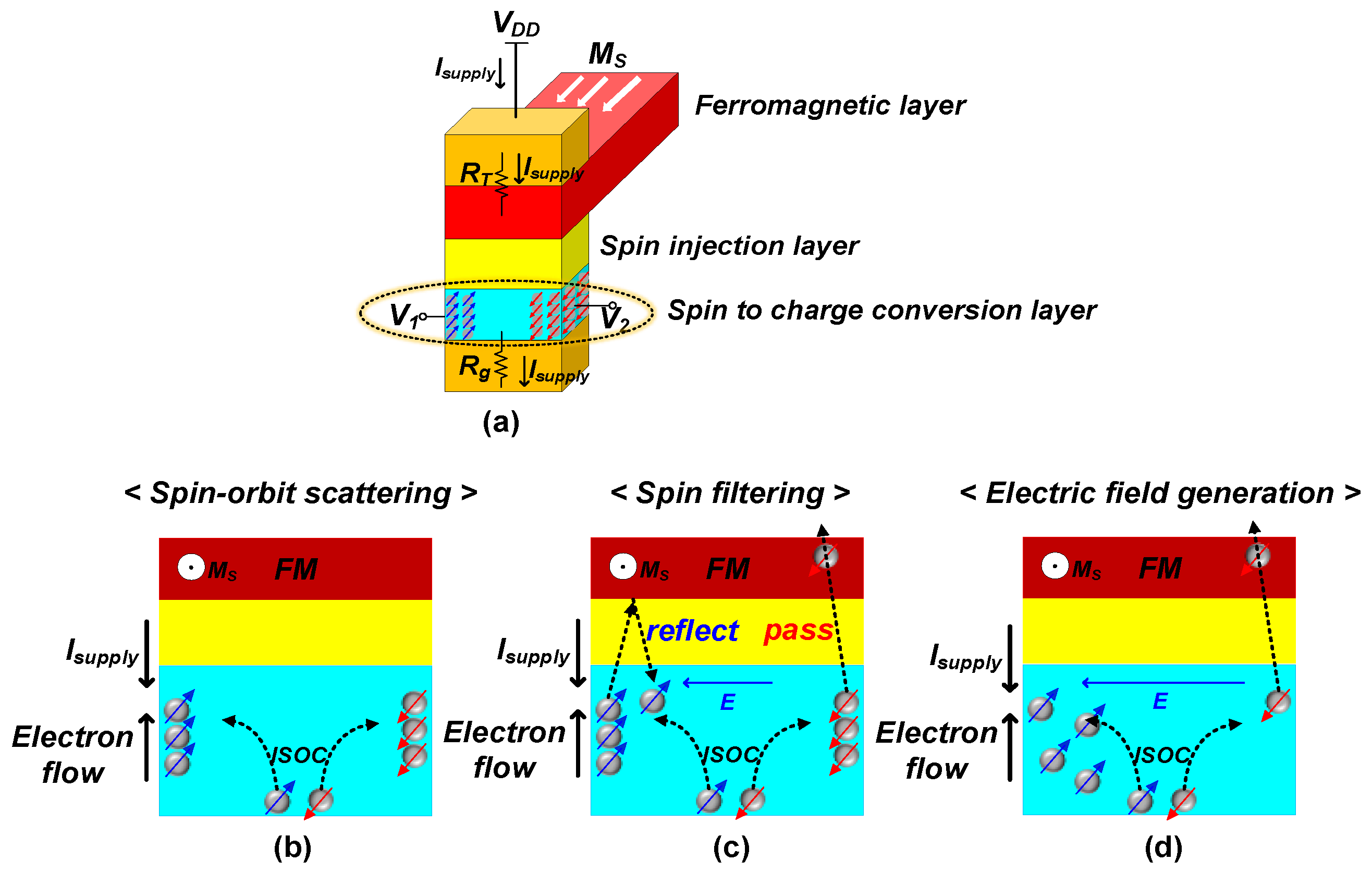
2. Review of the Existing Structure
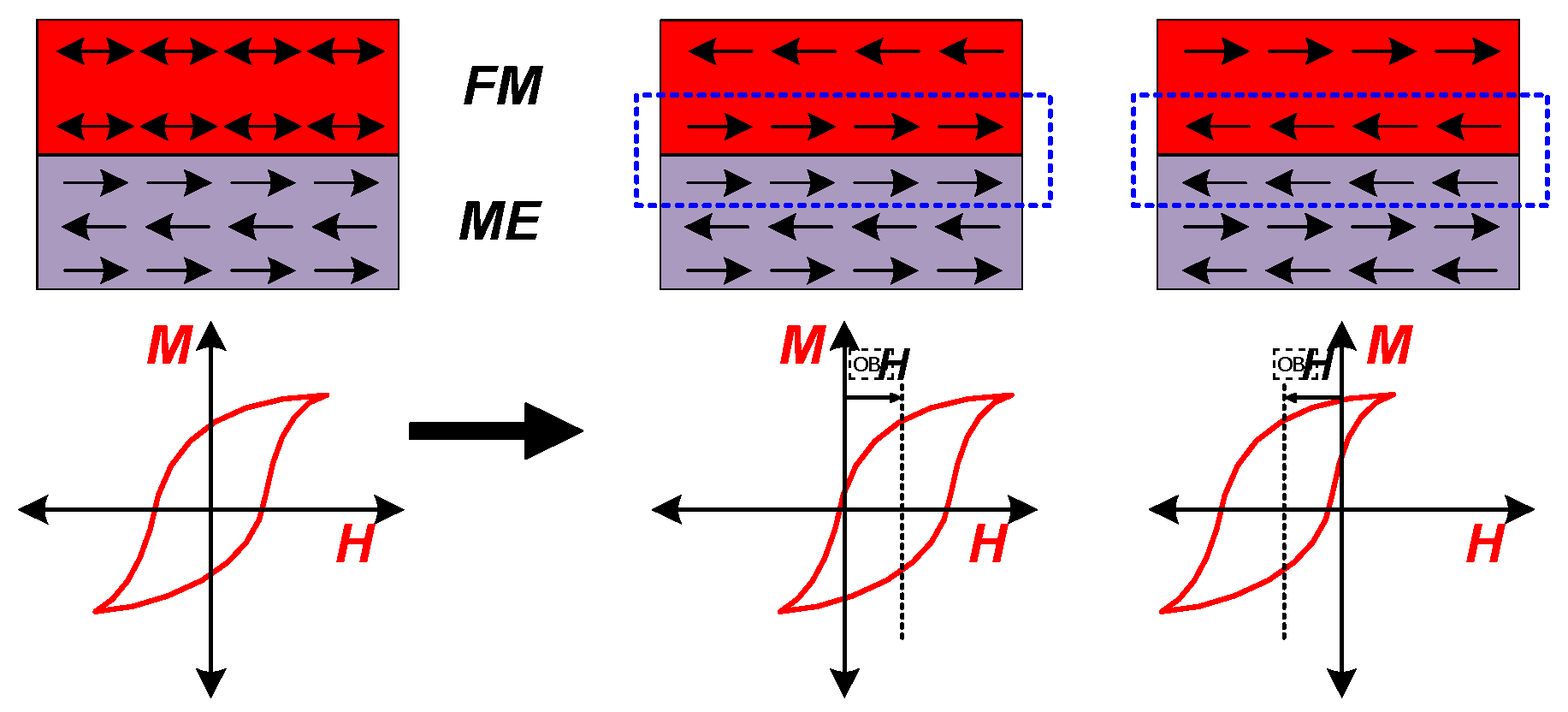
2.1. Operating Mechanism of the Input Portion of MESO
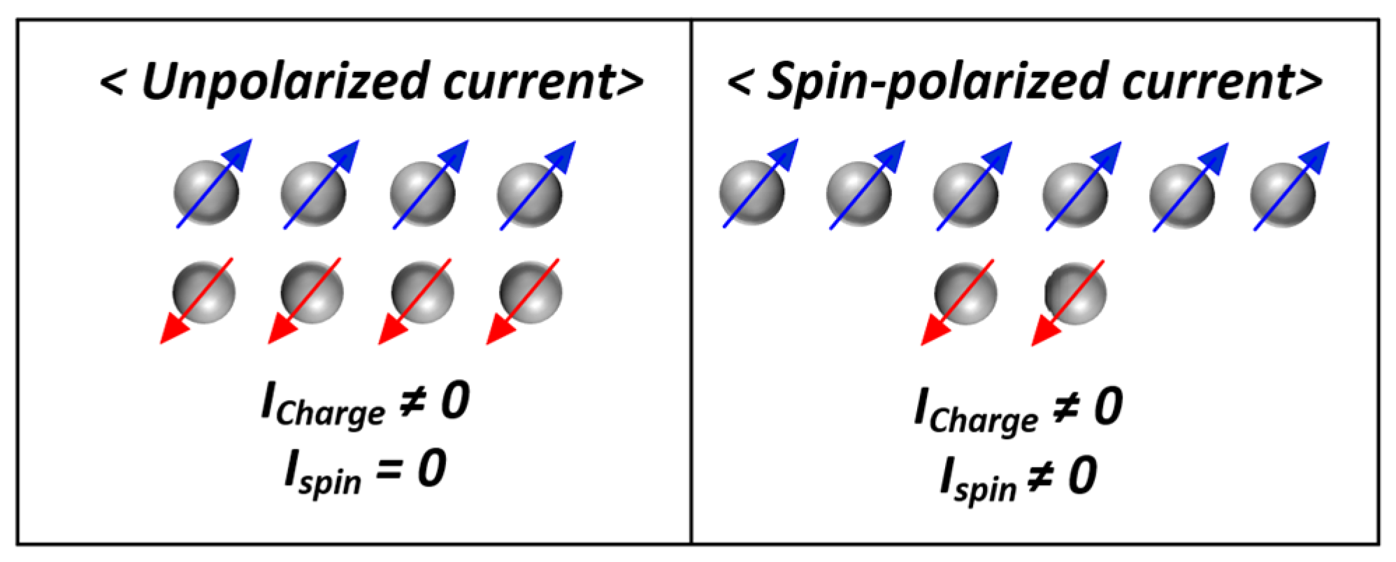
2.2. Operating Mechanism of the Output Portion of MESO
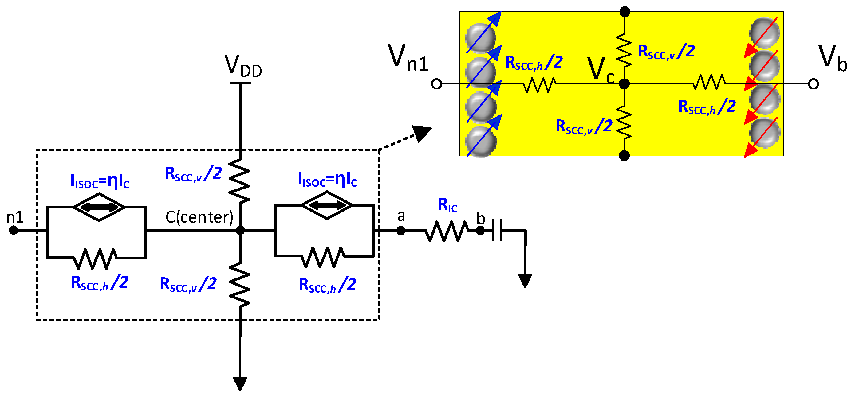
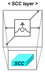
2.3. Circuit Modeling
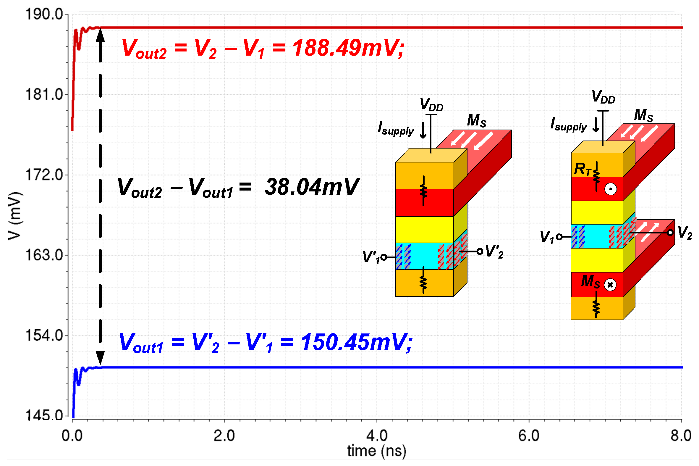
3. Double-FM-Layer Structure for MESO Device
4. Simulation Results
5. Conclusions
Author Contributions
Funding
Data Availability Statement
Acknowledgments
Conflicts of Interest
References
- Powell, J.R. The Quantum Limit to Moore’s Law. Proc. IEEE 2008, 96, 1247–1248. [Google Scholar] [CrossRef]
- Nikonov, D.E.; Young, I.A. Overview of Beyond-CMOS Devices and a Uniform Methodology for Their Benchmarking. Proc. IEEE 2013, 101, 2498–2533. [Google Scholar] [CrossRef]
- Theis, T.N.; Solomon, P.M. It’s Time to Reinvent the Transistor! Science 2010, 327, 1600–1601. [Google Scholar] [CrossRef]
- Nikonov, D.E.; Young, I.A. Benchmarking of Beyond-CMOS Exploratory Devices for Logic Integrated Circuits. IEEE J. Explor. Solid-State Comput. Devices Circuits 2015, 1, 3–11. [Google Scholar] [CrossRef]
- Manipatruni, S.; Nikonov, D.E.; Lin, C.-C.; Gosavi, T.A.; Liu, H.; Prasad, B.; Huang, Y.-L.; Bonturim, E.; Ramesh, R.; Young, I.A. Scalable energy-efficient magnetoelectric spin–orbit logic. Nature 2019, 565, 35–42. [Google Scholar] [CrossRef]
- Seabaugh, A.C.; Zhang, Q. Low-Voltage Tunnel Transistors for Beyond CMOS Logic. Proc. IEEE 2010, 98, 2095–2110. [Google Scholar] [CrossRef]
- Rojas-Sánchez, J.-C.; Oyarzún, S.; Fu, Y.; Marty, A.; Vergnaud, C.; Gambarelli, S.; Vila, L.; Jamet, M.; Ohtsubo, Y.; Taleb-Ibrahimi, A.; et al. Spin to charge conversion at room temperature by spin pumping into a new type of topological insulator: α-Sn films. Phys. Rev. Lett. 2016, 116, 096602. [Google Scholar] [CrossRef]
- Sinova, J.; Valenzuela, S.O.; Wunderlich, J.; Back, C.H.; Jungwirth, T. Spin hall effects. Rev. Mod. Phys. 2015, 87, 1213. [Google Scholar] [CrossRef]
- Rojas-Sánchez, J.C.; Reyren, N.; Laczkowski, P.; Savero, W.; Attané, J.P.; Deranlot, C.; Jaffrès, H. Spin pumping and inverse spin Hall efect in platinum: Te essential role of spin-memory loss at metallic interfaces. Phys. Rev. Lett. 2014, 112, 106602. [Google Scholar] [CrossRef]
- Zhang, S.; Fert, A. Conversion between spin and charge currents with topological insulators. Phys. Rev. B 2016, 94, 184423. [Google Scholar] [CrossRef]
- Li, C.; Cai, L.; Wang, S.; Yang, X.; Cui, H.; Wei, B.; Liu, B. Performance Optimization of All-Spin Logic Device Based on Silver Interconnects and Asymmetric Tunneling Layer. IEEE Trans. Magn. 2018, 54, 1–6. [Google Scholar] [CrossRef]
- Liang, Z.; Mankalale, M.G.; Hu, J.; Zhao, Z.; Wang, J.-P.; Sapatnekar, S.S. Performance Characterization and Majority Gate Design for MESO-Based Circuits. IEEE J. Explor. Solid-State Comput. Devices Circuits 2018, 4, 51–59. [Google Scholar] [CrossRef]
- Liu, H.; Manipatruni, S.; Morris, D.H.; Vaidyanathan, K.; Nikonov, D.E.; Karnik, T.; Young, I.A. Synchronous Circuit Design With Beyond-CMOS Magnetoelectric Spin–Orbit Devices Toward 100-mV Logic. IEEE J. Explor. Solid-State Comput. Devices Circuits 2019, 5, 1–9. [Google Scholar] [CrossRef]
- Li, H.; Lin, C.-C.; Nikonov, D.E.; Young, I.A. Differential Electrically Insulated Magnetoelectric Spin-Orbit Logic Circuits. IEEE J. Explor. Solid-State Comput. Devices Circuits 2021, 7, 18–28. [Google Scholar] [CrossRef]
- Liang, X.; Chen, H.; Sun, N.X. Magnetoelectric materials and devices. APL Mater. 2021, 9, 041114. [Google Scholar] [CrossRef]
- Cherifi, R.O.; Ivanovskaya, V.; Phillips, L.C.; Zobelli, A.; Infante, I.C.; Jacquet, E.; Garcia, V.; Fusil, S.; Briddon, P.R.; Guiblin, N.; et al. Electric-field control of magnetic order above room temperature. Nat. Mater. 2014, 13, 345–351. [Google Scholar] [CrossRef]
- Ohno, H.; Chiba, D.; Matsukura, F.; Omiya, T.; Abe, E.; Dietl, T.; Ohno, Y.; Ohtani, K. Electric-field control of ferromagnetism. Nature 2000, 408, 944–946. [Google Scholar] [CrossRef]
- Manipatruni, S.; Nikonov, D.E.; Lin, C.-C.; Prasad, B.; Huang, Y.-L.; Damodaran, A.R.; Chen, Z.; Ramesh, R.; Young, I.A. Voltage control of unidirectional anisotropy in ferromagnet-multiferroic system. Sci. Adv. 2018, 4, eaat4229. [Google Scholar] [CrossRef]
- Manipatruni, S.; Nikonov, D.E.; Ramesh, R.; Li, H.; Young, I.A. Spin-Orbit Logic With Magnetoelectric Nodes: A Scalable Charge Mediated Nonvolatile Spintronic Logic. 2017. Available online: https://arxiv.org/abs/1512.05428v2 (accessed on 18 May 2024).
- Mazin, I.I. How to define and calculate the degree of spin polarization in ferromagnets. Phys. Rev. Lett. 1999, 83, 1427–1430. [Google Scholar] [CrossRef]
- Kumar, A.; Fulara, H.; Khymyn, R.; Litvinenko, A.; Zahedinejad, M.; Rajabali, M.; Zhao, X.; Behera, N.; Houshang, A.; Awad, A.A.; et al. Robust Mutual Synchronization in Long Spin Hall Nano-oscillator Chains. Nano Lett. 2023, 23, 6720–6726. [Google Scholar] [CrossRef]
- Ren, H.; Zheng, X.Y.; Channa, S.; Wu, G.; O’mahoney, D.A.; Suzuki, Y.; Kent, A.D. Hybrid spin Hall nano-oscillators based on ferromagnetic metal/ferrimagnetic insulator heterostructures. Nat. Commun. 2023, 14, 1406. [Google Scholar] [CrossRef]
- Zhang, Z.; Zheng, Z.; Zhang, Y.; Sun, J.; Lin, K.; Zhang, K.; Feng, X.; Chen, L.; Wang, J.; Wang, G.; et al. 3D Ferrimagnetic Device for Multi-Bit Storage and Efficient In-Memory Computing. IEEE Electron Device Lett. 2021, 42, 152–155. [Google Scholar] [CrossRef]
- Kim, S.K.; Beach, G.S.D.; Lee, K.-J.; Ono, T.; Rasing, T.; Yang, H. Ferrimagnetic spintronics. Nat. Mater. 2022, 21, 24–34. [Google Scholar] [CrossRef]
- Chowdhury, N.; Khan, K.I.A.; Bangar, H.; Gupta, P.; Yadav, R.S.; Agarwal, R.; Kumar, A.; Muduli, P.K. Kagome Magnets: The Emerging Materials for Spintronic Memories. Proc. Natl. Acad. Sci. India Sect. A Phys. Sci. 2023, 93, 477–495. [Google Scholar] [CrossRef]
- Cheng, E.; Yan, L.; Shi, X.; Lou, R.; Fedorov, A.; Behnami, M.; Yuan, J.; Yang, P.; Wang, B.; Cheng, J.-G.; et al. Tunable positions of Weyl nodes via magnetism and pressure in the ferromagnetic Weyl semimetal CeAlSi. Nat. Commun. 2024, 15, 1467. [Google Scholar] [CrossRef]
- Itoh, S.; Endoh, Y.; Yokoo, T.; Ibuka, S.; Park, J.-G.; Kaneko, Y.; Takahashi, K.S.; Tokura, Y.; Nagaosa, N. Weyl fermions and spin dynamics of metallic ferromagnet SrRuO3. Nat. Commun. 2016, 7, 11788. [Google Scholar] [CrossRef]
- Hong, S.; Sayed, S.; Datta, S. Spin Circuit Representation for the Spin Hall Effect. IEEE Trans. Nanotechnol. 2016, 15, 225–236. [Google Scholar] [CrossRef]


| Symbol | Description | Value |
|---|---|---|
 | Saturation magnetization | 1.0 × 10⁶ A/m |
| Demagnetizing factors | (0, 0, 0.8) | |
| Damping constant | 0.007 | |
| In-plane anisotropy | 0 | |
| Polarization efficiency | 0.8 | |
| Field-like torque coefficient | 0 | |
| VCMA coefficient | 60 fj/V·m | |
| Initial state (±1) | +1 for FM 1 and −1 for FM 2 | |
| Magnet thickness | 1 nm | |
| Magnet width | 20 nm | |
| Magnet length | 40 nm | |
| Spin flip length | 35 nm | |
| Conductance | 0.5 × 10¹⁵ S/m | |
| Conductance to the perpendicular spin | 3.26 S | |
 | Conductance | 4.0 × 10⁵ S/m |
| Spin flip length | 1 nm | |
| Damping constant | 0.3 | |
| Layer thickness | 1 nm | |
| Layer width | 60 nm | |
| Layer length | 35 nm |
Disclaimer/Publisher’s Note: The statements, opinions and data contained in all publications are solely those of the individual author(s) and contributor(s) and not of MDPI and/or the editor(s). MDPI and/or the editor(s) disclaim responsibility for any injury to people or property resulting from any ideas, methods, instructions or products referred to in the content. |
© 2024 by the authors. Licensee MDPI, Basel, Switzerland. This article is an open access article distributed under the terms and conditions of the Creative Commons Attribution (CC BY) license (https://creativecommons.org/licenses/by/4.0/).
Share and Cite
Ishdorj, B.; Sharif, S.; Na, T. Spin Current Enhancement Using Double-Ferromagnetic-Layer Structure for Magnetoelectric Spin-Orbit Logic Device. Electronics 2024, 13, 4085. https://doi.org/10.3390/electronics13204085
Ishdorj B, Sharif S, Na T. Spin Current Enhancement Using Double-Ferromagnetic-Layer Structure for Magnetoelectric Spin-Orbit Logic Device. Electronics. 2024; 13(20):4085. https://doi.org/10.3390/electronics13204085
Chicago/Turabian StyleIshdorj, Bayartulga, Shumaila Sharif, and Taehui Na. 2024. "Spin Current Enhancement Using Double-Ferromagnetic-Layer Structure for Magnetoelectric Spin-Orbit Logic Device" Electronics 13, no. 20: 4085. https://doi.org/10.3390/electronics13204085
APA StyleIshdorj, B., Sharif, S., & Na, T. (2024). Spin Current Enhancement Using Double-Ferromagnetic-Layer Structure for Magnetoelectric Spin-Orbit Logic Device. Electronics, 13(20), 4085. https://doi.org/10.3390/electronics13204085