Abstract
This paper presents the design of an integrated temperature sensor. The sensor was manufactured using the 3 µm CMOS technology. The proportional to absolute temperature sensor output signal was produced by two MOS transistors with biasing and buffering circuits. The sensor output voltage was linearly proportional to the absolute temperature in a wide range of temperature values. The measurement results coincide very well with the results of the process corner analysis. Certain non-linearities occurring at high temperature values are investigated in this paper in more detail. Additionally, the influence of neighboring circuits present in the manufactured integrated circuit on the sensor temperature response is studied.
1. Introduction
At present, the rapid development of microelectronic technology is being observed. Microprocessors and electronic systems contain more and more transistors on a single chip, e.g., the latest Apple M2 Max consists of 67 billion transistors [1]. Consequently, Moore’s law, stating that the number of transistors on a single chip doubles every two years, is still valid [2,3]. However, the ever-growing density of dissipated power and operating frequencies exceeding 3 GHz increase integrated circuit (IC) temperatures. Thus, at present, many circuits require continuous temperature monitoring by internal integrated sensors. Such sensors, owing to their small size, can be used to measure the temperature inside a chip close to heat sources in various ICs, including application-specific integrated circuits (ASICs) [4]. Moreover, the operating temperature range of these sensors is very wide, typically from −50 °C to +180 °C.
Integrated temperature sensors can be achieved in many different ways, e.g., as p-n diodes [5], oscillators [6], bipolar transistors [7], or proportional to absolute temperature (PTAT) sensors [8,9,10,11,12,13]. According to the amount of dissipated, one could distinguish also low-power temperature sensors [14,15,16]. Temperature sensors can be used for various purposes, including IC overheat protection [17] as well as in Internet of Things (IoT) [18] and embedded [19,20] or space applications [16].
Definitely, the smallest temperature sensor is a simple p-n junction operating under low forward bias so as to avoid self-heating effects. Then, the voltage across the junction drops with the temperature, but this dependence might be non-linear. Quite the opposite, PTAT sensors, consisting usually of two appropriately connected transistors together with a biasing circuit and a buffering output stage, yield output signals that are linearly dependent on the temperature, which simplifies greatly the readout circuitry. Therefore, the authors decided to verify the operation of this kind of sensor in practice.
Although the idea of the PTAT sensor is known, its implementation in the chosen CMOS technology is a novelty. The achieved results show that the sensor works linearly in a wide range of temperature values. Detailed analyses show that non-linearities appear in the high temperature range, and this phenomenon is discussed further in this paper.
Another goal of this work is to test the possibility of manufacturing small series of analog circuits in the technology offered by a research institute in Poland providing various services related to IC design, multi-project wafer (MPW) prototyping, testing, and manufacturing of both ASICs and micro-electro-mechanical systems (MEMSs) [21]. At present, this technological line is undergoing modernization focused on enhancing the technology line with new MEMS manufacturing capabilities.
Although the characteristic dimension of this complementary metal–oxide–semiconductor (CMOS) process is large (3 µm), such a technology still might be useful for some specific niche applications and small- or middle-sized clients who want to order, at affordable prices, small batches of ICs for commercial or research purposes. Moreover, as a partly experimental process, it allows for the modifications of technological steps and process parameters, so as to suit some specific requirements of customers developing custom prototype solutions and allowing them to protect proprietary information.
This is also a case in this paper, in which the authors aim at testing the stability and capabilities of this technology as a mean for the rapid design and manufacturing of small ASIC series for research projects with the possibility of future commercialization in cooperation with companies. In particular, the test ASIC investigated in this paper is designed in order to become accustomed with the offered technology, and it contains, among others, an array of memory cells dedicated to the detection of single-event upsets (SEUs), which require the modification of standard technological steps [22].
Taking into account that this ASIC requires the continuous monitoring of its temperature, a CMOS PTAT sensor is also included in it. This circuit, as presented in this paper, is characterized and thoroughly tested. The following section covers briefly the PTAT sensor’s principles of operation. Then, the detailed sensor design is provided. Finally, the simulation and measurement results are compared. In particular, the sensor linearity is assessed and the influence of neighboring circuits is studied.
2. Principle of Operation
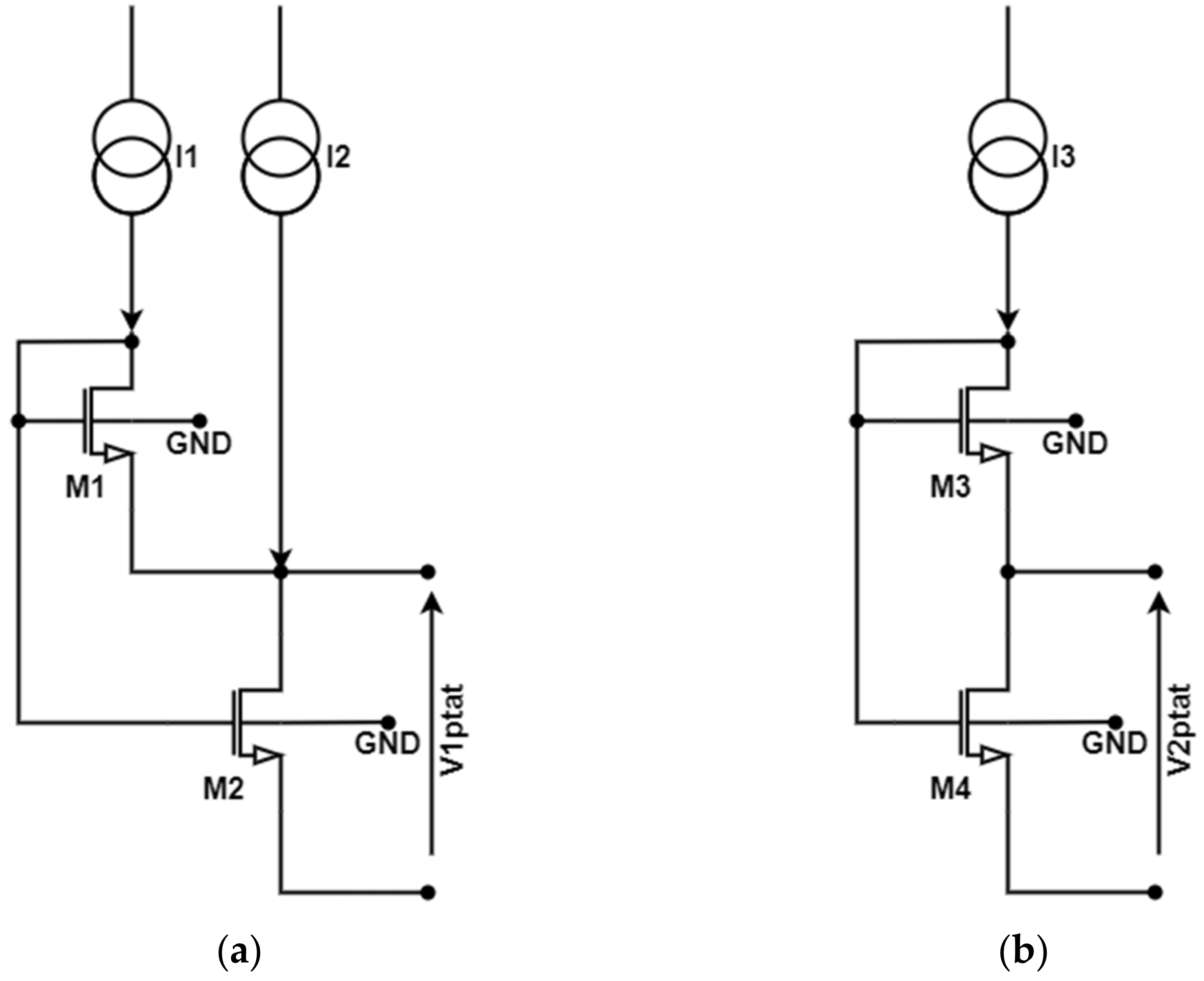
Various practical realizations of PTAT sensors, in which the resulting output voltage is proportional to the absolute temperature, are provided in the literature [8,9,10,11,12,13]. The original designs are based on bipolar transistors or p-n diodes of different sizes. One can also find solutions based only on the MOS transistors, which are achieved in CMOS technologies [23,24,25,26,27]. In such sensors, the PTAT voltage source consists of two n-type metal–oxide–semiconductor (NMOS) transistors, as presented in Figure 1. When two separate current sources are used, as in Figure 1a, both transistors operate in the weak inversion region and, then, one can derive the following equation [8]:
where Vptat—output voltage; T—absolute temperature; k—the Boltzmann constant; q—elementary charge; W1, W2, L1, and L2—the respective widths and lengths of transistor M1 and M2 channels; and I1 and I2—source currents.

Figure 1.
Electrical schematics of a PTAT sensor: (a) operating in the weak inversion region [8]; (b) operating in the strong inversion region [9].
The output sensor voltage Vptat in this equation is linearly dependent on the absolute temperature. The linear coefficient value depends on the MOS transistor aspect ratio W/L and the value of the source currents I1 and I2. The main advantages of this kind of sensor are its low-power dissipation and the small layout area.
When only one current source is used, as in Figure 1b, the output voltage is equal to [9,28]:
where T—absolute temperature, TR—reference temperature (300 K), IR—drain current at the reference temperature, S—W/L ratio (lower transistor M4), nR—subthreshold slope factor at the reference temperature, µR—effective electron mobility at the reference temperature, COX—NMOS gate oxide capacitance.
3. Sensor Design
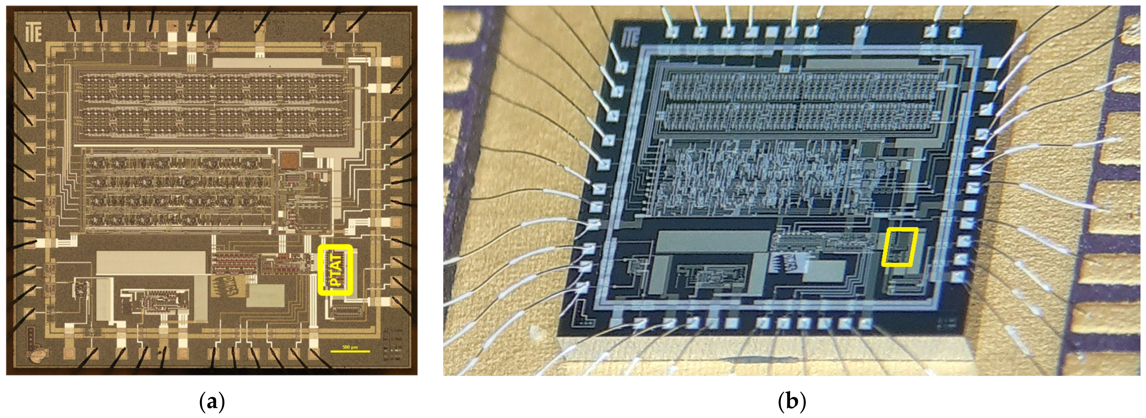
The PTAT sensor, as mentioned before, was designed as a part of a larger test ASIC manufactured using the 5 V 3 µm CMOS technology available in Poland. The ASIC was mounted in a ceramic DIL-40 package (Lukasiewicz Institute, Warsaw, Poland). The ASIC layout and its microscopic photograph taken with its package lid open are shown in Figure 2. The exact dimensions of the silicon die were 2080 μm × 2160 μm. The location of PTAT sensor, which is the main interest in this paper, is indicated in the figure with yellow boxes.
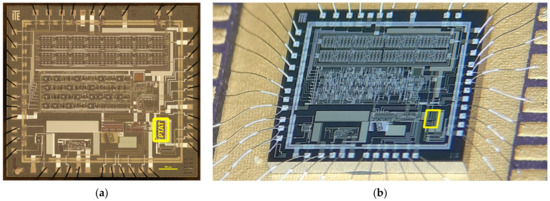
Figure 2.
ASIC design: (a) circuit layout; (b) microscopic photo of packaged chip.
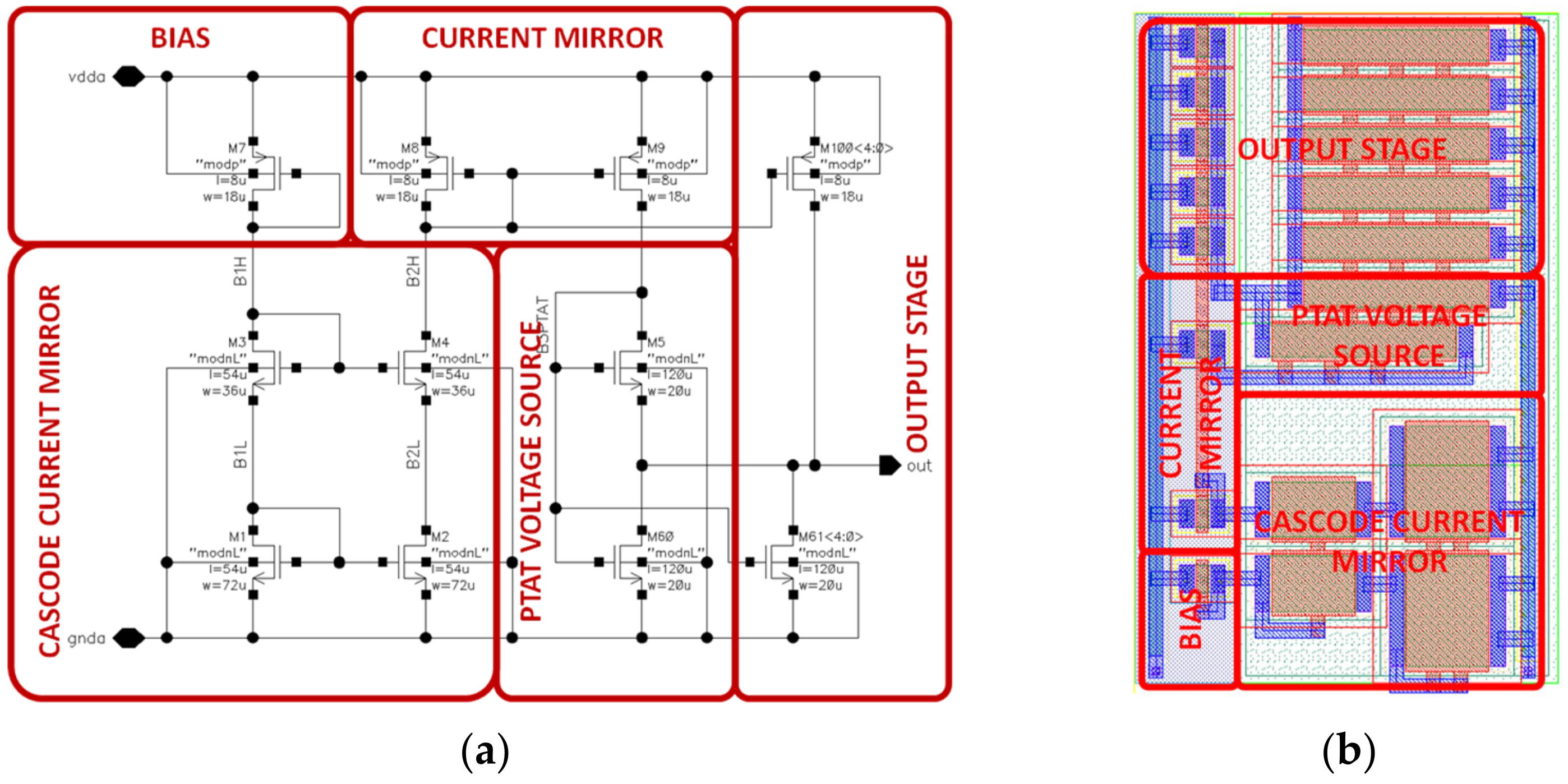
The electrical schematic of the PTAT sensor and its layout are presented in Figure 3. As it can be seen, it contains several blocks, including the diode-connected MOS providing sensor bias, two current mirrors, the actual PTAT voltage source, and the output stage. Taking into account the unavailability of bipolar transistors in the particular technology considered in this paper, only MOS transistors were used in the design. The entire PTAT sensor layout had the dimensions of 440 μm × 275 μm and it occupied an area of 0.121 mm2, which is just 2.7% of the entire chip area.
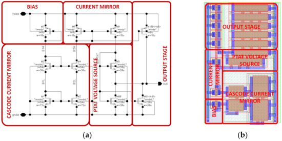
Figure 3.
PTAT sensor design: (a) electrical schematic; (b) sensor layout.
The ASIC that contains the PTAT sensor is composed of several functional blocks having separate power supply and ground lines. Thus, the influence of other components on the PTAT sensor can be eliminated simply by not powering them. The PTAT sensor is placed close to one of the ASIC corners (Figure 2). Such a location additionally minimizes the influence of other heat sources in the ASIC when they are powered. On the other hand, the PTAT is placed close to the electro-thermal filter (ETF). Both the resistor heater and the thermopile in this device can be used as heat sources with controlled power levels. Thus, it is possible to record the reaction of the PTAT sensor due to the dissipation of known amounts of energy in the proximity of the PTAT sensor.
Moreover, the electro-static discharge (ESD) protection devices of the ETF heater and thermopile are placed next to the PTAT sensor. Owing to such a location, the ESD devices also can be used as heat sources for the PTAT when the ETF is driven with currents that are high enough to switch on the ESD devices. This mode of operation was tested several times and the paper includes results obtained with activated ESD devices. Such an activation is safe and fully reversible when the ETF components are current-driven. The current–voltage characteristics of the ESD devices are highly non-linear and the current control mode enables a much better control of power dissipation in these devices.
Assuming a power dissipation limit of less than 0.5 mW for the nominal supply voltage of 5 V, it yields a maximal current equal to 100 µA. This assumption resulted in the PTAT electrical schematic presented in Figure 3. The main part of the sensor consists of two NMOS transistors M5 and M60, where the latter transistor has the aspect ratio W/L equal to 20 μm/120 μm. The M7 transistor biases the M1 and M3 transistors with the current of 8.5 μA. Together with the M2 and M4 transistors, they form a cascode current mirror replicating the current flowing through its left part. Owing to the cascode’s high resistance, independent of the circuit temperature or technology, the cascode ensures a high output sensor linearity [29,30]. The second current mirror formed by the M8 and M9 transistors was used in this paper for reversing the current that flowed through the M5 and M60 transistors. Because of the use of micrometer-sized technology, various channel length modulation and drain-induced barrier-lowering effects, discussed in [31], could be neglected in this paper. The output stage rendered the entire sensor less sensitive to the external readout circuitry.
4. Simulation and Measurement
Before the ASIC manufacturing, the PTAT sensor operation was simulated in the Cadence environment [32]. The results of corner analysis, presented in Figure 4, show that, in spite of the process parameter spread, the output voltage linearity remains virtually the same in a wide range of temperature values, from −25 °C to +125 °C. Namely, the PTAT sensor output voltage level shift between the maximal corner and the minimal corner is about 260 mV, but the sensor output voltage changes due to the temperature variation within the considered range are 217 mV and 221 mV for the respective corners.
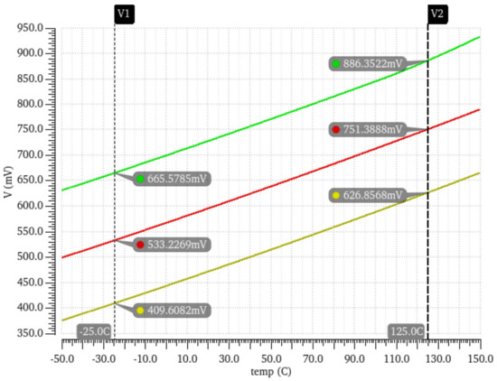
Figure 4.
The corner simulation graph (nominal corner—red line, maximal corner—green line, and minimal corner—yellow line).
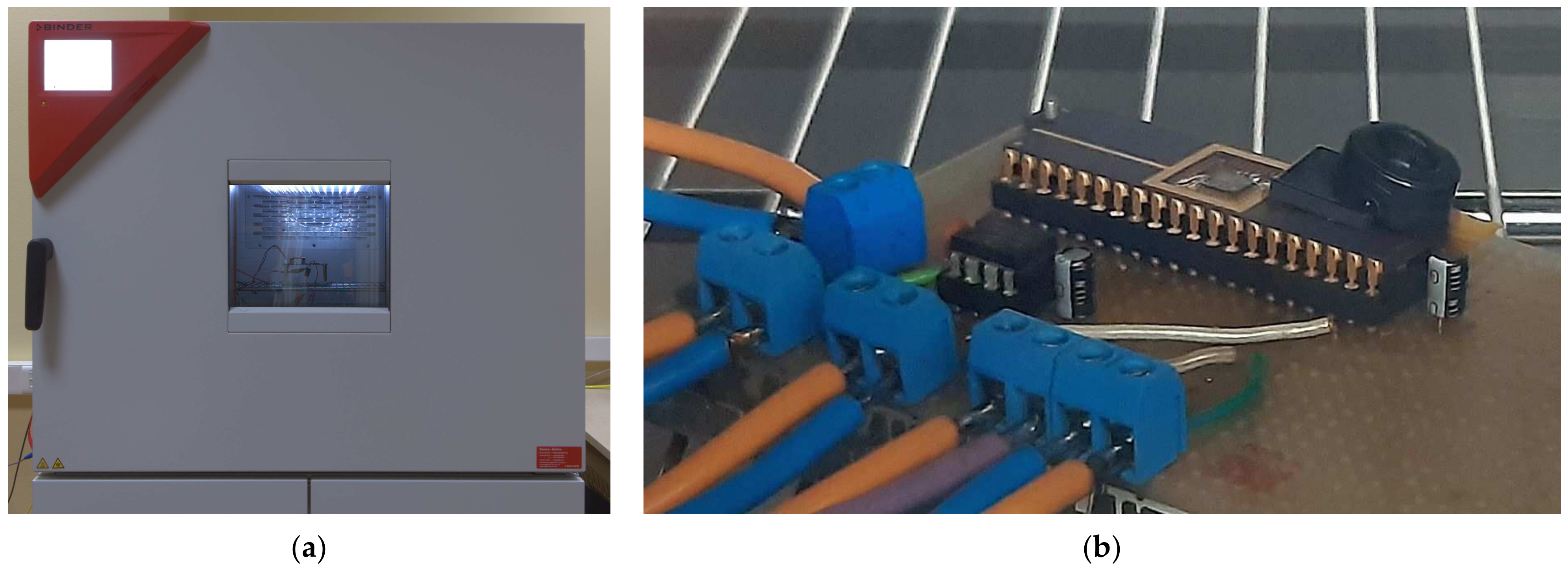
The actual dependence of the PTAT sensor voltage on the temperature was measured in the climate chamber Binder MKF 115 presented in Figure 5a. This chamber allows temperature measurements from −40 °C, to +180 °C with the pre-set air humidity value between 10% and 98% [33]. The measurements were taken for several ASIC samples in the temperature range from −40 °C to +150 °C.
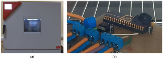
Figure 5.
PTAT sensor temperature calibration: (a) general view of the climate chamber; (b) the ASIC in the chamber with the lid removed.
First, the ASICs were placed in the chamber, cooled to −40 °C, and then maintained at this temperature for 20 min. Next, the temperature was ramped linearly up to +150 °C taking measurements during the heating process. Owing to the slow rate of the temperature increase of less than 1 °C/min, it was possible to ensure a low temperature difference between the environment and the measured ASICs. Moreover, in order to further minimize this difference, the measurements were taken with the package lid removed and the die exposed directly to the environment, as shown in Figure 5b.
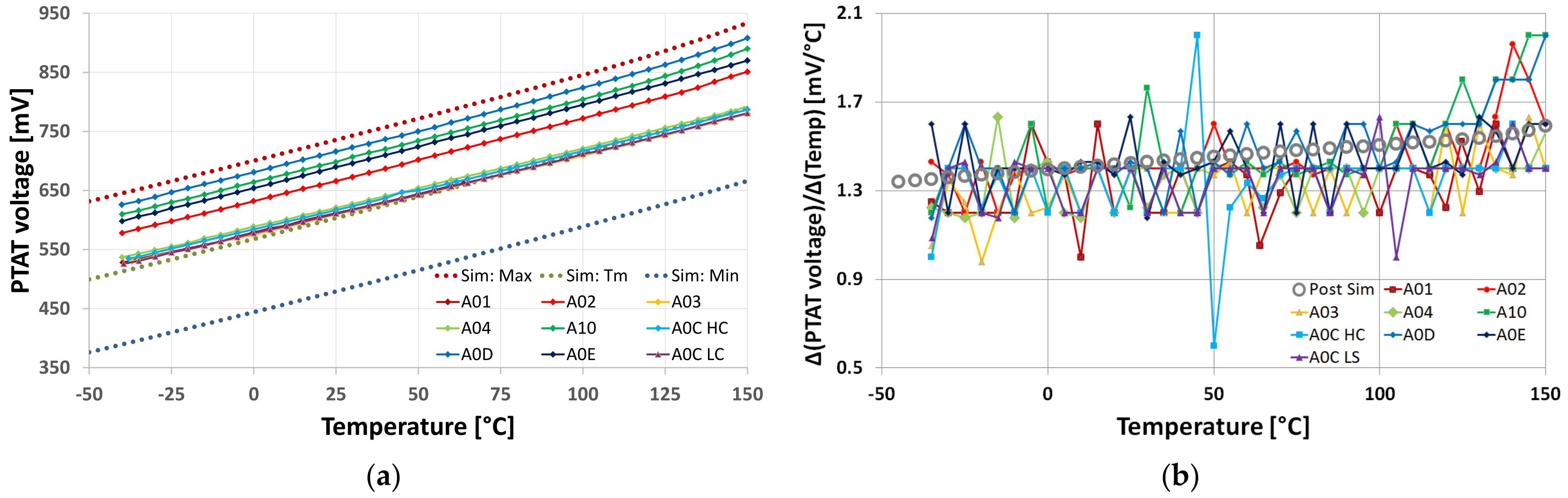
Each measurement session lasted nearly 6 h in order to acquire an output signal of high resolution. The actual measurements of the PTAT output voltage were taken with the resolution of 0.1 °C, but in this section, for the sake of picture clarity, the charts present the results at 5 °C intervals. Figure 6a comprises the measurement results for eight PTAT specimens named according to the pattern AXX (solid lines with markers). The letters and numbers denote particular ASIC specimens, each of them containing a single PTAT sensor. All these ASICs were supposed to be identical and behave in the same manner.
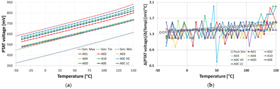
Figure 6.
The measured PTAT sensor characteristics compared with the results of the post-layout corner simulations: (a) the output voltage temperature dependence; (b) the derivative of the output voltage temperature dependence.
The measurement results were compared with the post-layout simulation results performed for the minimum, typical, and maximum corners (dotted lines). Post-layout simulations were carried out using parameters extracted based on the knowledge of IC layout and its geometry. The parameter extraction procedure provided information on parasitic resistances and capacitances identified in the IC geometry. The resulting netlist comprised all these parasitic devices and rendered possible more accurate analyses of circuit operation in both the direct current (DC) and alternating current (AC) domains.
As it can be observed in Figure 6a, the measured results are within the limits set by the post-layout simulation corners and primarily lie between the typical and maximum corners. The PTAT sensor output voltage linearity can be more precisely assessed by analyzing Figure 6b and comparing the derivatives of this voltage with respect to the temperature for all measured specimens (solid lines with markers) with the ones calculated based on the post-layout simulation (grey circles). The output voltage derivatives emphasize the non-linear effects, what makes the analysis more effective. As it can be seen, the sensor output voltage does not depend linearly on the temperature throughout the entire temperature measurement range, since the simulated sensitivity gradually increases, especially for temperature values exceeding 100 °C. The derivatives calculated based on the measurements, though very noisy due to the limited precision of meters, match quite well the simulated values.
5. Result Analysis and Discussion
Firstly, the linearity of the sensor was assessed by adding trendlines and calculating the determination coefficient R2 values for each curve in Figure 6a. The linear fitting results are also summarized in Table 1. As it can be seen, the determination coefficient values calculated for the measured and simulated values agree very well. Although the fitting results seem satisfactory, some non-linearity can be observed, especially at higher temperature values.

Table 1.
Linear fitting results of the PTAT output voltage temperature dependences presented in Figure 6a.
According to Equation (2), a linear thermal dependence of the PTAT sensor output voltage on the temperature should be expected, i.e., the derivative values in Figure 6b should be constant. On the other hand, both the post-layout simulation and the measurements show that these values increase with the temperature. Hence, this issue was investigated in more detail in the remainder of this paper.
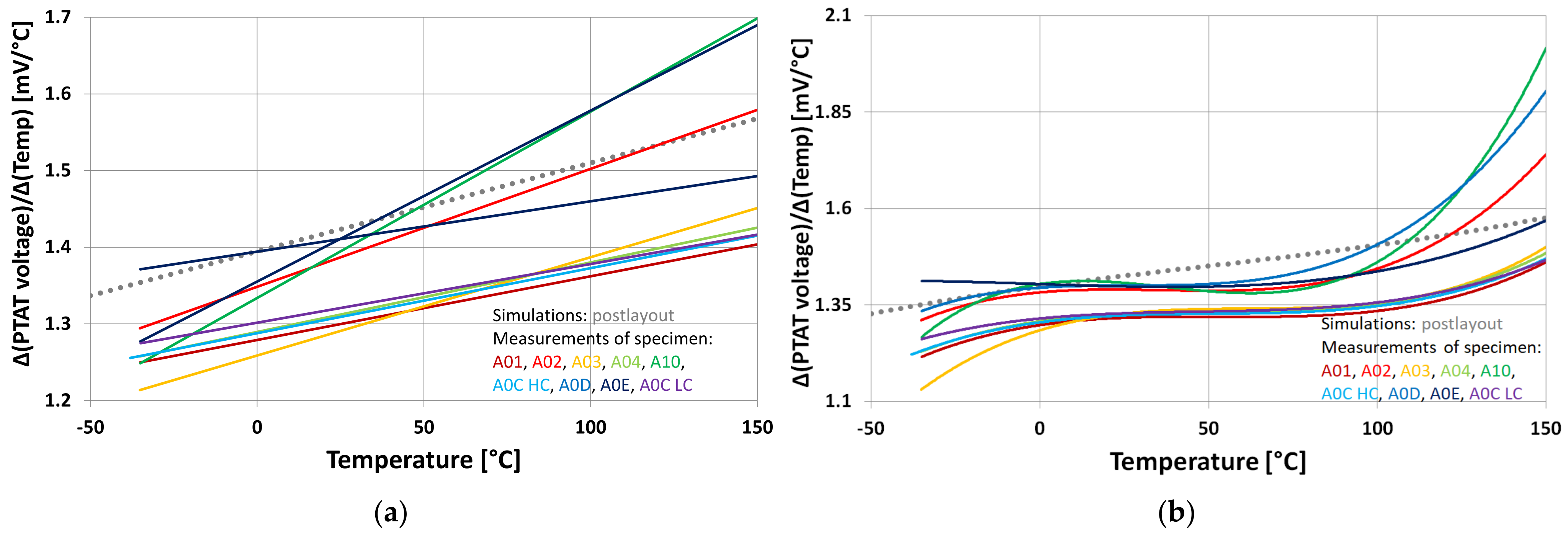
For this reason, first- and third-order polynomial fittings were carried out for the data concerned in Figure 6b. The latter fitting was expected to better represent the measured values. The results of this fitting are presented in Figure 7 and Table 2. The trendlines, as it can be seen, for any type of fitting can be divided into two distinct sets having different line slopes, flatter and steeper than the simulated trendline. Furthermore, the differences among the various ASIC specimens become even more pronounced at high temperature values. This might result from the fact that the tested chips belonged to different manufacturing batches.
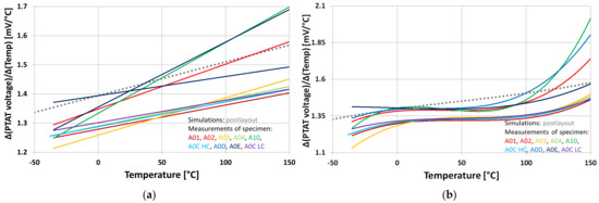
Figure 7.
Fitting results for the derivative of PTAT output voltage thermal dependence: (a) linear; (b) third-order polynomial.
Table 2.
Fitting results of the PTAT output voltage temperature dependence derivative in Figure 7.
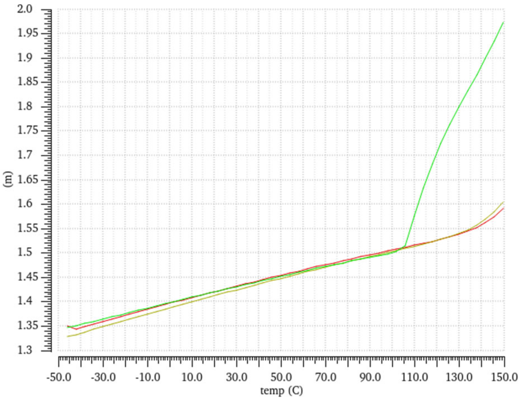
Non-linear effects are visible both in the results of the MAX corner simulation and the measurements. Additionally, this phenomenon was reproduced in the simulations, assuming that the PMOS transistors widths were greater than their nominal values (see the green line in Figure 8). Then, the drain current of transistor M9, visible in Figure 3, decreases at high temperature values and this device leaves the saturation region of its operation. On the other hand, the drain current of transistor M60 remains unchanged. This current difference is compensated by the current provided from the output stage of the PTAT sensor, which changes the output voltage. This occurs at temperature values exceeding 100 °C. Therefore, the non-linearities observed at high temperature values for some ASICs could be attributed to the technological process, rather than to the errors in the sensor design.

Figure 8.
The corner simulation graph with the effect of non-linearities at higher temperatures (Y-axis: value of the derivative of the sensor output voltage; X-axis: temperature in degrees Celsius) (nominal corner—red line, maximal corner—green line, and minimal corner—yellow line).
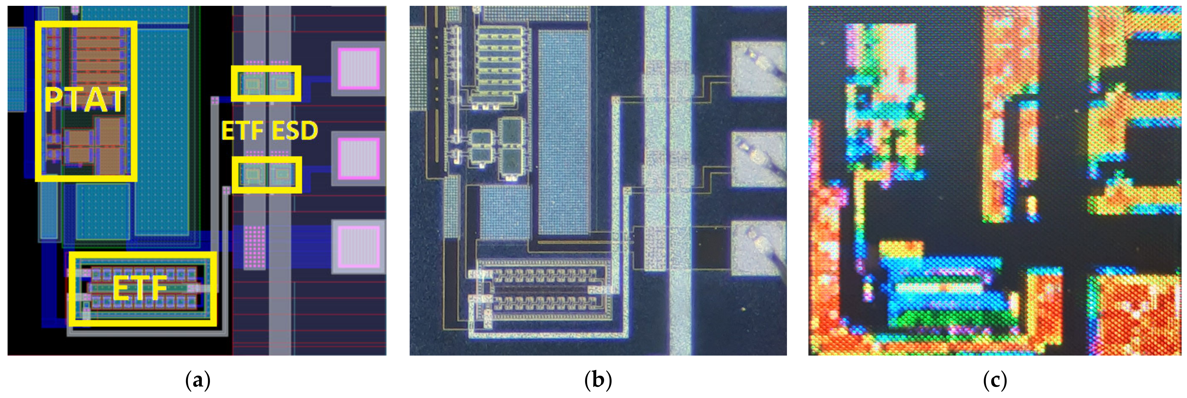
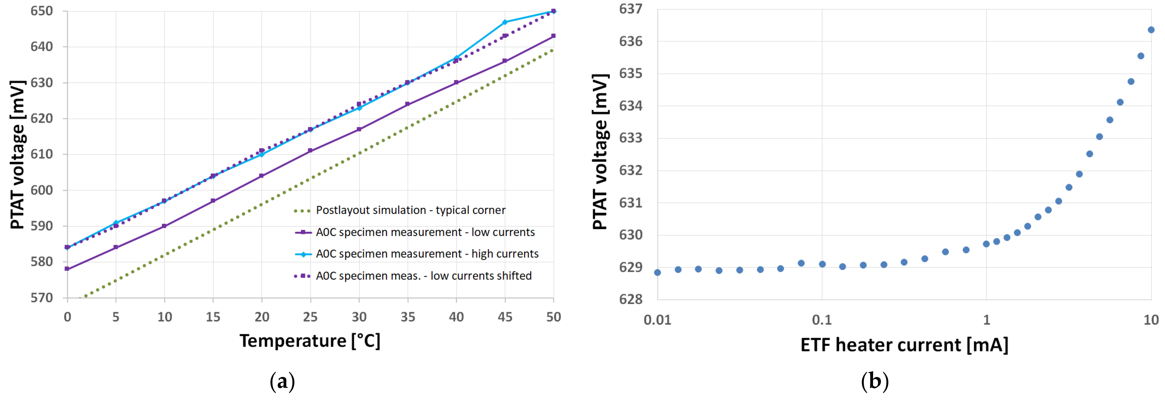
Additionally, the PTAT sensor behavior was analyzed using, instead of the climate chamber, the neighboring ETF and its ESD protection circuitry, highlighted by yellow boxes in Figure 9, which served as the heat sources. The ETF itself consists of a diffusion resistor heater and a temperature-sensing thermopile. For the sinusoidal excitation, the phase shift introduced by this device depends linearly on the temperature; thus, it can be used also as a temperature sensor [34]. The influence of the ETF on the PTAT sensor operation can be observed already in Figure 6, which presents two different measurements of the A0C specimen taken for low and high bias currents of the ETF heater and thermopile, denoted as LC and HC, respectively. The low current values were the same both for the heater and the thermopile and equal to 31.6 µA. The high current values were determined by the maximum voltage allowed at the temperature of 150 °C. These values amounted to 3.1 mA for the heater and 4.4 mA for the thermopile.

Figure 9.
The detailed view of the PTAT sensor, the ETF, and its ESD protection circuitry: (a) layout; (b) microscopic photo; (c) infrared image.
More detailed analyses of Figure 6a show that the low and high current thermal responses for the A0C specimen look nearly identical, but they are just shifted by about 5 °C from each other. This can be better observed in Figure 10a, which shows the measured temperature responses for the cases considered in this paper in the range of temperature from 0 °C to +50 °C. Additionally, the low current response shifted by 5 °C is also presented here. As it can be seen, after shifting, both PTAT sensor responses are almost identical.
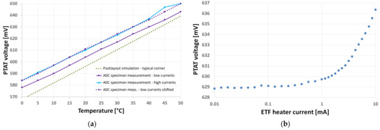
Figure 10.
PTAT output voltage for the A0C specimen: (a) temperature dependence for the low and high bias currents of the neighbouring ETF; (b) variation in the ETF thermopile voltage with the heater current.
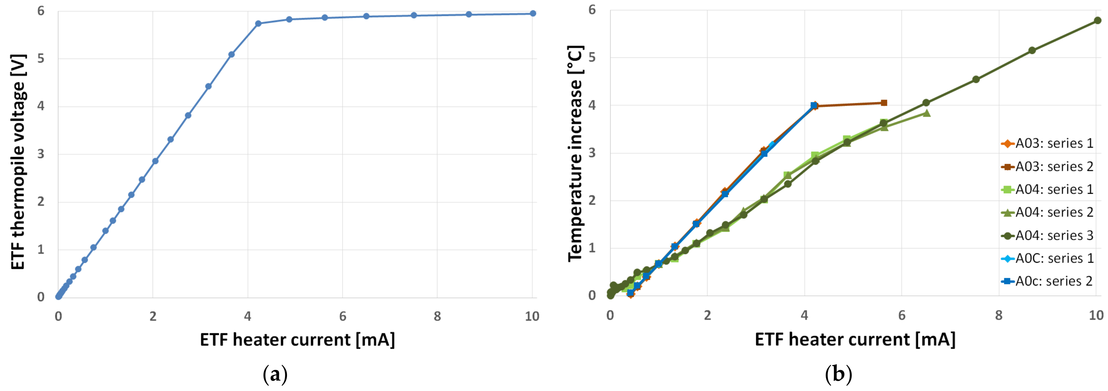
These analyses provided the incentive to conduct more thorough investigations of the PTAT output voltage dependence on the ETF heater current. Indeed, the measurements carried out for the A04 specimen, whose ASIC results are presented in Figure 10b, showed that the PTAT output voltage increased with the heater current and, for the value of 10 mA, the voltage change exceeded 7 mV.
Analyzing the operation of the ETF, as shown in Figure 11a, the output voltage generated by the thermopile increases with the heater current, but at the current value of slightly above 4 mA, the ETF voltage response saturates and finally sets at the value of about 5.8 V. This phenomenon can be explained by the activation of the ESD protection circuitry built in the heater input pad and consisting of two oppositely connected diodes sinking the excessive input current whenever an overvoltage event occurs.
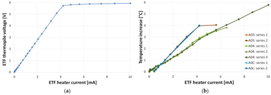
Figure 11.
Influence of the ETF heater current on: (a) the ETF thermopile voltage; (b) the calculated PTAT temperature measurement error.
The dependence of the PTAT output voltage on the ETF heater current was measured altogether for three different ASICs, A03, A04, and A0C, at least twice for each specimen. Then, using the linear fit equations presented in Table 2, the temperature measurement errors due to the observed PTAT sensor output voltage shift were calculated. The results of these calculations are presented in Figure 11b. Although the repeated measurement sessions in the case of each particular ASIC produced nearly identical results, there were clear differences between the different ASICs. Considering the temperature measurement error values, for the heater current of 10 mA, they amounted to 6 °C.
An additional check was performed also for whether the thermopile current influenced the PTAT output voltage. During these tests, both the ETF thermopile and the heating resistor were used for heating, or either of these devices. The obtained results were always referenced to the case when the ETF was not active. The heating resistor and thermopile current values during tests were equal to 3.1 mA and 4.4 mA, respectively; thus, they were identical to the earlier determined high bias current values for the A0C ASIC.
Then, considering that their resistances were equal to 1350 Ω and 950 Ω, the respective power values were 13.0 mW for the heater and 18.4 mW for the thermopile, yielding a dissipated power ratio of around 1.42. At the same time, the calculated temperature measurement error ratio was equal to 1.38; hence, the currents of both ETF devices have a comparable influence on the PTAT sensor measurement errors.
Similar experiments were also carried out with the A04 ASIC specimen. The results of all tests are summarized in Table 3. The PTAT sensor voltage shift and the resulting temperature measurement errors, as it can be seen, are comparable for both tested ASIC specimens, although the A0C one seems to be slightly more affected by the ETF current heating.
Table 3.
PTAT output voltage variation and temperature measurement errors due to the ETF current.
Therefore, the PTAT sensor investigated in this paper was compared with selected previous publications presenting similar sensors manufactured using CMOS technologies. The data presented in Table 4 show that, in spite of the apparently obsolete technology used for the design of the sensor, its layout area is fairly small and, what is even more important, its output characteristics are linear in a wide range of temperature values.
Table 4.
Various PTAT sensors’ comparison.
6. Conclusions
This paper presented a PTAT sensor designed and manufactured entirely using CMOS technology. The sensor operation was tested in the wide range of temperature values. The measurements carried out for several specimens of manufactured circuits confirmed the proper sensor operation. Its characteristics fell well within the limits defined by the post-layout corner simulations. Moreover, the output signal of the PTAT sensor turned out to be nearly linear over a wide temperature range. Thus, this technology can be considered repeatable and suitable for the production of small batches of analogue ICs.
However, the measurements showed that the apparent spread of the PTAT output voltage may require initial calibration in the case when the PTAT sensors are supposed to directly provide information on the temperature. Nevertheless, considering the measured temperature dependence of the PTAT output voltage, such a calibration should be rather a straightforward procedure. However, it should be noted that there are differences between various specimens of the measured PTAT, which seem to group them into a few batches. Thus, taking into account the process parameter spread, all PTAT sensors must be individually calibrated, especially for temperatures values exceeding 100 °C, when non-linear effects are observed.
The PTAT voltage source in the investigated sensor was generated by the M5 transistor operating in the saturation region and the M60 transistor operating in the linear region. The main advantage of this solution is a more stable operation and better immunity to the process parameter spread than in the solution when both transistors operate in the subthreshold region. The transistors in the output stage could be rescaled, influencing in this way the output voltage offset.
Furthermore, the experiments demonstrated that, in integrated circuits, which combine several analogue subcircuits, special precautions have to be undertaken, so that the components do not interfere with each other. In particular, it was shown that the PTAT sensor output response can be affected by the currents used for the powering of the ETF heating resistor and biasing its sensing thermopile. Future work should be focused on the redesign of the PTAT sensor in order to reduce its size and minimize the effect of non-linear behavior in higher temperatures, which was identified in this work.
Author Contributions
Conceptualization, M.S. and M.J. (Mariusz Jankowski); Methodology, M.S. and M.J. (Mariusz Jankowski); Validation, M.S., M.J. (Mariusz Jankowski) and M.J. (Marcin Janicki); Formal analysis, M.S. and M.J. (Mariusz Jankowski); Investigation, M.J. (Mariusz Jankowski); Writing—original draft, M.S. and M.J. (Mariusz Jankowski); Writing—review & editing, M.J. (Marcin Janicki); Visualization, M.J. (Mariusz Jankowski). All authors have read and agreed to the published version of the manuscript.
Funding
This research received no external funding.
Data Availability Statement
Data can be found within the article.
Acknowledgments
The authors would like to extend their gratitude to partners from the Institute of Microelectronics and Photonics of the Łukasiewicz Research Network (formerly the Institute of Electron Technology) in Warsaw, Poland, where the investigated ASIC was manufactured. The authors would like also to thank colleagues from their university for helping in solving various technical problems during the development of the investigated circuit.
Conflicts of Interest
The authors declare no conflicts of interest.
References
- AnandTech–Apple Announces M2 SoC: Apple Silicon for Macs Updated for 2022. Available online: https://www.anandtech.com/show/17431/apple-announces-m2-soc-apple-silicon-updated-for-2022 (accessed on 7 August 2023).
- Tyagi, S. Moore’s Law: A CMOS Scaling Perspective. In Proceedings of the 2007 14th International Symposium on the Physical and Failure Analysis of Integrated Circuits, Bangalore, India, 11 July 2007; pp. 10–15. [Google Scholar] [CrossRef]
- Moore, G.E. Cramming More Components onto Integrated Circuits. Proc. IEEE 1998, 86, 82–85. [Google Scholar] [CrossRef]
- Szekely, V. Thermal Monitoring of Microelectronic Structures. Microelectron. J. 1994, 25, 157–170. [Google Scholar] [CrossRef]
- Elamaran, D.; Suzuki, Y.; Satoh, H.; Banerjee, A.; Hiromoto, N.; Inokawa, H. Performance Comparison of SOI-Based Temperature Sensors for Room-Temperature Terahertz Antenna-Coupled Bolometers: MOSFET, PN Junction Diode and Resistor. Micromachines 2020, 11, 718. [Google Scholar] [CrossRef] [PubMed]
- Makinwa, K.A.A.; Witte, J.F. A temperature sensor based on a thermal oscillator. In Proceedings of the SENSORS, 2005 IEEE, Irvine, CA, USA, 30 October–3 November 2005; p. 4. [Google Scholar] [CrossRef]
- Golovins, E.; Sinha, S. Analytical Approach to Design of Proportional-to-the-Absolute-Temperature Current Sources and Temperature Sensors Based on Heterojunction Bipolar Transistors. IEEE Trans. Compon. Packag. Manuf. Technol. 2013, 3, 262–274. [Google Scholar] [CrossRef]
- Wojciak, W. Implementacja Czujnikow Temperatury w Technologii CMOS i ich Zastosowanie do Termicznego Monitorowania Struktur Polprzewodnikowych (in English: ‘Implementation of Temperature Sensors in CMOS Technology and Their Application to Thermal Monitoring of Semiconductor Structures’). Ph.D. Thesis, Lodz University of Technology, Lodz, Poland, 1998. [Google Scholar]
- Rossi, C.; Aguirre, P. Ultra-low Power CMOS Cells for Temperature Sensors. In Proceedings of the 18th Annual Symposium on Integrated Circuits and System Design, SBCCI’05, Florianopolis, Brazil, 4–7 September 2005. [Google Scholar]
- Rossi, C.; Galup-Montoro, C.; Schneider, M.C. PTAT Voltage Generator based on an MOS Voltage Divider. NSTI-Nanotech 2007, 3, 2007. [Google Scholar]
- Chaparro, S.; Carrillo, J.J.; Alarcon, H. A high-slope PTAT temperature sensor for frequency compensation of an RTC oscillator. In Proceedings of the 2016 IEEE 7th Latin American Symposium on Circuits & Systems (LASCAS), Florianopolis, Brazil, 28 February–2 March 2016; pp. 111–114. [Google Scholar] [CrossRef]
- Lee, T.-J.; Tu, K.-H. Wide Dynamic Range Temperature Sensor Using High Sensitivity PTAT Current Generator. In Proceedings of the 2022 19th International SoC Design Conference, Gangneung-si, Republic of Korea, 19–22 October 2022; pp. 17–18. [Google Scholar] [CrossRef]
- Tewari, S.; Singh, K. Intuitive design of PTAT and CTAT circuits for MOSFET based temperature sensor using Inversion Coefficient based approach. In Proceedings of the 2015 19th International Symposium on VLSI Design and Test, Ahmedabad, India, 26–29 June 2015; pp. 1–6. [Google Scholar] [CrossRef]
- Chouhan, S.; Halonen, K. A Low Power Temperature to Frequency Converter for the On-Chip Temperature Measurement. IEEE Sens. J. 2015, 15, 4234–4240. [Google Scholar] [CrossRef]
- Azam, A.; Bai, Z.; Walling, J.S. An Ultra-Low Power CMOS Integrated Pulse-Width Modulated Temperature Sensor. IEEE Sens. J. 2021, 21, 1294–1304. [Google Scholar] [CrossRef]
- Yadav, A.; Bulusu, A.; Dasgupta, S.; Singh, S. Design and Fabrication of Rad-hard Low Power CMOS Temperature Sensor for Space Applications at 180 nm. In Proceedings of the 2021 International Conference on Microelectronics (ICM), New Cairo City, Egypt, 19–22 December 2021; pp. 166–169. [Google Scholar] [CrossRef]
- Szermer, M.; Janicki, M.; Kulesza, Z.; Napieralski, A. Practical realization of PTAT sensor for ASIC overheat protection. In Proceedings of the 2009 15th International Workshop on Thermal Investigations of ICs and Systems, Leuven, Belgium, 7–9 October 2009; pp. 80–83. [Google Scholar]
- Ali, A.; Kiran, S.; Jain, A.; Abbas, Z. A 47nW, 0.7–3.6V wide Supply Range, Resistor Based Temperature Sensor for IoT Applications. In Proceedings of the 2019 IFIP/IEEE 27th International Conference on Very Large Scale Integration (VLSI-SoC), Cuzco, Peru, 6–9 October 2019; pp. 293–298. [Google Scholar] [CrossRef]
- Law, M.K.; Bermak, A.; Luong, H.C. A Sub-uW Embedded CMOS Temperature Sensor for RFID Food Monitoring Application. IEEE J. Solid-State Circuits 2010, 45, 1246–1255. [Google Scholar] [CrossRef]
- Golda, A.; Kos, A. Parameters Identification of Embedded PTAT Temperature Sensors for CMOS Circuits. In Proceedings of the 2007 14th International Conference on Mixed Design of Integrated Circuits and Systems, Ciechocinek, Poland, 21–23 June 2007; pp. 392–395. [Google Scholar] [CrossRef]
- Łukasiewicz–Instytut Mikroelektroniki i Fotoniki, Warszawa, Poland. Available online: https://imif.lukasiewicz.gov.pl (accessed on 7 August 2023).
- Romiński, A.; Makowski, D.; Napieralski, A. Cyfrowy synchroniczny układ ASIC, jako detektor promieniowania neutronowego. Pomiary Autom. Kontrola R 2010, 56, 652–655. [Google Scholar]
- Tsai, J.T.-S.; Chiueh, H. High linear voltage references for on-chip CMOS smart temperature sensor from −60 °C to 140 °C. In Proceedings of the 2008 IEEE International Symposium on Circuits and Systems (ISCAS), Seattle, WA, USA, 18–21 May 2008; pp. 2689–2692. [Google Scholar] [CrossRef]
- Hung, C.-C.; Chu, H.-C. A Current-Mode Dual-Slope CMOS Temperature Sensor. IEEE Sens. J. 2016, 16, 1898–1907. [Google Scholar] [CrossRef]
- Zhai, S.; Li, W.; Liu, J.; Zhang, T. A Low Supply Sensitivity CMOS Temperature Sensor Using Dynamic-Distributing-Bias Circuit. In Proceedings of the 2022 IEEE International Conference on Integrated Circuits, Technologies and Applications (ICTA), Xi’an, China, 28–30 October 2022; pp. 180–181. [Google Scholar] [CrossRef]
- Wu, T.; Wang, X.; Bai, H.; Lin, Q. Room-temperature CMOS 4.2THz Thermal Detector Comprising a Metamaterial Absorber and a PTAT Sensor. In Proceedings of the 2022 IEEE 10th Joint International Information Technology and Artificial Intelligence Conference (ITAIC), Chongqing, China, 17–19 June 2022; pp. 1925–1929. [Google Scholar] [CrossRef]
- Serra-Graells, F.; Huertas, J.L. Sub-1-V CMOS proportional-to-absolute temperature references. IEEE J. Solid-State Circuits 2003, 38, 84–88. [Google Scholar] [CrossRef]
- Galup-Montoro, C.; Schneider, M.C.; Cunha, A.I.A.; de Sousa, F.R.; Klimach, H.; Siebel, O.F. The Advanced Compact MOSFET (ACM) Model for Circuit Analysis and Design. In Proceedings of the 2007 IEEE Custom Integrated Circuits Conference, San Jose, CA, USA, 16–19 September 2007; pp. 519–526. [Google Scholar] [CrossRef]
- Razavi, B. Design of Analog CMOS Integrated Circuits; McGraw-Hill: Singapore, 2001. [Google Scholar]
- Jacob Baker, R. CMOS Circuit Design, Layout, and Simulation, 3rd ed.; Wiley-IEEE Press: Hoboken, NJ, USA, 2010. [Google Scholar] [CrossRef]
- De Vita, G.; Iannaccone, G. A sub-1-V, 10 ppm/°C, nanopower voltage reference generator. IEEE J. Solid-State Circuits 2007, 42, 1536–1542. [Google Scholar] [CrossRef]
- Cadence: EDA Tools and IP for System Design Enablement. Available online: https://www.cadence.com (accessed on 7 August 2023).
- Binder GmbH-Drying and Heating Chambers, Tuttlingen, Germany. Available online: https://www.binder-world.com (accessed on 7 August 2023).
- Xia, S.; Makinwa, K. Design of an optimized electrothermal filter for a temperature-to-frequency converter. In Proceedings of the SENSORS, 2007 IEEE, Atlanta, GA, USA, 28–31 October 2007; pp. 1255–1258. [Google Scholar]
- Leung, K.N.; Mok, P.K.T. A sub-1 V 15 ppm/q C CMOS Bandgap Voltage Reference without Requiring Low Threshold Voltage Device. IEEE J. Solid State Circuits 2002, 37, 526–530. [Google Scholar] [CrossRef]

Disclaimer/Publisher’s Note: The statements, opinions and data contained in all publications are solely those of the individual author(s) and contributor(s) and not of MDPI and/or the editor(s). MDPI and/or the editor(s) disclaim responsibility for any injury to people or property resulting from any ideas, methods, instructions or products referred to in the content. |
© 2024 by the authors. Licensee MDPI, Basel, Switzerland. This article is an open access article distributed under the terms and conditions of the Creative Commons Attribution (CC BY) license (https://creativecommons.org/licenses/by/4.0/).