Abstract
This paper proposes a harmonic-suppressed Wilkinson power divider (HS WPD) utilizing parallel resonant shunt stubs (PRSSs). PRSSs are integrated into the conventional WPD by adding functionalities such as bandpass filtering, harmonic suppression, and physical port separation. The resonance conditions and design equations of the PRSS are theoretically derived and verified through circuit simulations. Using the PRSS, we designed an HS WPD operating at 1 GHz. The fabricated HS WPD demonstrated an insertion loss of 3.2 dB at the fundamental frequency, with a wide 3 dB bandwidth of 129%. The harmonic suppression levels at the 2nd and 3rd harmonic frequencies are measured to be 21.0 dB and 25.8 dB, respectively. The measured input return loss at the fundamental frequency was 27.9 dB, whereas the output return loss was 24.6 dB. Additionally, the HS WPD demonstrates isolation levels at the fundamental, 2nd, and 3rd harmonic frequencies, with levels of 29.2 dB, 17.8 dB, and 47.1 dB, respectively. It also exhibited broadband isolation (>8.7 dB) across the frequency range of 100 kHz to 3.35 GHz. The PRSS design allows for the physical separation of the ports without requiring additional circuitry. Compared to previously reported PDs, the proposed design offers multiple functions in a compact size, making it highly suitable for various microwave systems.
1. Introduction
Power dividers (PDs) are essential components of microwave systems that distribute signals among multiple paths. The Wilkinson power divider (WPD), introduced in 1960, achieves equal power distribution, impedance matching, and isolation by using two quarter-wavelength transmission lines and a resistor [1]. Circuit simplicity and excellent performance have been widely adopted in microwave applications, including power amplifiers, frequency multipliers, and phased–array antennas [2,3,4]. To further enhance the performance of WPDs, extensive research has been conducted to incorporate additional functions [5,6,7].
There has been research on integrating resonator or bandpass filters (BPFs) into PDs to establish compact RF front-end systems using two or more coupled lines [6,7,8,9,10,11,12,13,14,15]. For instance, in [8], a filtering power divider (FPD) was introduced, using three–line coupled structures, achieving effective frequency selectivity with a 3 dB insertion loss bandwidth of 82.6%. In [9], a multiway FPD using n–coupled multimode resonators and resistors was proposed, demonstrating excellent frequency selectivity with a 1-dB insertion loss bandwidth of 49%. However, it is challenging to accurately control the coupling factors of the coupled lines in FPDs [12]. An FPD with an enhanced power dividing ratio of 8.1:1 and a 10-dB return loss fractional bandwidth of 97.5% was proposed using a triple–mode resonator [13]. A compact triple–band FPD was introduced using short–circuited step–impedance resonators was introduced in [14]. Unfortunately, these FPDs often suffer from complex circuit layouts with numerous design variables, which pose challenges in terms of design, manufacturing, and optimization.
Harmonic suppression filters have also been integrated into PDs to reject harmonic components of the input signal [16,17,18,19,20,21,22,23,24,25,26]. This is because the harmonic signals generated by nonlinear circuits, such as power amplifiers and mixers, adversely affect the overall system performance. The WPDs also demonstrate a good transmission performance at harmonic frequencies due to the periodicity property of the transmission lines. Various techniques have been proposed for harmonic–suppressed PDs (HS PDs), such as a defected ground structure (DGS) [18,19], DGS with split–ring resonators [20], microstrip electromagnetic bandgaps [21], and open stubs embedded in the central transmission line [22]. However, these techniques often require the addition of metallic patterns to the ground or bottom plane, resulting in increased fabrication costs. A novel design method employing an artificial neural network to optimize the frequency response of a Wilkinson power divider incorporating T–shaped resonators was proposed in [23]. It enables a 45% reduction in size compared to conventional WPD (CWPD) and suppression of signals up to the 5th harmonic. In [24], a compact PD utilizing low–pass filters was reported, achieving harmonic suppression from the 2nd to 6th order with a suppression level exceeding 20 dB. In [26], a power divider utilizing a highly tailored low–pass filter (LPF) was used for LTE and GSM applications. It shows excellent harmonic suppression capabilities from the 2nd to 7th harmonics, with a suppression level of over 20 dB, albeit without exhibiting BPF characteristics.
The WPDs suffer from poor physical separation between output ports because of the isolation resistance between the two output ports [27]. As a result, the electrical isolation can also be compromised due to the coupling between two quarter–wave long transmission lines. Additionally, the need for additional transmission lines to connect the WPDs with other circuits leads to an increased insertion loss and circuit size. Various modifications have been proposed to separate the output ports, such as incorporating complex isolation networks within quarter–wave transmission lines [27,28,29,30,31,32] or introducing additional transmission lines between the output ports [33,34]. However, these methods are bulky and do not facilitate the implementation of a BPF response.
Several PDs have been proposed to address these problems [11,12,16]. In [11], a modified parallel-coupled structure incorporating stub-loaded resonators and stepped-impedance coupled lines was utilized for a bandpass filter response and harmonic suppression, achieving a compact size with a wide passband of 57.1% for 3 dB insertion loss and a stopband of 101% for 40 dB attenuation. In [12], a single open-type dual-mode resonator was employed to design a power divider with sharp frequency selectivity, wide upper stopband, and excellent in-band isolation performance. Ref. [16] proposed a compact power divider with enhanced 2nd harmonic suppression, based on a quasi-elliptic BPF using quarter-wavelength and half-wavelength resonators. However, these PDs generally exhibit a narrow 3 dB bandwidth performance and require a complex circuit layout with numerous design variables. Moreover, some of these designs may involve additional fabrication processes, leading to increased cost.
In this paper, we propose the use of parallel resonant shunt stubs (PRSSs) to achieve a bandpass filtering characteristics and harmonic suppression [35]. The PRSS consists of only two stubs, allowing for easy performance adjustment by controlling several parameters. Additionally, we introduce a harmonic suppressed WPD (HS WPD) that incorporates the PRSS. The proposed HS WPD operates as a CWPD at the center frequency, while providing additional functions such as dc suppression, harmonic suppression, and physical separation of output ports, distinguishing it from other previously presented WPDs. The theoretical analysis and simulated performance of the PRSS, based on the derived equations, are presented in Section 2. Section 3 focuses on the design of HS WPDs utilizing the PRSS. In Section 4, we present the fabrication and measurement results of the HS WPDs, including a performance comparison with previously reported PDs.
2. Analysis of Parallel Resonant Shunt Stub
The proposed PRSS configuration consists of an open stub and shorted stub connected in parallel, as shown in Figure 1. These stubs were designed to resonate at the center frequency (). The open stub exhibits capacitive impedance, whereas the shorted stub exhibits inductive impedance when their electrical lengths ( and ) are less than 90°, as represented by (1) and (2). The input impedances of the open stub (), the shorted stub (), and PRSS () are given by (1)–(3), respectively.
where and denote the characteristic impedance and electrical length of the open stub, respectively, and and represent those of the shorted stub. The PRSS resonates at a frequency where the sum of the reactances of the open and shorted stubs becomes zero, or equivalently, when approaches infinity, as indicated by (3). The resonance condition is expressed as (4).
where denotes the ratio of the characteristic impedance of the open stub to that of the shorted stub.
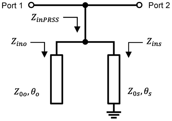
Figure 1.
Circuit schematic of parallel resonant shunt stub.
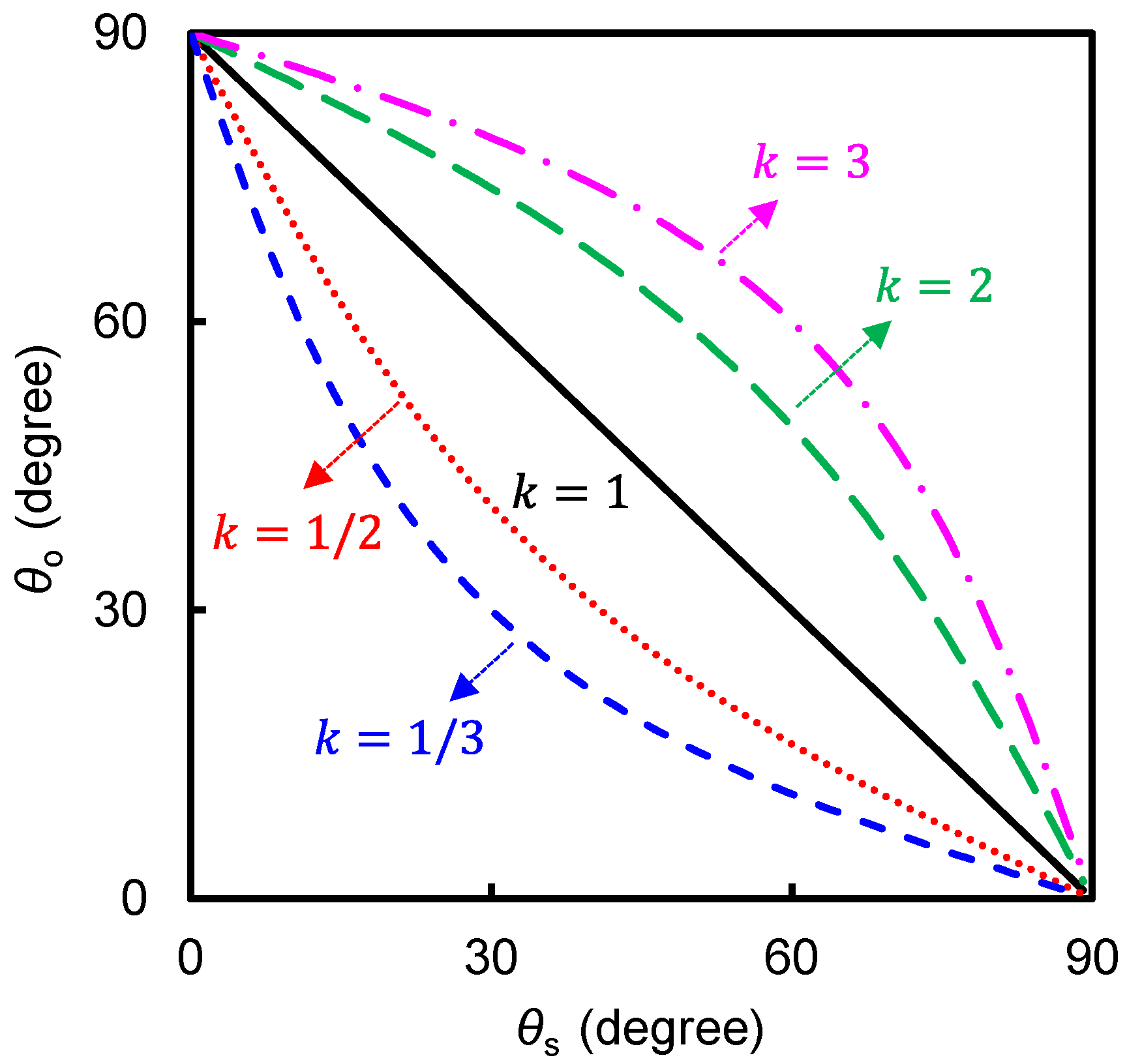
There are infinitely many combinations of , , and that satisfy Equation (4). Figure 2 illustrates the relationship between and , satisfying the resonance condition specified by Equation (4), at various values of : 1/3, 1/2, 1, 2, and 3. In this figure, and are constrained to values between 0 and 90° for simplicity. When = 1, indicating , the PRSS resonates if . As decreased from 1, the total electrical length of the PRSS, , also decreased from 90°, resulting in a reduction in the circuit size. Conversely, for values of greater than 1, the total electrical length exceeded 90°. This paper focused is on the case of 1, where , to reduce the circuit size. For a given 1, it can be proven from (4) that the total electrical length, , has a minimum value when . This simplifies (4) to (5).
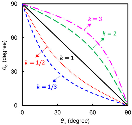
Figure 2.
Relationship between electrical lengths of open and shorted stubs, and , at various values of , meeting resonance condition.
Table 1 lists the calculated values of or given by Equation (5) for the corresponding values of : 1, 1/2, and 1/3. This demonstrates that smaller values of result in a reduction in the total electrical length.

Table 1.
Electrical length of open and shorted stub according to .
Based on Table 1 and the equations mentioned earlier, the PRSS was designed using ideal transmission lines, and its performance was predicted using the Advanced Design System (ADS) by Keysight, Inc. (Santa Rosa, CA, USA). Figure 3a illustrates the simulated S-parameters of the designed PRSS shown in Figure 1, where for different values of : 1, 1/2, and 1/3. The frequency was normalized to the center frequency, , which is also the resonant frequency of the PRSS.
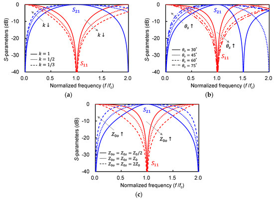
Figure 3.
Simulated characteristics of parallel resonant shunt stub. (a) S–parameters as a function of with and . (b) S–parameters as a function of with . (c) S–parameters as a function of characteristic impedance of PRSS with () and 45°.
The designed PRSS exhibited an open impedance at its resonant frequency and was connected in parallel with the signal path, resulting in a full transmission and perfect impedance matching at . As the frequency decreases from the resonant frequency, the impedance of the PRSS decreases because of the shorted stub. Conversely, the open stub reduces the input impedance of the PRSS as the frequency increases until it reaches the frequency at which the electrical length of the open stub becomes 90°.
In summary, the PRSS effectively operates as dc and 2nd harmonic suppression centered at , as illustrated in Figure 3a. It provides selective transmission of signals within the desired frequency range while attenuating frequencies outside this range.
Figure 3a also demonstrates that the bandwidth of the BPF expands as decreases, which is achieved by increasing while keeping fixed at . This occurs because the PRSS is connected in parallel with the signal path and a higher leads to an increased impedance when the frequency deviates from the resonant frequency. Moreover, as shown in Table 1, the electrical lengths of both stubs decrease at lower values of k, contributing to the widening of the bandwidth [36].
The PRSS effectively reflects the signal at dc through the shorted stub. When = 1, the open stub has an electrical length = 45° at , resulting in a short impedance at , providing a complete reflection, as illustrated in Figure 3a. Note that this null frequency can also be adjusted using , which is the ratio of the characteristic impedance.
Figure 3b shows the simulated S–parameters of the PRSS while varying from 30° to 75° in increments of 15°. In this simulation, was fixed at 1, which implies . The electrical length was adjusted according to to maintain the resonance condition at the center frequency. Consequently, the modified input impedances of the open and shorted stubs in (1) and (2) become
at the center frequency. Figure 3b demonstrates that the bandwidth of the PRSS expands as increases. This can be attributed to the fact that higher values of , as indicated by (6) and (7), result in large magnitudes of and at the center frequency, consequently leading to an increased at frequencies deviating from the center frequency. Furthermore, as increased, the frequency at which the open stub exhibited a short impedance also increased. For instance, at = 30°, there is a null in || at 1.5 , caused by the open stub with . This null frequency increases to 2 at = 45° (or = 45°), resulting in a broader bandwidth, as demonstrated in Figure 3b.
Figure 3c depicts the impact of the characteristic impedance of the open and shorted stubs on the transmission and reflection characteristics of the PRSS. In this simulation, was held constant at 1, implying . The electrical lengths and were both set to 45°. As the characteristic impedance of the PRSS increased from /2 to 2, the input impedance of the PRSS progressively increased, resulting in an increased bandwidth.
In summary, the proposed PRSS, which comprises only two stubs, offers a bandpass filtering capability, with the bandwidth adjustable based on the characteristic impedance and electrical lengths of the PRSS. For example, a broader bandwidth can be achieved by increasing the characteristic impedance and electrical length of a shorted stub. As a result, it can be easily designed with using equations involving a relatively small number of design variables. Furthermore, the PRSS boasts of a compact circuit size because it consists of only two stubs.
3. Design of Harmonic-Suppressed WPD
The proposed PRSS not only demonstrates bandpass filtering characteristics, as discussed earlier, but can also be applied to effectively suppress the harmonic components of the input signals. In this study, we utilized the PRSS to design multi-functional WPDs, specifically HS WPD. These designs offer the additional benefit of physically separating the output ports.
3.1. A-Type HS WPD Using PRSS
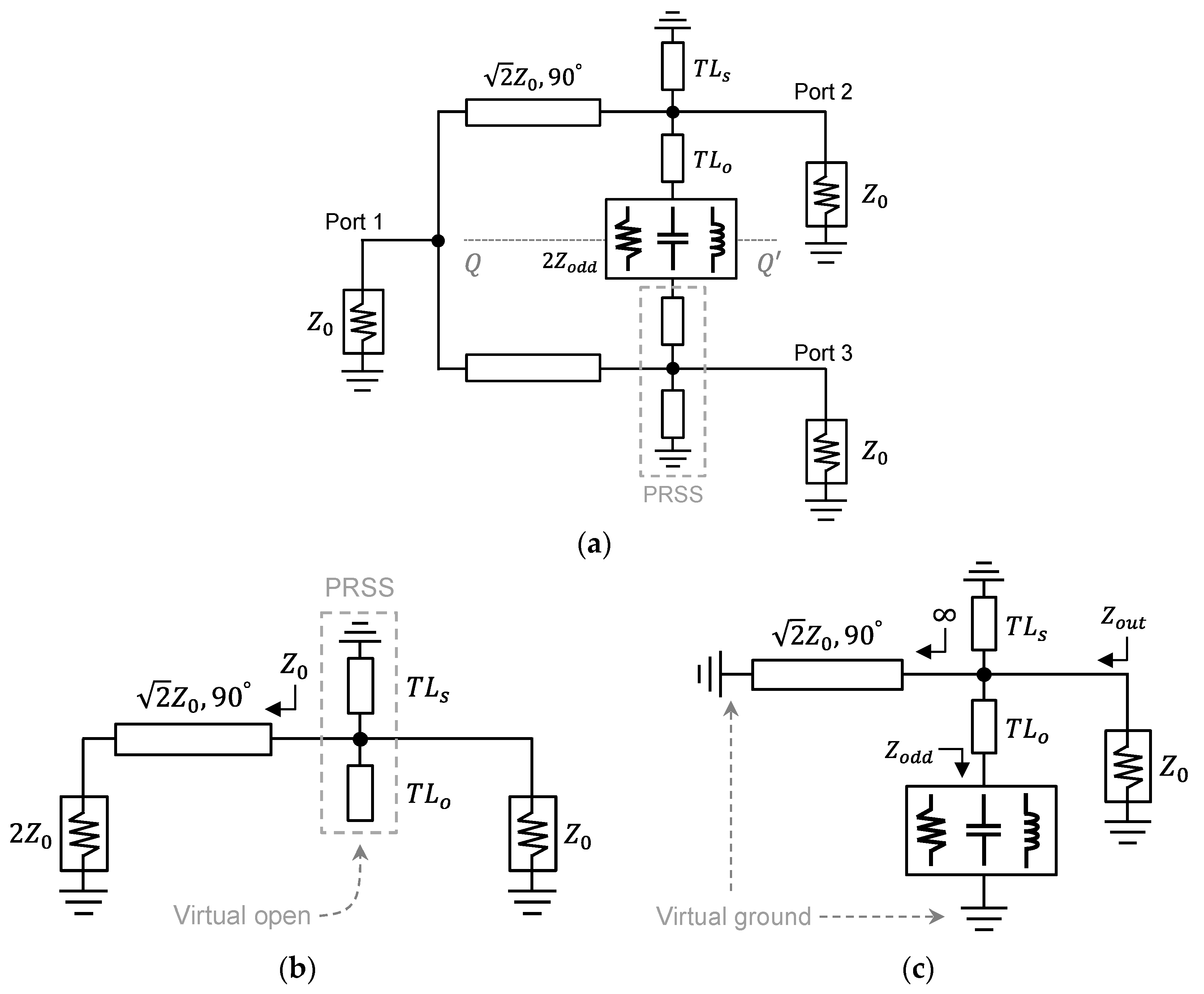
Figure 4a shows the circuit diagram of the A–type HS WPD, which integrates PRSSs ( and ) into the output ports of the CWPD. The isolation network was also modified to achieve a perfect isolation at the center frequency. Therefore, the proposed A–type HS WPD has the capability to operate as a bandpass filtering characteristic due to the inclusion of the PRSS circuits at the signal paths. Additionally, the combination of the PRSSs and an isolation network enables both physical and electrical isolation between the two output ports. Physical isolation indicates that the designed PD can offer compact and low-loss integration with other circuits [27].

Figure 4.
Design of A-type harmonic suppressed WPD using PRSS. (a) Circuit schematic. (b) Even-mode equivalent circuit. (c) Odd-mode equivalent circuit.
The operating principle can be analyzed using even– and odd–mode analyses. In the even-mode operation, a virtual open circuit is created along the symmetrical line QQ′, as shown in Figure 4a. Therefore, the even–mode equivalent circuit is obtained, as shown in Figure 4b, where the PRSS is formed at port 2 due to the open circuit at the isolation network. Except for the PRSS at port 2, Figure 4b is the same as the even–mode equivalent circuit of the CWPD. At the center frequency, the PRSS is open–circuited, and port 2 is impedance–matched to due to the quarter-wave long line of the CWPD.
In the odd–mode operation, a virtual ground is established along the QQ′ line, such that the equivalent circuit can be drawn, as shown in Figure 4c. In this case, the shorted quarter-wave long line of the CWPD presents an open impedance at Port 2. As a result, the output impedance can be expressed as
where is half of the impedance of the isolation network, and denote the characteristic impedance and electrical length of ; and and represent those of . To achieve impedance match and isolation, should be equal to . Along with the resonance condition in (4) and , this leads to the expressions for as follows:
For , is capacitive, and the isolation network can be implemented in either a series or parallel configuration of a resistor and capacitor.
Based on the derived equations, A-type HS WPD was designed with a center frequency of 1 GHz. In this design, and have the same electrical length and characteristic impedance, or , and . A high characteristic impedance of was selected to achieve a wide bandwidth, as shown in Figure 3c. The parallel resistance and capacitance were determined as 400 Ω and 400 fF, respectively, based on Equations (10) and (11). This capacitance is relatively small for realizing the off–chip components. This issue can be mitigated by either reducing the characteristic impedance of the PRSS or by using a series resistor and capacitor in the isolation network.
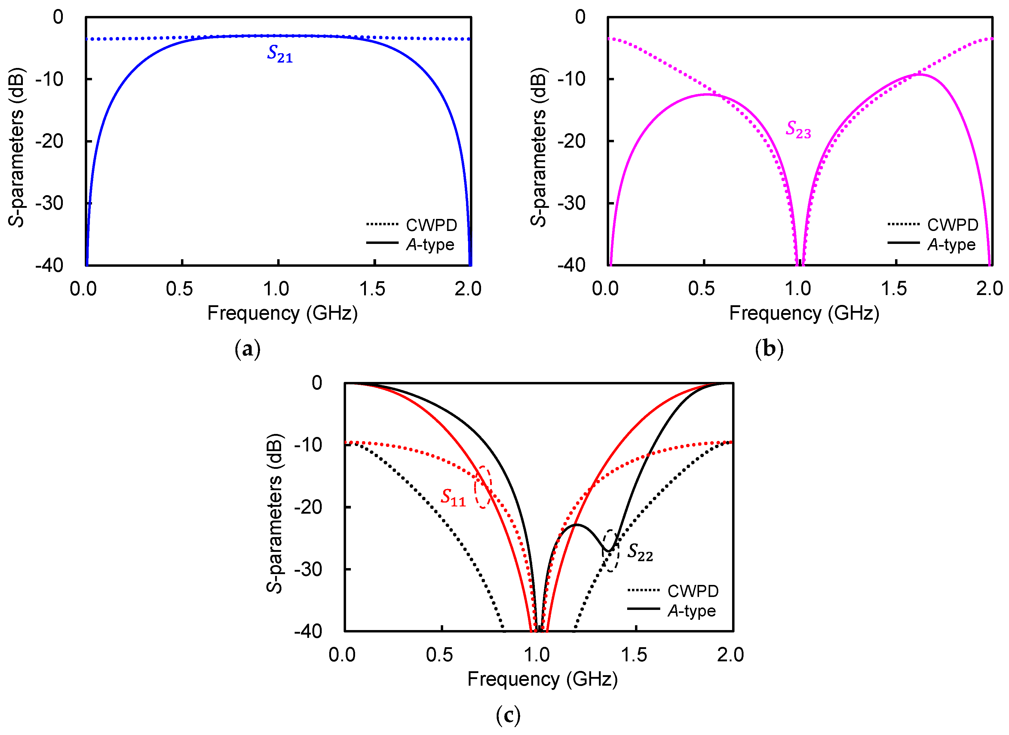
Figure 5 shows the simulation performance of the A-type HS WPD, which is compared with that of the CWPD. As shown in Figure 5a, the A-type HS WPD exhibits a BPF performance in the transmission (), which is in contrast to the CWPD with an all–pass response. This frequency selectivity was due to the presence of the PRSS.

Figure 5.
Simulated performance of designed A–type HS WPD at 1 GHz using PRSS with and 45°. (a) . (b) . (c) and . Solid: A–type, dotted: CWPD.
The CWPD exhibits a good isolation () between the two output ports only at the center frequency, as shown in Figure 5b. In contrast, the A-type HS WPD maintains an isolation of more than 9.3 dB from the dc to 2nd harmonic frequency. That is, the designed A-type HS WPD exhibits perfect isolation at the center frequency, dc, and 2nd harmonic frequencies. This is because the shorted and open stubs in the PRSS provide a short impedance at the dc and 2nd harmonic frequencies, respectively.
The simulated return losses at the input/output ports ( and ) are displayed in Figure 5c. The designed A-type HS WPD shows good impedance matching at the center frequency with a 22% improvement in the fractional bandwidth of a 20-dB input return loss (||) compared to the CWPD.
In summary, the proposed A–type HS WPD utilizing the PRSS effectively allows dc and 2nd harmonic suppression while ensuring both electrical and physical isolation with broad bandwidth.
3.2. Harmonic Suppression Filter Using PRSS
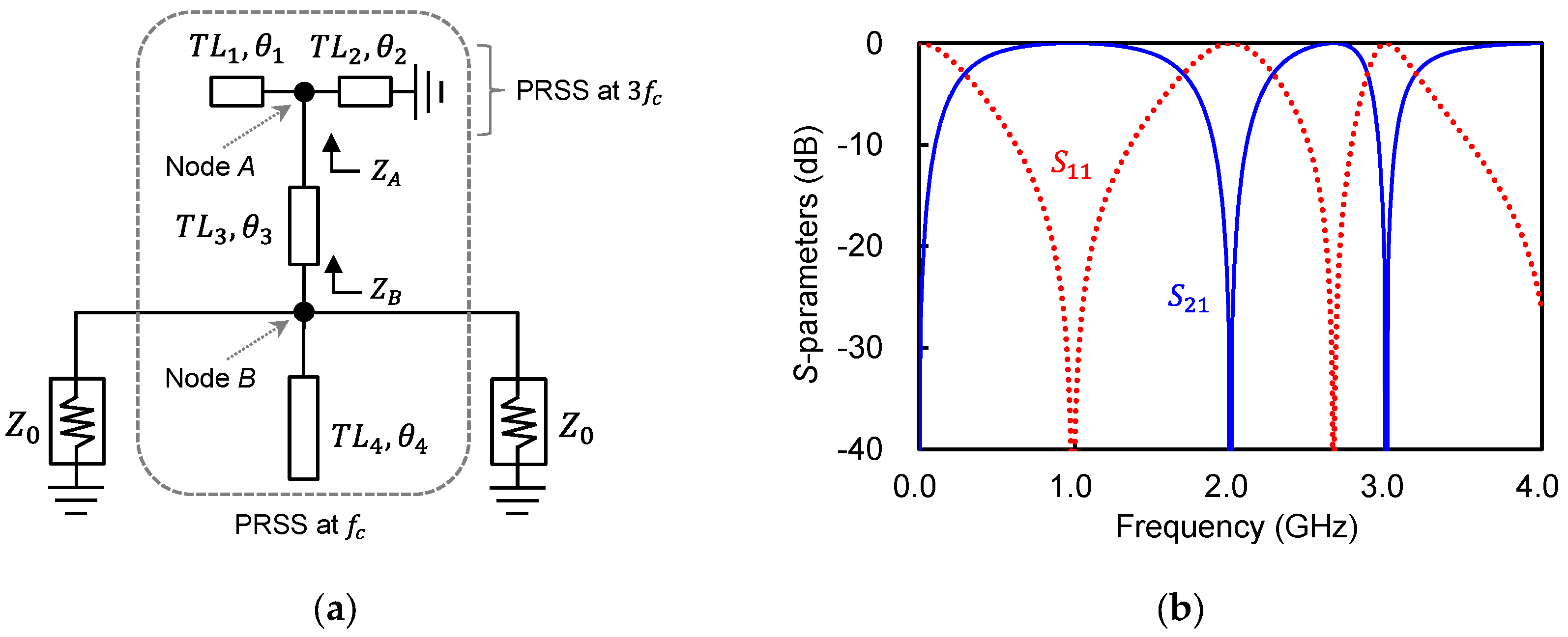
The PRSS can also be utilized to design a 2nd and 3rd harmonic suppression filter, which achieves impedance matching at the fundamental frequency while maintaining a short impedance at the harmonic frequencies. Figure 6a illustrates the configuration of the harmonic suppression filter, which incorporates two PRSSs operating at the fundamental frequency () and three times the fundamental frequency (3).
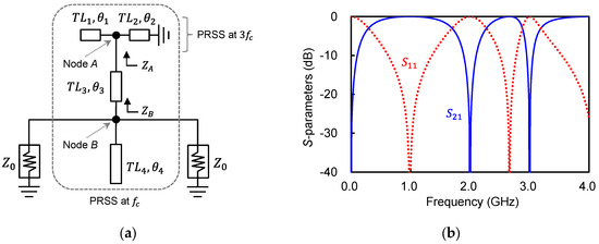
Figure 6.
Harmonic suppression filter incorporating PRSSs. (a) Circuit schematic. (b) Simulated S–parameters of designed harmonic suppression filter at 1 GHz using PRSS with characteristic impedance of 2.
At the fundamental frequency, when the open and shorted stubs ( and ) have an electrical length of 15° with a characteristic impedance of , they produce input impedances of and , respectively, as determined by (1) and (2). Consequently, the input impedance of the parallel combination of open and shorted stubs ( and ) can be approximated as that of the shorted stub, denoted as . If the electrical length of is 30°, is approximately equal to the impedance of the 45° shorted stub at the fundamental frequency. Therefore, when the electrical length of becomes 45°, the circuit in Figure 6a functions as a PRSS at the fundamental frequency, enabling band–pass filtering characteristic.
At the 2nd harmonic frequency, the open stub () with an electrical length of 45° in Figure 6a exhibits a short impedance, effectively shorting node B. This configuration enables the suppression of the 2nd harmonic signal.
At the 3rd harmonic frequency, the open and shorted stubs ( and ) with an electrical length of 15° function as a 45° PRSS, resulting in an open impedance, or . As a result, the with an electrical length of 30° open stub causes a short impedance at node B, indicating the suppression of the 3rd harmonic signal.
Figure 6b illustrates the simulated S–parameters of the harmonic suppression filter, which was designed at a center frequency of 1 GHz using transmission lines with a characteristic impedance of 2. The plot demonstrates that it operates as a BPF at the center frequency while effectively suppressing the 2nd and 3rd harmonic signals, including the signal at dc, where the signals are fully reflected. However, there is a passband between 2nd and 3rd harmonic frequencies. This drawback can be alleviated by decreasing the characteristic impedance of the PRSS, although this may result in a reduced passband bandwidth. As a result, the proposed configuration offers a simple structure and a small number of design variables, making it suitable for creating a BPF with harmonic suppression.
3.3. B-Type HS WPD Using Harmonic Suppression Filter
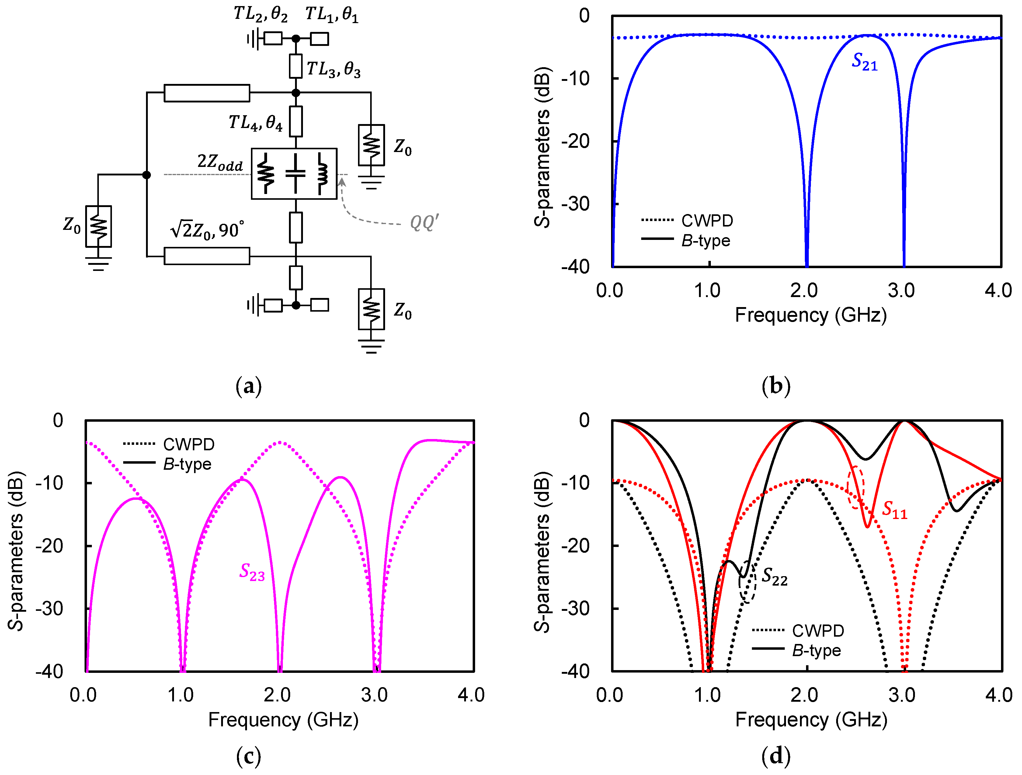
A B–type HS WPD can be designed using the harmonic–suppression filters discussed in the previous section. Figure 7a presents a circuit schematic of the designed B–type HS WPD, where the harmonic suppression filters shown in Figure 6a are incorporated at the output ports. Therefore, the electrical lengths of the harmonic suppression filter are as follows: , , and . It essentially functions as a WPD, providing impedance matching at all ports, equal power division, and almost perfect isolation between the output ports at the center frequency. Additionally, it functions to suppress the dc, 2nd, and 3rd harmonic signals. Similar even- and odd–mode analyses, depicted in Figure 4, can be carried out for this configuration.
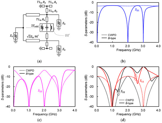
Figure 7.
B–type Harmonic suppressed WPD. (a) Circuit schematic incorporating PRSS at output ports. Simulated S–parameters: (b) . (c) . (d) and . Solid: B–type, dotted: CWPD.
Figure 7b–d depicts the simulated S-parameters of the designed B–type HS WPD at a center frequency of 1 GHz, along with those of the CWPD. The harmonic suppression filters were designed using open and shorted stubs (, , , and ) with a characteristic impedance of , aiming for a wide bandwidth. The isolation network is identical to that used in the A-type HS WPD.
Figure 7b demonstrates that the designed B-type HS WPD exhibits band–pass filtering characteristics with a center frequency of 1 GHz, effectively rejecting signals at dc, 2, and 3. It also provides almost perfect isolation (||) at dc, , 2, and 3, as shown in Figure 7c, achieving isolation greater than 9.0 dB from dc to 3.2 GHz. The simulated || and || are not perfect but less than −40.5 dB at the fundamental frequency, as depicted in Figure 7d, whereas it is 0 dB at the 2nd and 3rd harmonic frequencies.
As a result, the designed B-type HS WPD utilizing PRSSs successfully incorporated the essential functionalities of a WPD at the fundamental frequency. Furthermore, it offers additional features including dc suppression and harmonic suppression, along with physical port separation. Despite its added functionalities, this multifunctional power divider maintains a straightforward design and a compact size.
4. Experimental Results
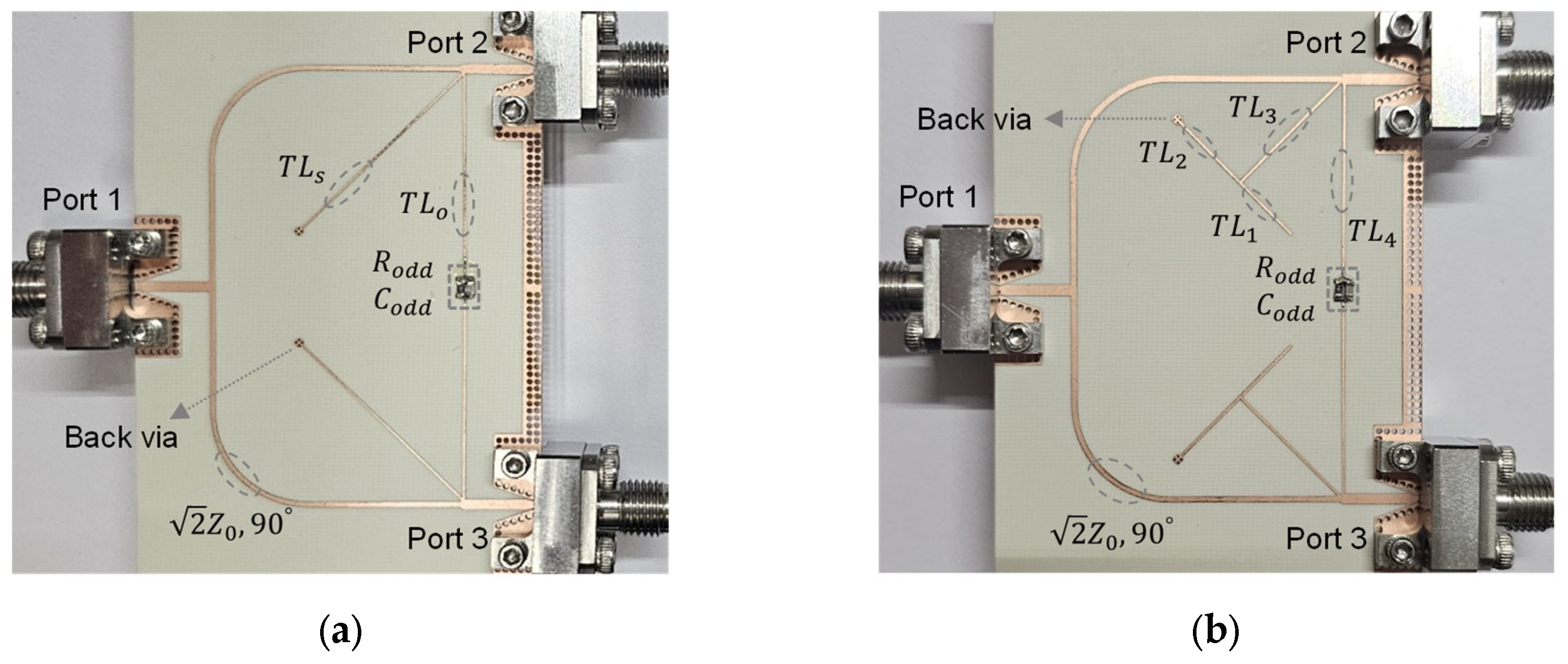
The A- and B-type HS WPD were designed as described in the previous section, and fabricated using 20 mil–thick dielectric substrates with a dielectric constant of 3.55 (Rogers RO4003C). To accurately determine the dimensions of the microstrip lines, an electromagnetic simulation was performed using Keysight’s Advanced Design System (ADS). The fabricated A- and B-type HS WPD are shown in Figure 8, and their sizes are 3.28 cm × 4.87 cm (0.18 × 0.27 and 3.43 cm × 4.47 cm (0.19 × 0.25 , respectively, where is the guided wavelength at center frequency. End–launch connectors were employed at each port for the measurement, and it was observed that the two output ports were physically separated, owing to the inclusion of the PRSSs. The shorted stubs in the PRSSs are implemented using backside vias. However, in the isolation network, a 400-fF capacitor could not be obtained as a discrete component; therefore a 300-fF capacitor was used as a substitute. This substitution led to slight discrepancies between the measured and simulated output return losses and isolation performance. The S–parameter measurements were conducted using a vector network analyzer (C4220 by Copper Mountain Technologies).
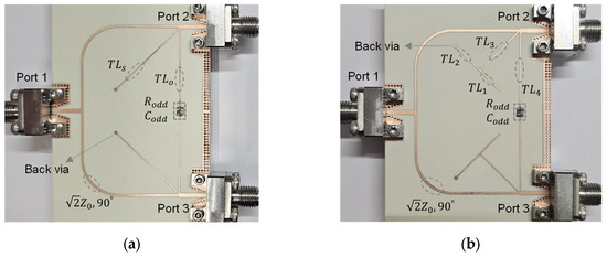
Figure 8.
Photograph of fabricated harmonic suppressed Wilkinson power dividers (a) A-type and (b) B-type.
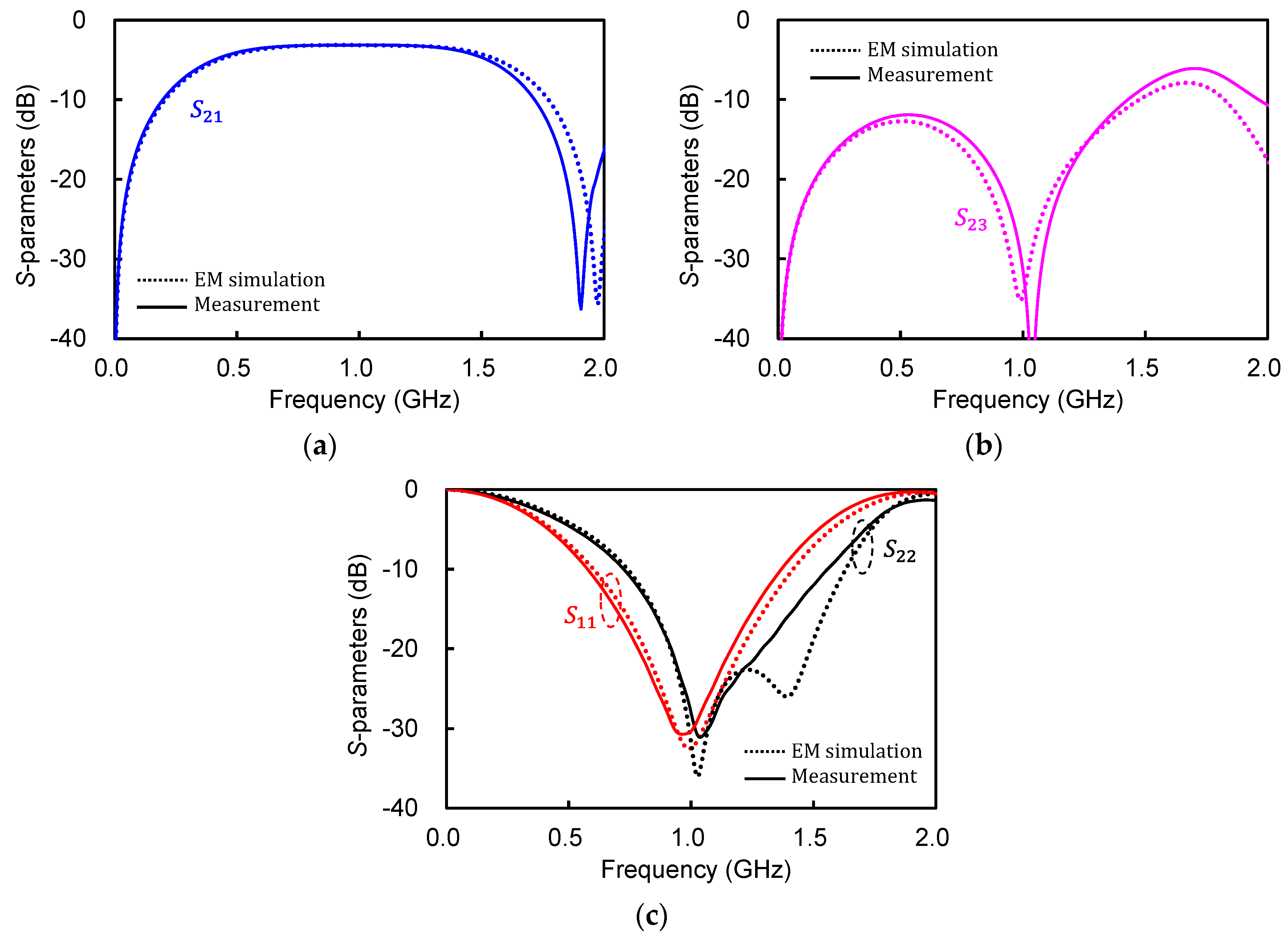
Figure 9 shows the measured S-parameters of the fabricated A-type HS WPD compared to the EM simulation results. In Figure 9a, the measured || exhibits a bandpass filtering characteristic with a 3-dB bandwidth as large as 130% (0.335–1.59 GHz) owing to the proposed PRSS. The insertion loss (−20log||) was 3.2 dB at 1 GHz. There is a deviation in the null frequency of || compared to the EM simulation, which is caused by the additional lines used to connect the RC components in the isolation network. Figure 9b shows the measured isolation (−20log||), which is 31.4 dB at 1 GHz and remains greater than 6.1 dB from dc to 2 GHz. The measured input and output return losses (−20log|| and −20log||) were 30.3 and 28.1 dB, respectively, at 1 GHz, as depicted in Figure 9c.

Figure 9.
Measurement results of fabricated A–type HS WPD. (a) . (b) . (c) and . Solid: measurements, dotted: EM simulations.
Figure 10 presents the measured S–parameters of the fabricated B-type HS WPD. As shown in Figure 10a, the insertion loss is 3.2 dB at 1 GHz, and the 3 dB bandwidth is 129% (0.345–1.595 GHz), which is similar to that of the A–type HS WPD. The harmonic suppression capability of the B–type HS WPD is evident, as it exhibits high insertion loss of 21.0 dB and 25.8 dB at 2 and 3 GHz, respectively. Figure 10b illustrates the measured isolation performance, which was 29.2 dB at 1 GHz. It also exhibits a relatively good isolation (>8.7 dB) over a wide frequency range from 100 kHz to 3.35 GHz. In this study, a parallel resistor and capacitor configuration was adopted for the isolation network, considering the parasitic effects of the fabrication. The simulation showed that a series configuration can achieve better isolation over a broader bandwidth. The measured input and output return loss is 27.9 dB and 24.6 dB, respectively, at 1 GHz, as shown in Figure 10c. There is a slight discrepancy between the measured and simulated results in Figure 9 and Figure 10, which can be attributed to the use of different capacitances (300 fF instead of 400 fF) and the parasitic components of the surface–mounted device (SMD) capacitor.
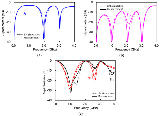
Figure 10.
Measurement results of fabricated B–type HS WPD. (a) . (b) . (c) and . Solid: measurements, dotted: EM simulations.
Table 2 provides a comprehensive performance comparison of the reported PDs. There have been several publications on PDs with the band–pass characteristics and physical port separation, such as [8,11,15]. In contrast, the proposed B–type HS WPD demonstrated the widest bandwidth (129%) with a low insertion loss of 3.2 dB at the fundamental frequency. Additionally, it exhibited good harmonic suppression at both the 2nd and 3rd harmonic frequencies. This remarkable performance can be attributed to the simplicity of the circuit topology in the proposed PRSS, which involves fewer design variables and a compact size compared with other publications.
Table 2.
Performance comparison of reported power dividers.
5. Conclusions
In this paper, we proposed and analyzed parallel–resonant shunt stubs. We investigated their characteristics, such as bandpass filtering and harmonic suppression, based on the derived resonance conditions. We also analyzed the impact of the characteristic impedance and electrical length of the stubs on performance. Additionally, we utilized the parallel resonant shunt stubs to design the HS FWPD. These PDs not only provide bandpass filtering and harmonic suppression but also offer physical separation of the output ports. At the same time, they maintained the performance of the CWPDs at the fundamental frequency. The designed PDs were fabricated and their performances were experimentally verified. The HS FWPD proposed in this work, which offers excellent performance and multiple functions within a compact size, is anticipated to find applications in various microwave systems. Future research could explore the use of multiple PRSSs to enhance the stopband performance.
Author Contributions
Conceptualization, Y.J. and J.J.; methodology, Y.J. and J.J.; software, Y.J.; validation, Y.J. and J.J.; formal analysis, Y.J. and J.J.; investigation, Y.J.; resources, Y.J.; data curation, Y.J.; writing-original draft preparation, Y.J. and J.J.; writing-review and editing, J.J.; visualization, Y.J.; supervision, J.J.; project administration, J.J.; funding acquisition, J.J. All authors have read and agreed to the published version of the manuscript.
Funding
This work was supported in part by the National Research Foundation (NRF), Korea, under project BK21 FOUR and in part by National R&D Program through the National Research Foundation of Korea (NRF) funded by Ministry of Science and ICT (2021M3H2A1038042).
Institutional Review Board Statement
Not applicable.
Informed Consent Statement
Not applicable.
Data Availability Statement
The data presented in this study are available on request from the corresponding author.
Conflicts of Interest
The authors declare no conflicts of interest.
References
- Wilkinson, E.J. An N-Way Hybrid Power Divider. IEEE Trans. Microw. Theory Tech. 1960, 8, 116–118. [Google Scholar] [CrossRef]
- Kim, J.; Jeon, S.; Kim, M.; Urteaga, M.; Jeong, J. H-Band Power Amplifier Integrated Circuits Using 250-nm InP HBT Technology. IEEE Trans. Terahertz Sci. Technol. 2015, 5, 215–222. [Google Scholar] [CrossRef]
- Chieh, J.-C.S.; Yeo, E.; Farkouh, R.; Castro, A.; Kerber, M.; Olsen, R.B.; Merulla, E.J.; Sharma, S.K. Development of Flat Panel Active Phased Array Antennas Using 5G Silicon RFICs at Ku- and Ka-Bands. IEEE Access 2020, 8, 192669–192681. [Google Scholar] [CrossRef]
- Feghhi, R.; Joodaki, M. Odd-Mode Instability Analysis of fT-Doubler Hybrid Power Amplifiers Based on GaN-HEMT. IEEE Trans. Circuits Syst. II Express Briefs 2021, 68, 1193–1197. [Google Scholar]
- Lotfi, S.; Roshani, S.; Roshani, S.; Gilan, M.S. Wilkinson Power Divider with Band-pass Filtering Response and Harmonics Suppression Using Open and Short Stubs. Frequenz 2020, 74, 169–176. [Google Scholar] [CrossRef]
- Li, Y.C.; Xue, Q.; Zhang, X.Y. Single- and Dual-Band Power Dividers Integrated with Bandpass Filters. IEEE Trans. Microw. Theory Tech. 2013, 61, 69–76. [Google Scholar] [CrossRef]
- Deng, P.-H.; Dai, L.-C. Unequal Wilkinson Power Dividers with Favorable Selectivity and High-Isolation Using Coupled-Line Filter Transformers. IEEE Trans. Microw. Theory Tech. 2012, 60, 1520–1529. [Google Scholar] [CrossRef]
- Xu, K.D.; Bai, Y.; Ren, X.; Xue, Q. Broadband Filtering Power Dividers Using Simple Three-Line Coupled Structures. IEEE Trans. Compon. Packag. Manuf. Technol. 2019, 9, 1103–1110. [Google Scholar] [CrossRef]
- Liu, Y.; Sun, S.; Zhu, L. Design of n-Way Wideband Filtering Power Dividers with Good Port–Port Isolation. IEEE Trans. Microw. Theory Tech. 2021, 69, 3298–3306. [Google Scholar] [CrossRef]
- Chen, C.-J.; Ho, Z.-C. Design Equations for a Coupled-Line Type Filtering Power Divider. IEEE Microw. Wirel. Compon. Lett. 2017, 27, 257–259. [Google Scholar] [CrossRef]
- Chen, M.-T.; Tang, C.-W. Design of the Filtering Power Divider with a Wide Passband and Stopband. IEEE Microw. Wirel. Compon. Lett. 2018, 28, 570–572. [Google Scholar] [CrossRef]
- Zhang, G.; Wang, X.; Hong, J.-S.; Yang, J. A High-Performance Dual-Mode Filtering Power Divider with Simple Layout. IEEE Microw. Wirel. Compon. Lett. 2018, 28, 120–122. [Google Scholar] [CrossRef]
- Wang, D.; Guo, X.; Wu, W. Wideband Unequal Power Divider with Enhanced Power Dividing Ratio, Fully Matching Bandwidth, and Filtering Performance. IEEE Trans. Microw. Theory Tech. 2022, 70, 3200–3212. [Google Scholar] [CrossRef]
- Song, K.; Fan, M.; Zhang, F.; Zhu, Y.; Fan, Y. Compact Triple-Band Power Divider Integrated Bandpass-Filtering Response Using Short-Circuited SIRs. IEEE Trans. Compon. Packag. Manuf. Technol. 2017, 7, 1144–1150. [Google Scholar] [CrossRef]
- Lee, B.; Nam, S.; Lee, J. Filtering Power Divider with Reflectionless Response and Wide Isolation at Output Ports. IEEE Trans. Microw. Theory Tech. 2019, 67, 2684–2692. [Google Scholar] [CrossRef]
- Zhang, X.Y.; Wang, K.-X.; Hu, B.-J. Compact Filtering Power Divider with Enhanced Second-Harmonic Suppression. IEEE Microw. Wirel. Compon. Lett. 2013, 23, 483–485. [Google Scholar] [CrossRef]
- Wang, Y.; Zhang, X.-Y.; Liu, F.-X.; Lee, J.-C. A Compact Bandpass Wilkinson Power Divider with Ultra-Wide Band Harmonic Suppression. IEEE Microw. Wirel. Compon. Lett. 2017, 27, 888–890. [Google Scholar] [CrossRef]
- Woo, D.-J.; Lee, T.-K. Suppression of Harmonics in Wilkinson Power Divider Using Dual-Band Rejection by Asymmetric DGS. IEEE Trans. Microw. Theory Tech. 2005, 53, 2139–2144. [Google Scholar]
- Yang, J.; Gu, C.; Wu, W. Design of Novel Compact Coupled Microstrip Power Divider with Harmonic Suppression. IEEE Microw. Wirel. Compon. Lett. 2008, 18, 572–574. [Google Scholar] [CrossRef]
- Kumar, M.; Islam, S.N.; Sen, G.; Kumar Parui, S.; Das, S. Harmonic Suppressed Wilkinson Power Divider with Filtering Characteristic for GSM Application. In Proceedings of the 2018 IEEE MTT-S International Microwave and RF Conference (IMaRC), Kolkata, India, 28–30 November 2018; pp. 1–3. [Google Scholar]
- Lin, C.-M.; Su, H.-H.; Chiu, J.-C.; Wang, Y.-H. Wilkinson Power Divider Using Microstrip EBG Cells for the Suppression of Harmonics. IEEE Microw. Wirel. Compon. Lett. 2007, 17, 700–702. [Google Scholar] [CrossRef]
- Yi, K.-H.; Kang, B. Modified Wilkinson Power Divider for nth Harmonic Suppression. IEEE Microw. Wirel. Compon. Lett. 2003, 13, 178–180. [Google Scholar]
- Jamshidi, M.; Lalbakhsh, A.; Lotfi, S.; Siahkamari, H.; Mohamadzade, B.; Jalilian, J. A neuro-based approach to designing a Wilkinson power divider. Int. J. RF Microw. Comput.-Aided Eng. 2020, 30, e22091. [Google Scholar] [CrossRef]
- Karimi, G.; Menbari, S. A Novel Wilkinson Power Divider Using Lowpass Filter with Harmonics Suppression and High Fractional Bandwidth. Microelectron. J. 2018, 71, 61–69. [Google Scholar] [CrossRef]
- Jedkare, E.; Shama, F.; Sattari, M.A. Compact Wilkinson Power Divider with Multi-Harmonics Suppression. AEU Int. J. Electron. Commun. 2020, 127, 153436. [Google Scholar] [CrossRef]
- Moloudian, G.; Soltani, S.; Bahrami, S.; Buckley, J.L.; O’flynn, B.; Lalbakhsh, A. Design and fabrication of a Wilkinson power divider with harmonic suppression for LTE and GSM applications. Sci. Rep. 2023, 13, 4246. [Google Scholar] [CrossRef] [PubMed]
- Choe, W.; Jeong, J. Compact Modified Wilkinson Power Divider with Physical Output Port Isolation. IEEE Microw. Wirel. Compon. Lett. 2014, 24, 845–847. [Google Scholar] [CrossRef]
- Choe, W.; Jeong, J. N-Way Unequal Wilkinson Power Divider with Physical Output Port Separation. IEEE Microw. Wirel. Compon. Lett. 2016, 26, 243–245. [Google Scholar] [CrossRef]
- Chang, T.-J.; Huang, T.-J.; Hsu, H.-T. A New Design of Wilkinson Power Divider Using Radial Stubs Featuring Size Reduction and Bandwidth Enhancement with Physical Isolation. In Proceedings of the 2017 IEEE 18th Wireless and Microwave Technology Conference (WAMICON), Cocoa Beach, FL, USA, 24–25 April 2017; pp. 1–4. [Google Scholar]
- Cheng, K.-K.M.; Ip, W.-C. A Novel Power Divider Design with Enhanced Spurious Suppression and Simple Structure. IEEE Trans. Microw. Theory Tech. 2010, 58, 3903–3908. [Google Scholar] [CrossRef]
- Trantanella, C.J. A Novel Power Divider with Enhanced Physical and Electrical Port Isolation. In Proceedings of the 2010 IEEE MTT-S International Microwave Symposium, Anaheim, CA, USA, 23–28 May 2010; p. 1. [Google Scholar]
- Wang, X.; Sakagami, I.; Mase, A.; Ichimura, M. Wilkinson Power Divider with Complex Isolation Component and Its Miniaturization. IEEE Trans. Microw. Theory Tech. 2014, 62, 422–430. [Google Scholar] [CrossRef]
- Horst, S.; Bairavasubramanian, R.; Tentzeris, M.M.; Papapolymerou, J. Modified Wilkinson Power Dividers for Millimeter-Wave Integrated Circuits. IEEE Trans. Microw. Theory Tech. 2007, 55, 2439–2446. [Google Scholar] [CrossRef]
- Antsos, D.; Crist, R.; Sukamto, L. A Novel Wilkinson Power Divider with Predictable Performance at K and Ka-band. In Proceedings of the 1994 IEEE MTT-S International Microwave Symposium Digest, San Diego, CA, USA, 23–27 May 1994; Volume 2, pp. 907–910. [Google Scholar]
- Jang, Y.; Jeong, J. Modified Wilkinson Power Divider with Resonating Stubs for Physical Isolation of Output Ports. In Proceedings of the 2022 19th International SoC Design Conference (ISOCC), Gangneung-si, Republic of Korea, 19–22 October 2022; pp. 380–381. [Google Scholar]
- Pozar, D.M. Microwave Engineering; Wiley: Hoboken, NJ, USA, 2009. [Google Scholar]


Disclaimer/Publisher’s Note: The statements, opinions and data contained in all publications are solely those of the individual author(s) and contributor(s) and not of MDPI and/or the editor(s). MDPI and/or the editor(s) disclaim responsibility for any injury to people or property resulting from any ideas, methods, instructions or products referred to in the content. |
© 2024 by the authors. Licensee MDPI, Basel, Switzerland. This article is an open access article distributed under the terms and conditions of the Creative Commons Attribution (CC BY) license (https://creativecommons.org/licenses/by/4.0/).