Article

Considerations on the Development of High-Power Density Inverters for Highly Integrated Motor Drives

1
Department of Electrical and Electronic Engineering, University of Nottingham Ningbo China, Ningbo 315100, China
2
Department of Electrical Engineering, University of Malta, MSD 2080 Msida, Malta
*
Author to whom correspondence should be addressed.
Electronics 2024, 13(2), 355; https://doi.org/10.3390/electronics13020355
Submission received: 6 December 2023 / Revised: 31 December 2023 / Accepted: 10 January 2024 / Published: 14 January 2024

Abstract

:
In transportation electrification, power modules are considered the best choice for power switches to build a high-power inverter. Recently, several studies have presented prototypes that use parallel discrete MOSFETs and show similar overall output capabilities. This paper aims to compare the maximum output power and losses of inverters with different types (surface-mounted, through-hole-mounted and power modules) of commercially available switching devices, and, therefore, discuss the theoretical boundaries of each technology. The numerical analysis relies on detailed power loss and thermal models, with adjustments made for gate current and realistic parameters of the cooling system. The analysis includes two case studies with different targets, including minimum dimensional characteristics and maximum output power. The results demonstrate that discrete MOSFETs can provide improved capabilities in contrast to power modules under certain conditions.

1. Introduction

An electrical drive is a sub-system on which significant efforts are pushed towards the electrification of transportation, and its crucial role is known throughout all sectors of industry. As a result, electrical drives are able to compete with internal combustion engines or gear transmission systems in terms of operational values. While electric drive technology has made remarkable steps forward in the last few decades, many challenges remain. These include the implementation of new functionalities, higher power density and system reliability and better components availability [1]. The concept of motor integration is one of the central themes to all the above. To achieve higher system operational requirements, the physically integrated approach coupled with higher speeds and new materials is critical [2]. Moreover, industry-oriented studies [3,4] have stated that harsh operating conditions may introduce further technical challenges for electrical drivers in some Electric Vehicle (EV) applications.
The development of a power converter for an integrated motor drive with an output power ranging from several dozens to hundreds of kW often requires moving away from traditional patterns and using unconventional design methods. Several distinct approaches are used to achieve the desired power level. A group of researchers applied custom-designed power modules to avoid the temperature limitations of the package’s materials [5,6,7]. Such modules use a ceramic substrate and silicon carbide (SiC) dies without a plastic cover; therefore, the maximum temperature is limited only by the thermal capability of the SiC, solder and a baseplate. A clear disadvantage of this approach is that the exploitation of the design in research or industry is difficult, and complicated equipment is required to produce custom SiC modules. Researchers do have to choose the serially produced SiC products in order to obtain a converter that can be repeated or manufactured.
Another approach commonly used to achieve the required power is to exploit commercial SiC power modules [8,9,10,11,12], as they are featured with the best thermal performance and a high current rating among other serially produced components. Power modules are convenient and effective means of building a power converter. On the other hand, their heavy weight and bulky dimensions (see Figure 1) might cause difficulties with the layout if the project demands a specific complex housing shape.
The maintenance and modernization of the converter with power modules might also be challenging due to the large variety of their shapes and terminal locations; examples of modules are shown in Figure 2. The transition to other series or manufacturers of power modules mostly causes the redesign of the inverter’s other components.
Alternative power electronics designs based on discrete components can provide an optimal solution with higher flexibility to operate a variety of standardized power switching devices. A number of studies [17,18,19,20,21] demonstrated that high power inverters with parallel SiC MOSFETs can prove their competitiveness in this application field. However, it remains unclear what the possible output current and power that discrete components can reach, as many factors may affect the performance.
This paper aims to demonstrate the capabilities of power modules and through-hole (THT) and surface-mounted (SMT) discrete SiC MOSFETs under the same operating conditions across a range of ambient/cooling temperatures. The results might assist engineers and researchers to obtain a more comprehensive picture of theoretical power boundaries and features of different MOSFET packages. A thermal model with a losses analysis utilizes datasheet information about temperature and drain current-dependent parameters to obtain accurate results. A large number of publications (for instance, [22,23,24]) have applied a losses thermal model for the needs of optimization within a single design or topology comparison. However, these papers did not cover many MOSFET types and did not focus on the evaluation of maximum output power. Moreover, this study considers the external gate resistance as an input parameter for analysis due to the limitation of the gate driver’s output current. In order to address the interests of integration-oriented studies, the analysis also includes occupied area, mass and volume parameters to assess the effect of different packages on the dimensions and weight of the inverter.
The rest of the paper is organized as follows. Section 2 describes the proposed thermal model and selection criteria of MOSFETs, while Section 3 demonstrates the analysis of the first case study with a fixed output power. The results of the second case study with maximum output power are mentioned in Section 4, which is followed by the discussion in Section 5.

2. Materials and Methods
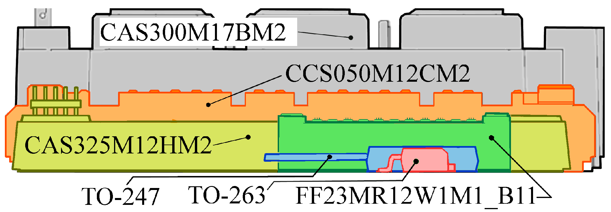
2.1. Power Switches

Three package types of semiconductor power switches were examined in this study as a potential choice for the role of the Integrated Motor Drive (IMD) power switch.

2.1.1. Discrete SiC MOSFETs

SiC MOSFETs are presented on the market in a large variety of drain current capabilities and blocking voltages to help designers balance between performance, power losses and economic reasonability. Several manufacturers of SiC MOSFET in SMT and THT packages have started production since its first appearance in the mid-2010s. Devices with the best figures for the drain current are included in the analysis to demonstrate the best achievable capabilities. Maximum blocking drain voltage of selected MOSFETs does not exceed 1200 V to target typical requirements for typical aircraft bus voltage and EV traction drivers.
In detail, important characteristics of many up-to-date commercially available SMT SiC MOSFETs are presented in Table A1. Although TO-263-7 is the oldest and the most popular package type, developers introduce smaller packages to reduce height and the chip area targeting embedded electronics and highly integrated solutions.
All THT MOSFETs have TO-247-4 package (or its variants) due to reduced power losses by comparison with the earlier 3-pin design of TO-247, where the gate driver circuit uses the source pin. In total, 9 types by 7 companies were selected, and their parameters are presented in Table A2.
The production of SiC MOSFETs is an active and dynamically developing industry with both gradual enhancement of existing technologies and the testing of new approaches. Updated versions of semiconductor devices emerge regularly and extend the performance boundaries of power electronics.

2.1.2. Power Modules

Power modules contain semiconductor switching devices with large die areas or parallel dies to achieve high values for output current and level up power density. Advanced technological processes enable the utilization of materials with thermal conductivity while standardized procedures maintain the repeatability of characteristics and predictable reliability.
The parallel connection of semiconductor power modules in a single switching unit is not a common practice due to difficulties with current sharing and stability without additional measures. Relatively large distances between terminals lead to high inductances in gate traces and high-power buses and, therefore, disturbance of gate signals and current inequality. Detailed parameters of power modules included in the consideration are listed in Table A3.

2.2. Losses Calculation and Thermal Model

If high-power density is the primary goal, power electronics designers must operate power switches at the maximum of their thermal capabilities. Maintaining the junction temperature below the rated value requires careful evaluation of the MOSFET’s operating point and heat dissipation. In order to minimize weight and dimensions, the number of MOSFETs should be kept to a minimum.
Some assumptions were made to simplify the calculations:
  • All parallel devices share phase drain current in equal parts;
  • Dead-time-related losses (difference in conduction losses between diodes and MOSFETs) were not included;
  • Diode partial current sharing in 3rd quadrant was not considered in this model; therefore, diode’s conduction losses were not included in calculations.
Maximum and RMS drain currents of a device ( I D S   m a x and I D S r m s respectively) were calculated as follows:
I D S   r m s = I G R   r m s   N P P G = I P H   m a x 2 N P P G ,   I D S   m a x = I P H   m a x N P P G
where N P P G is the number of devices per group, I G R   r m s   is the group RMS current and I P H   m a x is the maximum phase current.
The power losses of a MOSFET ( P M O S F E T ) are calculated as the sum of conduction ( P C ) and switching power losses ( P S W ). Considering sine PWM modulation, switching losses can be expressed through their maximum value of a cycle:
P M O S F E T = P C + P S W = I D S   r m s 2 · R d s   o n T J , I D S   m a x + F s w E S W   t o t   r a t e d π K T J · K V D C · K I D S · K R G
where E S W   t o t r a t e d is the total switching losses under the rated conditions that are specified in the datasheet, K T J   is the junction temperature ( T J ) scaling coefficient, K V D C is the input DC-link voltage ( V d c ) scaling coefficient, K I D S is the maximum drain current ( I D S   m a x ) scaling coefficient and K R G is the scaling coefficient of gate external resistance ( R g   e x t ). Parameters, measured or specified at the rated operating point (selected by manufacturer for the measurement of switching energy losses), have an index “rated” in their description. Reverse recovery losses are already included in total switching losses because manufacturers use the same type of MOSFET as a body diode to obtain experimental values specified in the datasheet.
In the calculation model the drain-source channel resistance R d s   o n depends on T J and I D S   m a x :
R d s   o n T J ,   I D S   m a x = R d s   o n 25 1 + K R T J T J T J   L T ·   K R I ( I D S   m a x ) K R T J = R n d s   o n   T J   H T 1 T J   H T T J   L T ,   K R I ( I D S   m a x ) = A R I · I D S   m a x + B R I R d s   o n 25
where R d s   o n 25 is the drain-source channel resistance at 25 °C, R n d s   o n   T J   H T is the normalized value (divided by R d s   o n 25 ) of MOSFET active resistance under high temperature T J   H T = T J   m a x and T J   L T is the maximum junction temperature, where R d s   o n is close to R d s   o n 25 . Values of A R I and B R I are obtained at the datasheet for the current range 20 A–70 A using linear approximation with acceptable error. Polynomial approximation might be used to follow the non-linear curve for higher drain current.
The shapes of the curves for different parameters vary significantly, so linear, quadratic and power approximations were selected to calculate coefficients:
K V D C V D C = V D C V D C   r a t e d A V D C ;   K I D S ( I D S   m a x ) = A I D S · I D S   m a x 2 + B I D S · I D S   m a x + C I D S E S W   t o t   r a t e d K T J ( T J ) = A T J · T J + B T J E S W   t o t   r a t e d ,       K R G ( R g   e x t ) = A R G · R g   e x t + B R G E S W   t o t   r a t e d ,  
where A x , B x and C x are parameters extracted from MOSFET’s datasheet.
In single MOSFET operations, a gate driver’s output current does not affect the performance of MOSFET due to the high current capabilities of recently developed gate drivers. The most popular maximum value of the output current for a single chip is approximately 30 A, so this value was also the maximum total gate current for analysis. In the analysis t r i s e (target value is 20 ns) determines the initial value of R g   e x t as it might be important for Electromagnetic Interference (EMI) characteristics of the inverter [25], although gate driver current might be used as an input parameter. At the same time, the possible minimum value R g   e x t   m i n in the analysis was determined using the minimum value of R g   e x t mentioned in datasheet to increase accuracy of calculations.
The relationship between the total maximum gate current I G T o t a l and the number of parallel transistors can be expressed as follows:
I G t o t a l = N P P G V G D M a x V G D M i n   R g   i n n e r + R g   e x t 30   A
Total gate current I G t o t a l increases with the number of parallel devices in a group and might reach the limit at some point. Further increase in the number of devices leads to an increase in gate resistance R g   e x t in order to maintain the current at the same level.
For some devices, high inner resistance R g   i n n e r and significant value of gate-drain charge Q g d does not allow a driver to charge C g d fast enough to reach the initial value of t r i s e . For such devices, the initial value of external gate resistance R g   e x t is set to R g   e x t   m i n . Thus, external resistor R g   e x t for each group of MOSFETs was calculated with respect to the value of gate current:
R g   e x t = N P P G V G D M a x V G D M i n               I G t o t a l M A X R g   i n n e r ,                 i f   I G t o t a l = 30   A t r i s e   V G D M a x V G D M i l l Q g d R g   i n n e r ,     i f   I G t o t a l < 30   A R g   e x t   m i n , i f     I G t o t a l < 30   A   a n d   t r i s e   V G D M a x V G D M i l l Q g d < R g   i n n e r R g   e x t   m i n ,                     i f   R g   e x t   m i n > R g   e x t
The final value R g   e x t was used to calculate the coefficient K R G for switching losses.
Although datasheets for most modern MOSFETs contain all the necessary information, documents for older MOSFETs might miss some plots or figures. In that case, default values selected using simplified losses equations were used in the calculation (values are listed in Table 1).
The junction temperature of a device consists of the ambient temperature T a m b , temperature drop between MOSFET’s case and junction T j c a s e and temperature drop between the case and coolant T c a s e h s :
T j = T c a s e h s + T j c a s e + T a m b = P M O S F E T Θ j c + Θ c h s + 1 S P C B A R E A h C P + T a m b , Θ c h s = Θ T I M ,     f o r   p o w e r   m o d u l e s Θ I n s u l a t i o n   p a d + Θ T I M ,     f o r   T H T   c o m p o n e n t s Θ P C B + Θ T I M ,     f o r   S M T   c o m p o n e n t s
where S h s is the area of the thermal pad or the baseplate of a device divided by the number of switching groups inside the package (assuming that heat evenly spreads across the baseplate) and Θ c h s is the total thermal resistance of layers between the case and the heat sink. A traditional structure with indirect cooling of power modules was selected for comparison analysis. The thermal model of THT components implies that heat is transferred through a thermally conductive insulation pad (mica + thermal grease), and for SMT components Insulated Metal Substrate (IMS) was selected as a reference for Θ c h s values with Printed Circuit Board (PCB) and Thermal Interface Material (TIM) parameters.
As the inverter’s area is one of the targets, keeping a small distance between devices was reasonable. For analysis, the distance between two MOSFETs was 2 mm, and each device used an extra 1 mm layer of copper on each side of its thermal pad to spread the heat. Other important parameters of thermal interface materials and calculated values of MOSFET’s thermal resistances are stated in Table 2.
The volume (V) and the area (A) of a power module were calculated based on their dimensions from datasheets. The area and the volume of SMT and THT devices included extra space (values are presented in Figure 3) for connections of power buses and gate circuits:
A S M T = 6 N P P G W i d t h + 2   m m + 2   m m L e n g t h + 10   m m ,
A T H T = 6 N P P G W i d t h + 2   m m + 2   m m L e n g t h + 10   m m ,
V S M T = A S M T H e i g h t + 7   m m + 2   m m ,   V P T H = A P T H H e i g h t + 7   m m
The high junction temperature T j affects many parameters of MOSFET and causes an increase in both conduction and switching losses, which, in turn, increase the generated heat and junction temperature. A multi-iteration algorithm was used to recalculate temperature-dependent coefficients and obtain accurate results for the whole range of junction temperature (see Figure 4). The initial junction temperature was equal to the coolant temperature and was updated every cycle until the difference between the two steps is less than 2 °C. This method helped to detect possible thermal runaway and evade overestimation of conductive losses due to too high expectation of R d s   o n . All combinations that led to excessive junction temperature were excluded from the analysis.
The total weight W S M T of an inverter with SMT components includes the weight of a 2 mm aluminum baseboard as they cannot be used without a heat spreader and can be calculated as
W S M T = 6 N P P G W p a r t + A S M T · 0.2   c m · 2.7 g c m 2
where W p a r t is the weight of the single discrete element according to its datasheet.

3. Performance Analysis

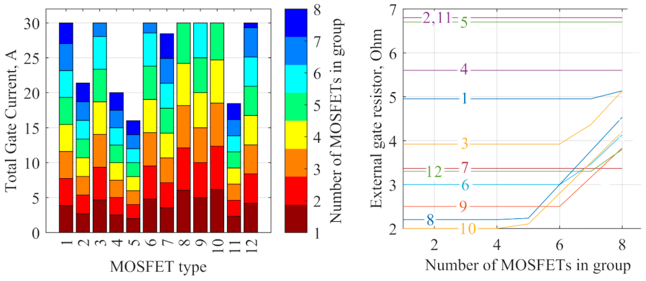
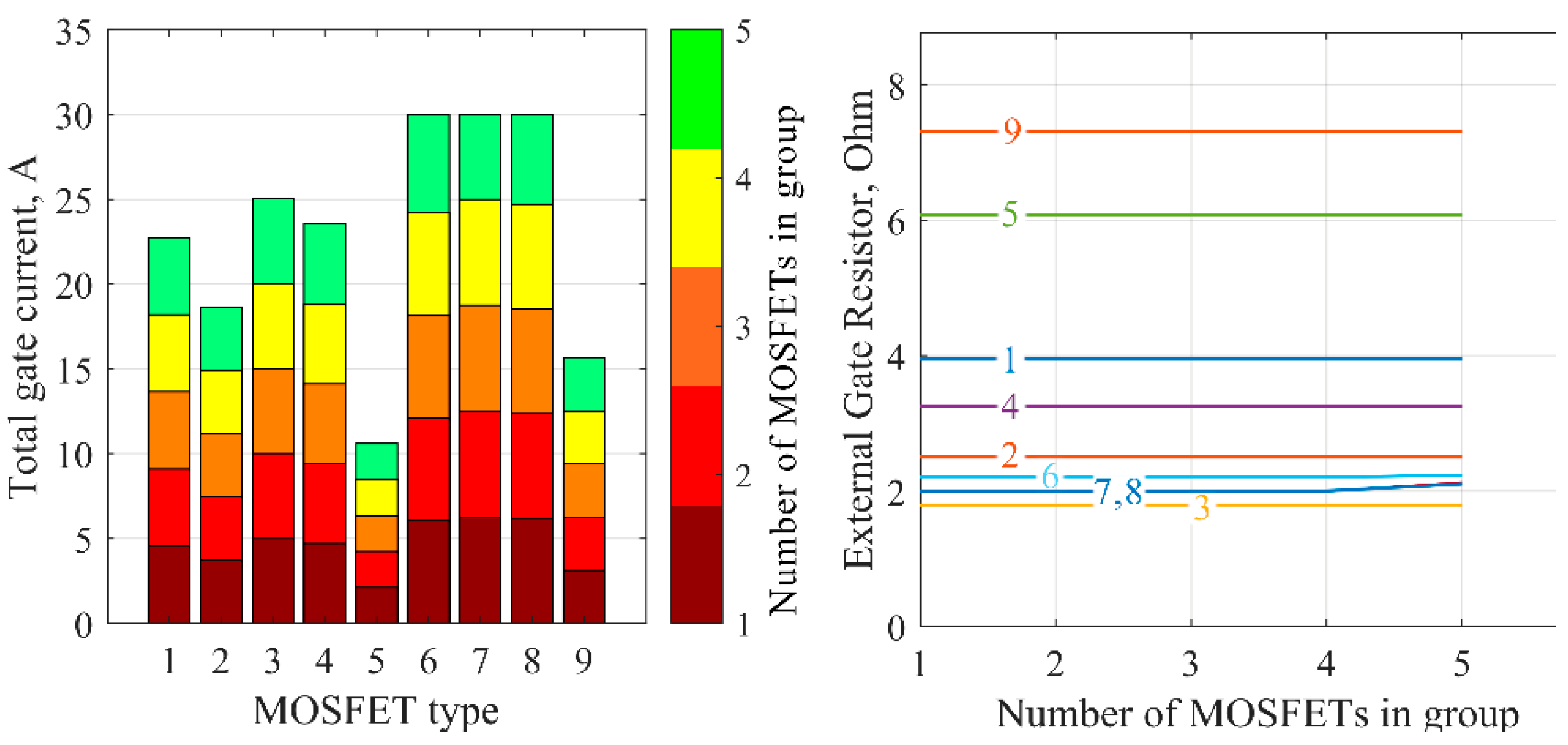
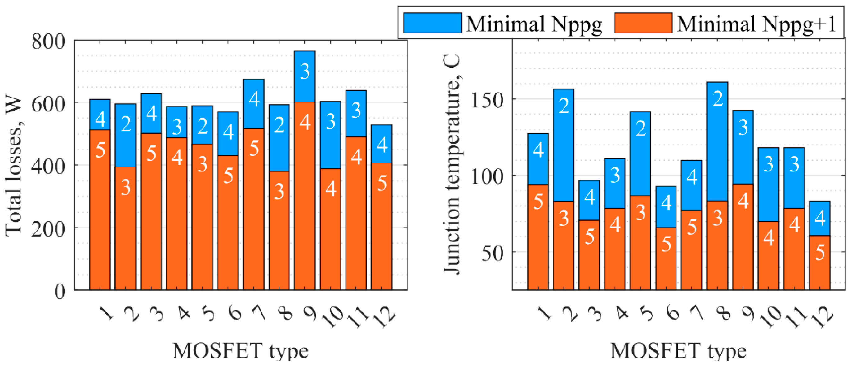
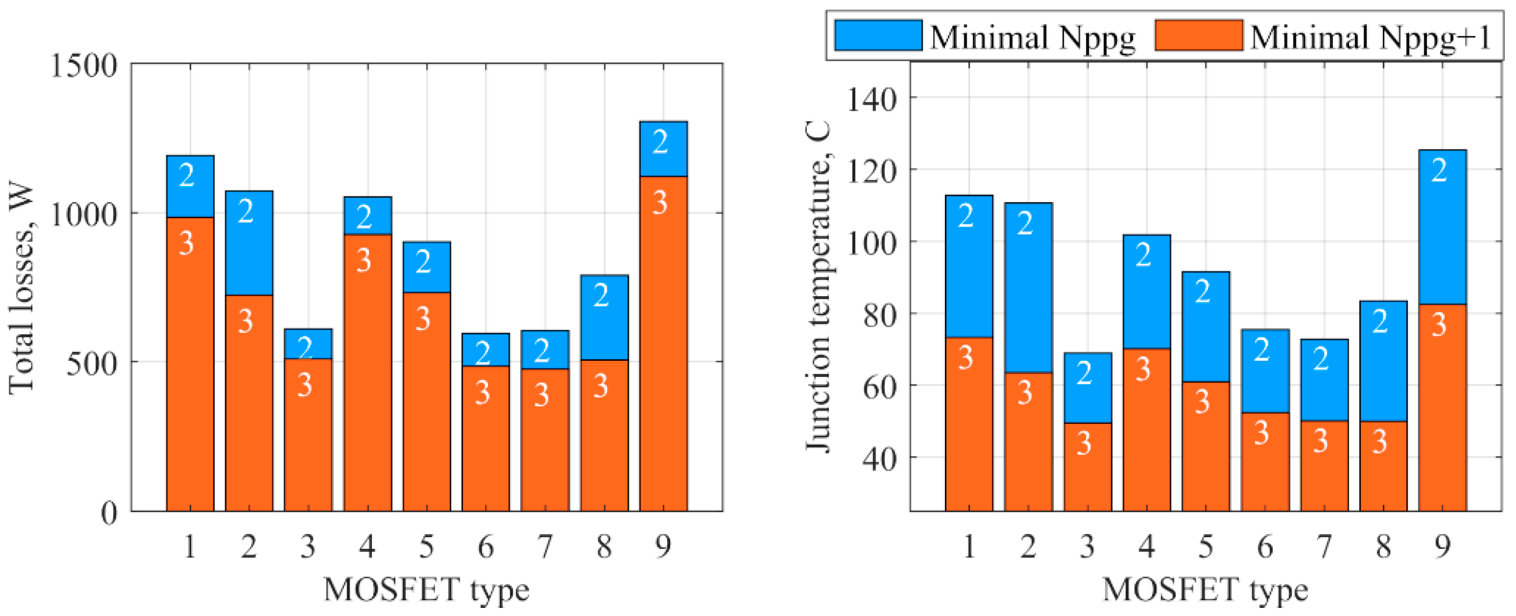
3.1. Effect of Gate Driver Current in Parallel Connection

All calculations were performed in MATLAB software package (version R2022b Update 3).
The results for the gate current analysis are presented in Figure 5 (for SMT MOSFETs), Figure 6 (for THT MOSFETs) and Figure 7 (for power modules). Different behaviors of R g   e x t could be noticed with a current limitation ( R g   e x t changed with the increase in N P P G ) and without a current limitation ( R g   e x t was constant).
The maximum number of parallel devices was set to 8 for SMT MOSFETs and 5 for THT MOSFETs.
The THT MOSFETs showed almost the same pattern with the only difference that fewer devices reached the maximum gate current threshold due to the lower number of devices per group.
The power modules showed a wide variety of results in terms of gate current, but relatively high inner and minimum external resistances limited the switching capabilities significantly, so no module could reach 30 A of gate current.

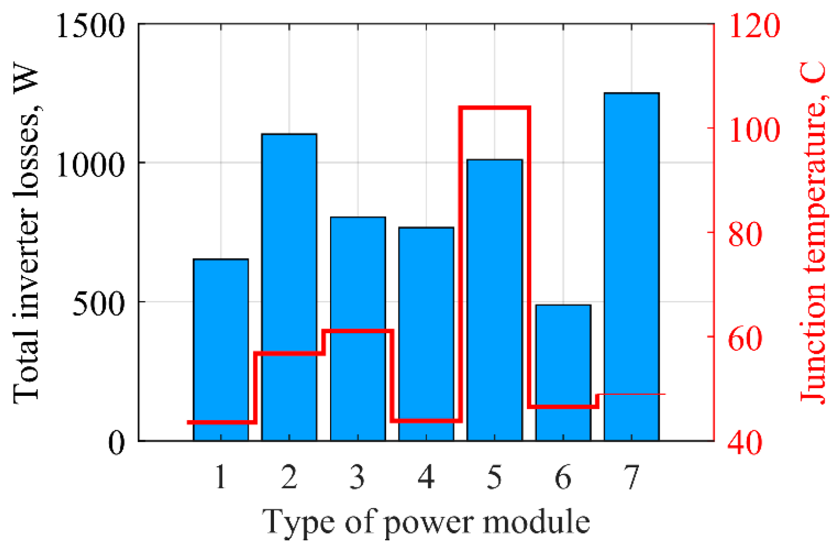
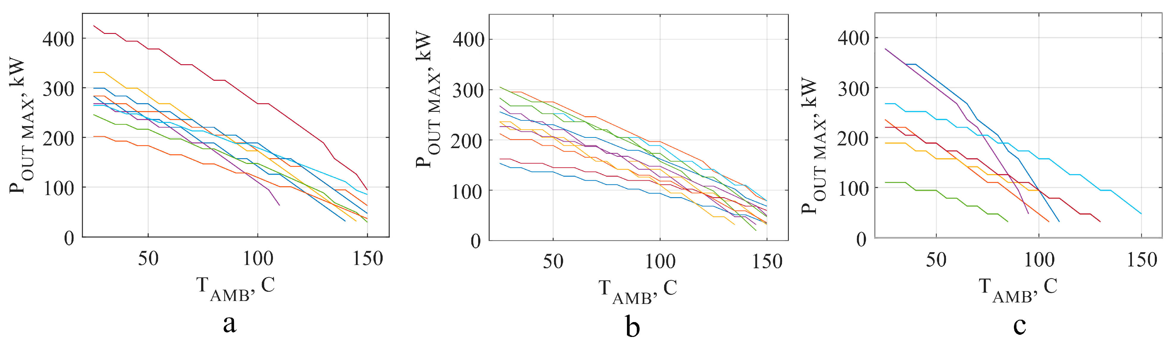
3.2. Case 1—Operation under Normal Ambient Temperature

This scenario included a detailed analysis of inverter operation under a normal ambient temperature of 25 °C. The system parameters used in the calculation are presented in Table 3; the values were chosen according to the requirements for a typical low-power IMD (for example, [26,27,28]). The discrete MOSFETs were connected in parallel and the number of devices per group was selected according to the device’s calculated maximum junction temperature.
Individual results for the different packages are presented in Figure 8, Figure 9 and Figure 10. For discrete MOSFETs, two sets of data with a different number of parallel devices ( N P P G   M I N and N P P G   M I N + 1 ) indicated the change in thermal conditions if the number of devices is increased to obtain a safety gap and reduce thermal stress. SMT devices showed the highest average junction temperature, with a significant drop (20–60 °C) in the junction temperature for the case of N P P G   M I N + 1 .
The average junction temperature for THT devices was lower by approximately 30 °C than the value for SMT packages and decreased by another 20 °C for a larger group. All devices could achieve the required performance with only two devices per group, but the total losses showed higher values than for SMT devices.
Power modules showed the same level of total losses and, in general, low values for the junction temperature (presented in Figure 10). Although compact three-phase power modules (№5) had the highest junction temperature among other modules and average total losses for a given power level, the small package gives them an obvious advantage in applications with mass or volume restrictions.
It is worth mentioning that the analysis of an inverter’s mechanical characteristics should not only consider the pure dimensions and weight of the semiconductor devices, but should also include other components of the inverter. Otherwise, the comparison demonstrates overly optimistic results (reduction by 5–10 times) for discrete components that are difficult to obtain in real applications. Some additional values can be introduced to obtain adequate figures for the characteristics of the inverter (see Table 4).
According to the calculations (see Figure 11), the inverter area and volume with their maximum numbers of MOSFETs were almost the same for both THT (package TO-247-4) and SMT devices (package TO-263-7). The different color areas for SMT and TO-247 show the number of parallel devices (from 1 to 8 for SMT, from 1 to 8 for TO-247). Different colors and corresponding numbers for modules indicate the exact type numbers.
Power modules showed significant deviations in dimensions and weight from the average level due to differences in the package design and ampacity. In fact, there was no significant difference in the inverter’s area or volume between discrete components and power modules. Nevertheless, almost all options with modules were heavier than assemblies of discrete MOSFETs; therefore, discrete components are a better choice if the weight is a target parameter of the system design.
The radar diagrams in Figure 12 compare the obtained results between packages. The values were normalized using the maximum value among all types of devices for each comparative characteristic. The color area shows the range of values for all components from that group. Furthermore, the results for three MOSFETs from each package are shown to illustrate the relationship between parameters.

3.3. Case 1—Operation under High Ambient (Coolant) Temperature Tamb = 25–150 °C

The graph of the total losses and junction temperature as functions of ambient temperature (see Figure 13) for SMT devices shows the maximum ambient temperature for each type (vertical line and the number of MOSFET types). For most types, this temperature was between 140 °C and 150 °C for the given thermal properties of the PCB and the heatsink, and only two types could work at 150 °C or higher. In the plot, P ( T a m b ), the region shaded with red color, shows the maximum amount of heat that can be transferred from the board in the case of eight parallel MOSFETs with a surface temperature of 175 °C. The total MOSFET losses must stay below the red line to keep the junction temperature within the allowed region.
THT MOSFETs showed a better performance under harsh operating conditions, as four types could work within a specified temperature range (see Figure 14).
The situation was different for power modules due to restrictions on the maximum case (baseplate) temperature. The absolute value is 125 °C for most devices, which might be a drawback for high temperature (HT) applications. The analysis results for power modules are shown in Figure 15.

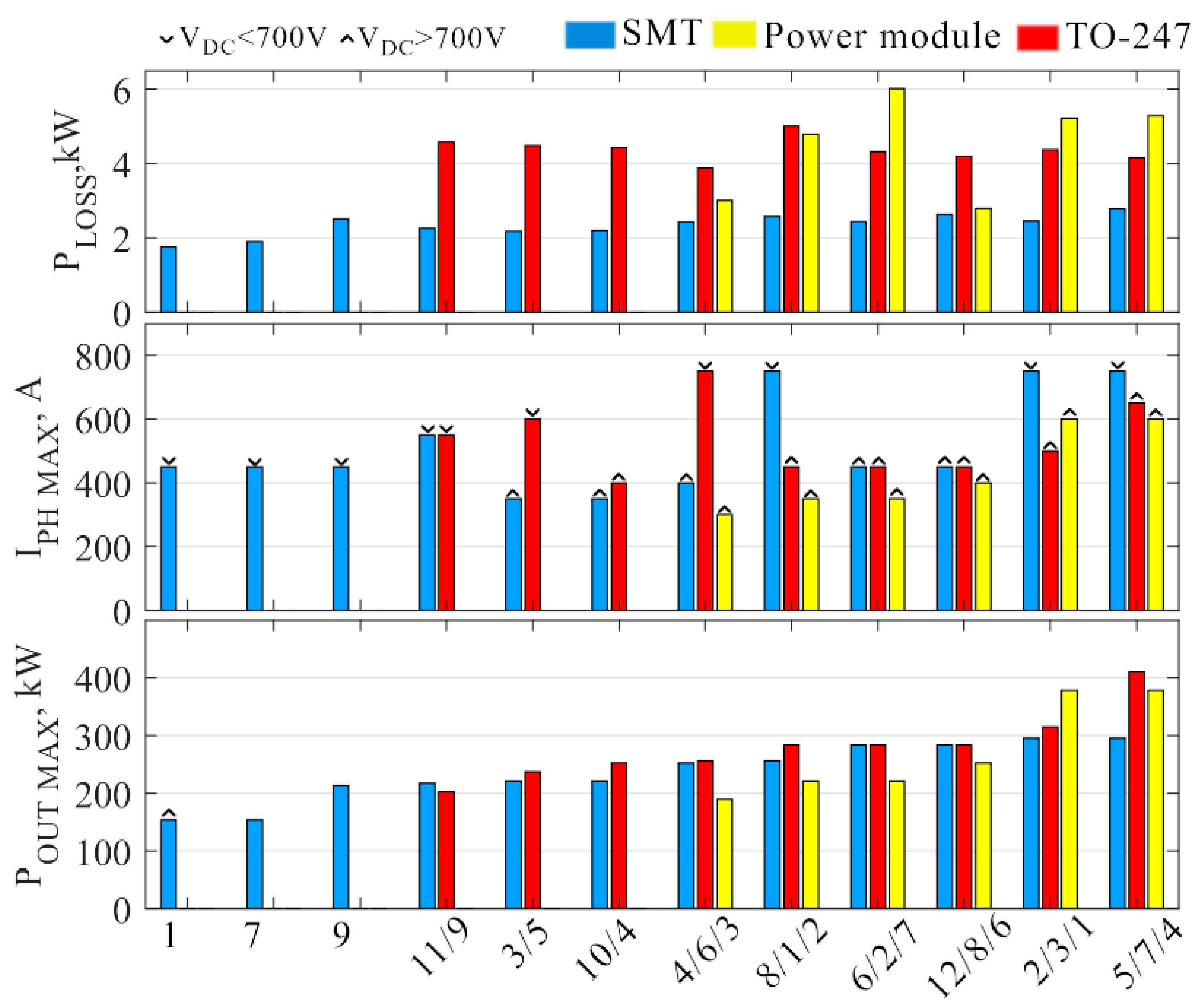
3.4. Maximum Possible Output Power and Individual DC-Link Voltage (Case 2)

All devices operated at the absolute maximum of their junction temperature T J and the number of parallel devices (for discrete MOSFETs) was set to the maximum so the highest output power could be achieved. In real applications, it is impractical to operate at the absolute maximum of junction temperature. However, this approach can still highlight general trends, reveal issues, and helps to compare the performance of different devices in various operating conditions.
It is essential to mention that the DC-link voltage V D C was different for different MOSFETs and equal to 0.7· V D C   m a x ; therefore, a higher maximum blocking voltage helped reaching top figures in output power. An indicator of the DC-link voltage V D C (high or low level) is provided in the maximum phase current plot above the MOSFETs’ bars.
The results of the performance analysis under the normal ambient temperature of all packages are presented in Figure 16 including plots for total losses, maximum phase current and maximum output power. The number of devices is mentioned on the x-axis (SMT-first, power module-last). As expected, devices with 600 V blocking voltage showed a higher maximum phase current than 1200 V devices; however, their output power was still below the results of high voltage competitors. Although new SMT packages (PowerFLAT 8 × 8 HV №1 and H−PSOF8L №7) cannot deliver high output power, they can commutate decent output phase current and, therefore, be useful in height-limited applications (package height is 0.8 mm and 2.3 mm, respectively, against 4.5 mm for TO-263-7). THT MOSFETs demonstrated a higher output power (up to 400 kW) at the expense of an increase in total losses (more than 4 kW in average). Similar to SMT MOSFETs, TO-247 devices with lower V D S   m a x reached a higher current, but the dominant role in maximum output power belonged to 1200 V MOSFETs. Due to the significant deviation in characteristics, power modules showed a wide range in both power losses and maximum output power; nevertheless, most modules could deliver 200–250 kW. The inverter’s power losses followed the distribution of output power with maximum values for power modules and THT MOSFETs. At the same time, the maximum phase current was almost the same for all packages; therefore, all packages might be used in applications with limited DC link voltage (<450 V) and a high phase current.
The mediocre performance of power modules in the analysis can be explained by the underrating of the heat sink’s efficiency (low heat transfer coefficient). The selected parameters of cooling system provided enough thermal conductivity for SMT and THT devices, as the influence of PCB or insulation layer is significant in the total thermal conductivity. By contrast, the combined thermal resistance of a power module and thermal grease is comparable with the resistance of the heat sink, limiting the potentially high performance of power modules. A higher flow rate of coolant or more sophisticated structure can increase the efficiency and, therefore, the power module’s figures (see Figure 17).
Graphs P O U T ( T a m b ) for each power device from all three package types demonstrated a derating in output power with an increase in ambient temperature (see Figure 18). SMT and THT devices experienced an almost linear reduction in output power from 200–300 kW at 25 °C to less than 100 kW at 150 °C.
Although some modules demonstrated excellent results at a normal ambient temperature, they had higher rates of power reduction due to limited T C A S E as mentioned before. Power modules without case temperature restrictions showed better results, for example, GE12047CCA3. This module, similar to discrete elements, was limited only by the junction temperature, giving more freedom for a temperature distribution between junction and case points. Moreover, it had a small negative coefficient d E S W ( d T J ) that maintained its switching losses almost at the same level within a whole range of operating temperature.

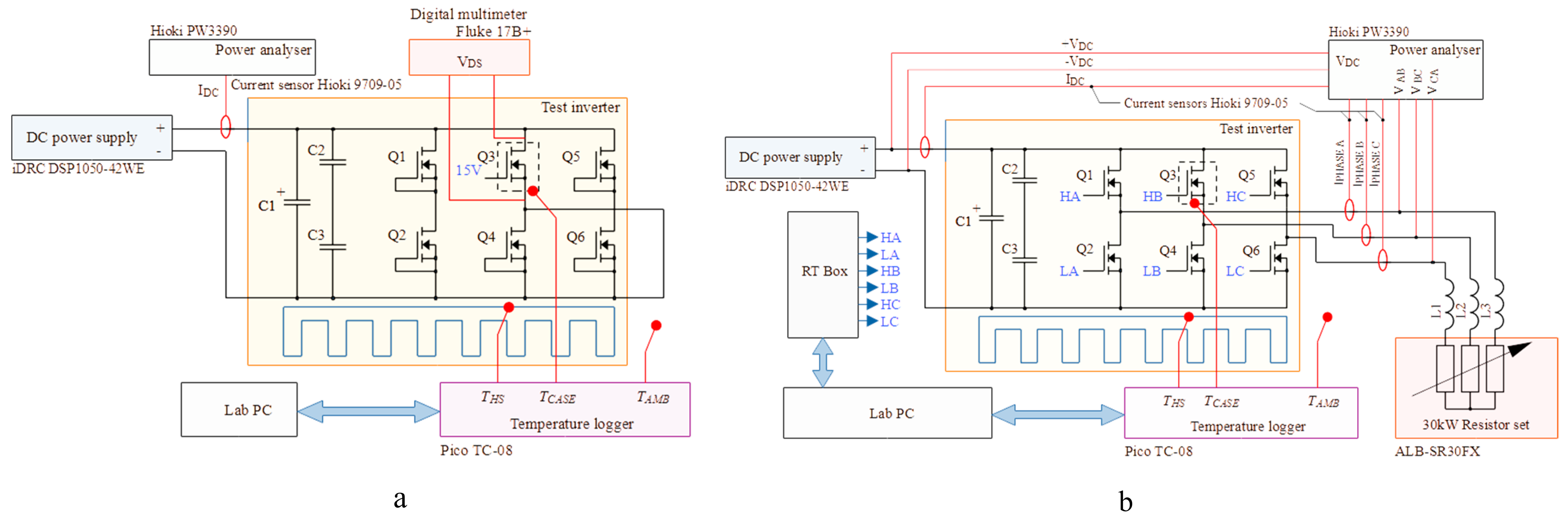
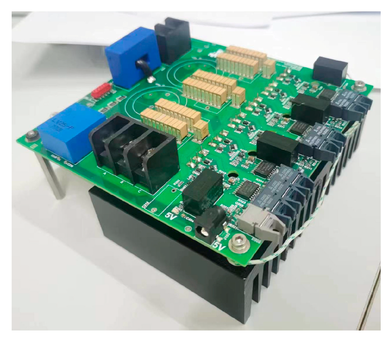
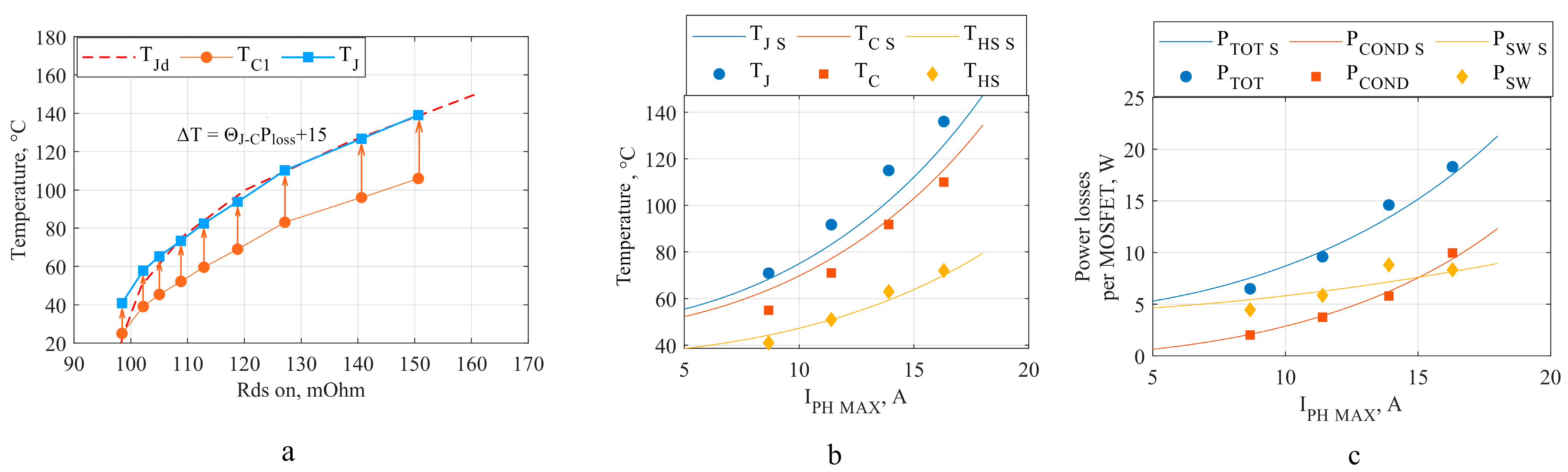
4. Experimental Validation

A three-phase two-level inverter was selected to validate the proposed thermal model of power devices’ operating conditions. The switching group of the inverter included a single SiC MOSFET C2M0080120D connected to an air-cooled heat sink. The testing conditions and system characteristics are summarized in Table 5 and some components of test inverter are mentioned in Table A4.
The goal of the procedure was to obtain experimental values of T J and P l o s s and compare them with the simulation results. The system parameters from Table 5 and MOSFET characteristics from Table A2 were used to simulate the performance of the test inverter using the proposed calculation model, and predict its power losses and the junction temperature. The flowchart of the experiment is presented in Figure 19. The first stage was required to create a valid and accurate temperature scale of the MOSFET’s junction temperature T J . The temperature sensor was located on the top surface of the MOSFET’s case; therefore, it measured temperature T C 1 close to the virtual case temperature T C .
The connection of the experimental setup for both parts of the test is presented in Figure 20. During the first part, the DC power supply worked in current control mode, and only Q3 conducted. The drain-source voltage V D S was measured with high accuracy at source and drain pins of the MOSFET were measured using a voltmeter with a large averaging period. The temperature sensors were K-type thermocouples attached to the MOSFETs and heatsink surfaces using thermal conductive material. A photo of the test inverter is demonstrated in Figure 21.
The junction temperature T J and P l o s s could be evaluated with high accuracy in this stage due to the high temperature coefficient of resistance, stable value of direct current and precise voltage measurement. In Figure 22a, a curve of the datasheet-based junction temperature T J d indicates values that were calculated according to MOSFET’s channel active resistance. The temperature difference between T J d and the case temperature should be equal to Θ J C · P l o s s ; however, the results show that the measured case temperature T C 1 had an additional constant offset of 15 °C. The proposed method (i.e., T J = T C 1 + Θ J C · P l o s s + 15   ° C ) of junction temperature evaluation fitted the curve of T J d starting from T J = 70 °C (see Figure 22). For lower junction temperatures the accuracy was not high enough due to the flat shape of R d s   o n ( T J ) .
The results of the simulation (simulated junction temperature T J S , simulated case temperature T C S , simulated heatsink temperature T H S   S , simulated total losses P T O T   S , simulated conduction losses P C O N D   S , simulated switching losses P S W   S ) are demonstrated in Figure 22b,c together with the experimentally obtained values. According to the results of the given experiment, the proposed thermal model demonstrated accuracy in power losses and junction temperature.

5. Discussion

According to the analysis results, discrete components can compete with power modules in terms of maximum output power and ability to operate under high ambient temperature. The requirements for the maximum case temperature significantly limit power modules in HT operations, and discrete components are free from such restrictions. Although a small size of packages does not lead to a guaranteed advantage in the inverter’s area or volume, the higher weight of power modules still might be considered a severe drawback in some applications.
THT devices are the best replacement for power modules in high-power inverters in most cases. In contrast to SMT MOSFETs, THT devices demonstrate low conduction losses for the 1200 V series, which is important for EV applications.
SMT devices showed a higher efficiency and compatible output current, but they were unable to reach the same power levels primarily due to the lower drain voltage. The available SMT packages suffer from the small area of thermal pads and the unavoidable presence of a PCB insulation layer. At some point, the higher number of MOSFETs in parallel cannot increase the output power because of the increased switching losses. It would be more reasonable to use these devices in applications with limited space or specific design constraints (for instance, small PCB area or the need to use PCB as a heatsink) than as a direct alternative to power modules.
In general, several devices in SMT and THT had close results, so they can be easily replaced by each other. This fact gives an obvious advantage in terms of flexibility of component selection and their availability. Manufacturers constantly modify and enhance switches by adding new features (for instance, embedded insulation for TO-247) or increasing commutating capabilities. Nevertheless, one should remember to maximize the equality in current sharing using layout symmetry and reserve a safe margin of junction temperature to compensate for a deviation in MOSFET parameters.

Author Contributions

Conceptualization, Y.M. and G.B.; methodology, Y.M.; formal analysis, Y.M.; writing—original draft preparation, Y.M.; writing—review and editing, Y.M., A.A., G.B. and M.G.; supervision, G.B. and M.G.; funding acquisition, G.B. and M.G. All authors have read and agreed to the published version of the manuscript.

Funding

This research was funded by the National Science Foundation of China (grant numbers 52377171 and 52007033).

Data Availability Statement

The raw data supporting the conclusions of this article will be made available by the authors on request.

Acknowledgments

This work is based on Chapter 3 of the PhD thesis “Considerations on the development of an integrated electric inverter for high temperature applications” of Yury Mikhaylov, submitted at the University of Nottingham Ningbo China on April 2022.

Conflicts of Interest

The authors declare no conflicts of interest. The funders had no role in the design of the study; in the collection, analyses, or interpretation of data; in the writing of the manuscript; or in the decision to publish the results.

Appendix A

Table A1. List of SMT MOSFETs.
NameYear R d s   o n , mOhm I d c   m a x , A V d c ,
V
Θ J C ,
K/W
C I S S ,
nF
T J ,
°C
A H S ,
mm2
PackageManufacturer
1SCTL90N65G2V12.202018406500.163.3817531.7PowerFLAT 8 × 8ST Microelectronics
2SCT011H75G3AG3.2022111107500.233.8317553.3H2PAK-7
3SCTH70N120G2V-78.2020219012000.323.5417553.3H2PAK-7
4AIMBG120R010M13.20238.720512000.135.717549.3PG-TO263-7-HV-ND5.8Infineon
5UJ4SC075005L8S2.20230.0051207500.18.3717576.6MO-229UnitedSiC
6G3R30MT12J11.2020308512000.33.8617544.6TO-263-7GeneSiC
7NTBL045N065SC14.202233736500.431.8717555.2H−PSOF8LOnsemi
8NVBG015N065SC12.2021121456500.34.6917552.0D2PAK−7L
9NVBG020N090SC18.2019201126500.314.4217552.0D2PAK−7L
10NTBG014N120M3P4.2022161049000.336.3117552.0D2PAK−7L
11SCT4013DW73.202313987500.435.4817565.5D2PAK-7Rohm
12SCT4018KW73.2023187512000.434.5317565.5D2PAK-7
Table A2. List of THT MOSFETs.
NameManufacturerYear R d s   o n , mOhm I d c   m a x , A V d c ,
V
C I S S ,
nF
Q g ,
µC
Θ J C ,
K/W
T J ,
°C
Package
1P3M12017K4PNJ semi6.20211715112007.290.270.19175TO-247-4
2C3M0016120KWolfspeed4.201916115120060.210.27175TO-247-4
3IMZA120R007M1HINFINEON1.2022722512009.170.220.15175PG-TO247-4-STD-T3.7
4UF3SC120009K4SUnitedSiC12.20198.612012008.50.230.15175TO 247-4L
5UJ4SC075006K4S7.20215.91207508.310.160.16175TO 247-4L
6NTH4l015N065SC1-Donsemi4.2021121426504.790.280.3175TO 247-4L
7G3R20MT12KGeneSiC1.20231215512009.340.280.26175TO 247-4
8NTH4L014N120M3Ponsemi1.20231412712006.230.330.17175TO 247-4L
9MSC015SMA070B4Microsemi 151407004.50.220.22175TO 247-4L
*C2M0080120DWolfspeed2013803612001.130.0710.6150TO 247
* only for experimental validation.
Table A3. List of power modules.
NameYear R d s   o n , mOhm I d c   m a x , A V d c ,
V
C I S S ,
nF
Q g ,
µC
Θ J C ,
K/W
T J
°C
Length, mmWidth, mmHeight, mmWeight, g
1CAB760M12HM32.20221.331015120079.42.720.0681751106512.2180
2CAB530M12BM33.20212.67719120039.61.360.065175103.560.430300
3CAB450M12XM36.20192.6450120038.01.330.11175805315.75175
4MSCSM120AM02CT6LIAG1.20202.1947120036.22.780.041751086216320
5MSCSM120TAM11CTPAG 11.20208.4251120090.690.1441751086211.5250
6GE12047CCA35.20213.1475120029.31.250.117589.351.214.8120
7FS03MR12A6MA1B 1,24.20212.75400120042.61.320.1151501549519720
1: 3-phase module, 2: designed for direct cooling.
Table A4. Components of the test inverter.
Component FunctionComponent TypeNotes
Input capacitorMAL205737101E3 (100 µF 450 V), 2 in parallel
B58035U5106M001 (10 µF 500 V), 3 in parallel
C1
C2, C3
Gate drivers1ED3320MC12N
Power switchesC2M0080120DQ1–Q6
DC-link snubber capacitorB32714H1205K000 (2 µF 1100 V) and
B58035U9504M (500n 900 V) in parallel

References

  1. Wheeler, P.; Bozhko, S. The More Electric Aircraft: Technology and challenges. IEEE Electrif. Mag. 2014, 2, 6–12. [Google Scholar] [CrossRef]
  2. Calzo, G.; Vakil, G.; Mecrow, B.C.; Lambert, S.; Cox, T.; Gerada, C.; Johnson, M.; Abebe, R. Integrated Motor Drives: State of the Art and Future Trends. IET Electr. Power Appl. 2016, 10, 757–771. [Google Scholar] [CrossRef]
  3. Renken, F. High temperature electronics for future hybrid drive systems. In Proceedings of the 2009 13th European Conference on Power Electronics and Applications, Barcelona, Spain, 8–10 September 2009; pp. 1–7. [Google Scholar]
  4. Lee, W.; Li, S.; Han, D.; Sarlioglu, B.; Minav, T.A.; Pietola, M. Achieving high-performance electrified actuation system with integrated motor drive and wide bandgap power electronics. In Proceedings of the 2017 19th European Conference on Power Electronics and Applications (EPE’17 ECCE Europe), Warsaw, Poland, 11–14 September 2017; pp. P.1–P.10. [Google Scholar]
  5. Chen, C.; Chen, Y.; Li, Y.; Huang, Z.; Liu, T.; Kang, Y. An SiC-Based Half-Bridge Module With an Improved Hybrid Packaging Method for High Power Density Applications. IEEE Trans. Ind. Electron. 2017, 64, 8980–8991. [Google Scholar] [CrossRef]
  6. Wang, R.; Boroyevich, D.; Ning, P.; Wang, Z.; Wang, F.; Mattavelli, P.; Ngo, K.D.T.; Rajashekara, K. A High-Temperature SiC Three-Phase AC–DC Converter Design for > 100/spl deg/C Ambient Temperature. IEEE Trans. Power Electron. 2013, 28, 555–572. [Google Scholar] [CrossRef]
  7. Ning, P.; Zhang, D.; Lai, R.; Jiang, D.; Wang, F.; Boroyevich, D.; Burgos, R.; Karimi, K.; Immanuel, V.D.; Solodovnik, E.V. High-Temperature Hardware: Development of a 10-kW High-Temperature, High-Power-Density Three-Phase ac-dc-ac SiC Converter. IEEE Ind. Electron. Mag. 2013, 7, 6–17. [Google Scholar] [CrossRef]
  8. Olejniczak, K.; Flint, T.; Simco, D.; Storkov, S.; McGee, B.; Shaw, R.; Passmore, B.; George, K.; Curbow, A.; McNutt, T. A compact 110 kVA, 140 °C ambient, 105 °C liquid cooled, all-SiC inverter for electric vehicle traction drives. In Proceedings of the 2017 IEEE Applied Power Electronics Conference and Exposition (APEC), Tampa, FL, USA, 26–30 March 2017; pp. 735–742. [Google Scholar]
  9. Zhang, C.; Srdic, S.; Lukic, S.; Sun, K.; Wang, J.; Burgos, R. A SiC-Based Liquid-Cooled Electric Vehicle Traction Inverter Operating at High Ambient Temperature. CPSS Trans. Power Electron. Appl. 2022, 7, 160–175. [Google Scholar] [CrossRef]
  10. Liu, X.; Wei, M.; Qiu, M.; Hobbs, K.; Yang, S.; Dahneem, A.; Cao, D. FPGA-Based Forced Air-Cooled SiC High-Power-Density Inverter for Electrical Aircraft Applications. In Proceedings of the 2023 IEEE Applied Power Electronics Conference and Exposition (APEC), Orlando, FL, USA, 19–23 March 2023; pp. 3169–3173. [Google Scholar]
  11. Stella, F.; Vico, E.; Cittanti, D.; Liu, C.; Shen, J.; Bojoi, R. Design and Testing of an Automotive Compliant 800V 550 kVA SiC Traction Inverter with Full-Ceramic DC-Link and EMI Filter. In Proceedings of the 2022 IEEE Energy Conversion Congress and Exposition (ECCE), Detroit, MI, USA, 9–13 October 2022; pp. 1–8. [Google Scholar]
  12. Vollmar, N.; Woehrle, D.; Armbruster, C.; Schoener, C. Design of a Fast Switching 200 kVA SiC Drive Inverter for Aviation Application. In Proceedings of the PCIM Europe 2023; International Exhibition and Conference for Power Electronics, Intelligent Motion, Renewable Energy and Energy Management, Nuremberg, Germany, 9–11 May 2023; pp. 1–8. [Google Scholar]
  13. Mikhaylov, Y. Considerations on the Development of an Integrated Electric Inverter for High Temperature Applications. Ph.D. Thesis, University of Nottingham Ningbo China, Ningbo, China, 2023. [Google Scholar]
  14. FF2MR12KM1HP. Available online: https://www.infineon.com/cms/en/product/power/mosfet/silicon-carbide/modules/ff2mr12km1hp/ (accessed on 10 November 2023).
  15. Wolfspeed HM3 High-Performance Half-Bridge Modules. Available online: https://www.mouser.com/new/wolfspeed/wolfspeed-hm3-half-bridge-modules/ (accessed on 10 November 2023).
  16. MSCSM120AM02CT6LIAG-Module. Available online: https://www.microchip.com/en-us/product/mscsm120am02ct6liag-module (accessed on 10 November 2023).
  17. Wang, Z.; Luo, B.; Zhan, J.; Zhou, H.; Zhan, X.; Li, T.; Ye, C.; Tian, J. A 200 kW high-efficiency and high-power density xEV motor controller based on discrete SiC MOSFET devices. Int. J. Circuit Theory Appl. 2022, 50, 3053–3070. [Google Scholar] [CrossRef]
  18. Chen, Z.; Rizi, H.S.; Chen, C.; Liu, P.; Yu, R.; Huang, A.Q. An 800V/300 kW, 44 kW/L Air-Cooled SiC Power Electronics Building Block (PEBB). In Proceedings of the IECON 2021—47th Annual Conference of the IEEE Industrial Electronics Society, Toronto, ON, Canada, 13–16 October 2021; pp. 1–6. [Google Scholar]
  19. Taha, W.; Juarez-Leon, F.; Hefny, M.; Jinesh, A.; Poulton, M.; Bilgin, B.; Emadi, A. Holistic Design and Development of a 100 kW SiC-Based Six-Phase Traction Inverter for an Electric Vehicle Application. IEEE Trans. Transp. Electrif. 2023. [Google Scholar] [CrossRef]
  20. Costa, P.; Pinto, S.; Silva, J.F. A Novel Analytical Formulation of SiC-MOSFET Losses to Size High-Efficiency Three-Phase Inverters. Energies 2023, 16, 818. [Google Scholar] [CrossRef]
  21. Yu, S.; Wang, J.; Zhang, X.; Liu, Y.; Jiang, N.; Wang, W. The Potential Impact of Using Traction Inverters with SiC MOSFETs for Electric Buses. IEEE Access 2021, 9, 51561–51572. [Google Scholar] [CrossRef]
  22. Cittanti, D.; Guacci, M.; Mirić, S.; Bojoi, R.; Kolar, J.W. Comparative Evaluation of 800V DC-Link Three-Phase Two/Three-Level SiC Inverter Concepts for Next-Generation Variable Speed Drives. In Proceedings of the 2020 23rd International Conference on Electrical Machines and Systems (ICEMS), Hamamatsu, Japan, 24–27 November 2020; pp. 1699–1704. [Google Scholar]
  23. Yapa, R.; Forsyth, A.J.; Todd, R. Analysis of SiC technology in two-level and three-level converters for aerospace applications. In Proceedings of the 7th IET International Conference on Power Electronics, Machines and Drives (PEMD 2014), Manchester, UK, 8–10 April 2014; pp. 1–6. [Google Scholar]
  24. Merkert, A.; Krone, T.; Mertens, A. Characterization and Scalable Modeling of Power Semiconductors for Optimized Design of Traction Inverters with Si- and SiC-Devices. IEEE Trans. Power Electron. 2014, 29, 2238–2245. [Google Scholar] [CrossRef]
  25. Oswald, N.; Anthony, P.; McNeill, N.; Stark, B.H. An Experimental Investigation of the Tradeoff between Switching Losses and EMI Generation with Hard-Switched All-Si, Si-SiC, and All-SiC Device Combinations. IEEE Trans. Power Electron. 2014, 29, 2393–2407. [Google Scholar] [CrossRef]
  26. Nikouie, M.; Zhang, H.; Wallmark, O.; Nee, H. A highly integrated electric drive system for tomorrow’s EVs and HEVs. In Proceedings of the 2017 IEEE Southern Power Electronics Conference (SPEC), Manchester, UK, 4–7 December 2017; pp. 1–5. [Google Scholar]
  27. Deng, X.; Lambert, S.; Mecrow, B.; Mohamed, M.A.S. Design Consideration of a High-Speed Integrated Permanent Magnet Machine and its Drive System. In Proceedings of the 2018 XIII International Conference on Electrical Machines (ICEM), Alexandroupoli, Greece, 3–6 September 2018; pp. 1465–1470. [Google Scholar]
  28. Lee, W.; Li, S.; Han, D.; Sarlioglu, B.; Minav, T.A.; Pietola, M. A Review of Integrated Motor Drive and Wide-Bandgap Power Electronics for High-Performance Electro-Hydrostatic Actuators. IEEE Trans. Transp. Electrif. 2018, 4, 684–693. [Google Scholar] [CrossRef]
Figure 1. Different packages of SiC MOSFETs [13].
Electronics 13 00355 g001
Figure 2. Power modules with different terminal locations: (a)—Infineon CoolSiC module [14]; (b)—Wolfspeed HM3 module [15]; (c)—microchip power module [16].
Electronics 13 00355 g002
Figure 3. Layout for SMT (TO-263-7) and THT (TO-247) components.
Electronics 13 00355 g003
Figure 4. Flowchart for the calculation of junction temperature.
Electronics 13 00355 g004
Figure 5. Total gate current and external gate resistance of SMT MOSFETs.
Electronics 13 00355 g005
Figure 6. Total gate current and external gate resistance of THT MOSFETs.
Electronics 13 00355 g006
Figure 7. Total gate current and external gate resistance of power modules.
Electronics 13 00355 g007
Figure 8. Total losses and junction temperature of SMT MOSFETs in Scenario 1 ( T a m b = 25 °C).
Electronics 13 00355 g008
Figure 9. Total losses and junction temperature of THT MOSFETs in Scenario 1 ( T a m b = 25 °C).
Electronics 13 00355 g009
Figure 10. Total losses and junction temperature of power modules in Scenario 1 ( T a m b = 25 °C).
Electronics 13 00355 g010
Figure 11. Results of dimension analysis (additional values are included).
Electronics 13 00355 g011
Figure 12. Normalized analysis results for the (minimum + 1) number of parallel devices T a m b = 25 °C ((a)—THT, (b)—SMT, (c)—power modules).
Electronics 13 00355 g012
Figure 13. Total losses and junction temperature of SMT MOSFETs in Scenario 1 ( M a x   P L O S S represents the maximum heat that can be removed by an area of eight packages).
Electronics 13 00355 g013
Figure 14. Total losses and junction temperature of THT MOSFETs in Scenario 1 ( M a x   P L O S S represents the maximum heat that can be removed by the total heatsink area).
Electronics 13 00355 g014
Figure 15. Total losses and junction temperature of power modules in Scenario 1 ( T a m b = 25–150 °C).
Electronics 13 00355 g015
Figure 16. Simulation results of MOSFETs with maximum output power T a m b = 25 °C.
Electronics 13 00355 g016
Figure 17. Ranges of maximum output power (all devices are included) for different packages under normal ambient temperature T a m b = 25 °C and various efficiency of the cooling system.
Electronics 13 00355 g017
Figure 18. Maximum output power for THT (a), SMT (b) and power modules (c) devices within the range T a m b = 25–150 °C.
Electronics 13 00355 g018
Figure 19. Algorithm of the experiment to obtain T J and P l o s s .
Electronics 13 00355 g019
Figure 20. Test setup for Rds measurements (a) and 3-phase inverter operation (b).
Electronics 13 00355 g020
Figure 21. Test inverter for the experiment setup.
Electronics 13 00355 g021
Figure 22. Experimental results: (a) calibration of T C measurement at 1st stage; (b) comparison between predicted and measured temperatures (junction, case and heatsink); (c) comparison between predicted and measured power losses for a MOSFET (total, conduction and switching).
Electronics 13 00355 g022
Table 1. Default values of coefficients for losses calculation.
Coefficient NameEquation’s Parameters’ Default ValuesCoefficient Default Value
K R G Not applicable R g   e x t + R g   i n n e r R g   e x t   r a t e d + R g   i n n e r
K T J A T J = 0 , B T J = E S W   t o t   r a t e d 1
K V D C A V D C = 1.4 V D C V D C r a t e d 1.4
  K I D S A I D S = C I D S = 0 , B I D S = E S W   t o t   r a t e d I D S   m a x   r a t e d I D S   m a x I D S   m a x   r a t e d
K R T J R n d s   o n   T J   H T = 1 0
K R I A R I = 0 , B R I = R d s   o n 25 1
Table 2. Thermal resistances of the utilized calculation model.
Input ParameterDevice TypeValueCalculated ParameterDevice TypeValue
Prepreg thickness, mmSMT0.1 Junction ambient   thermal   resistance   θ s i n g l e (per MOSFET), K/WSMT2.66–4
Prepreg thermal conductivity, W/m·K1
Top copper layer thickness, mm0.07
Insulation (mica + grease) thermal resistance per area, K/cm2·KTHT0.65 Junction ambient   thermal   resistance   θ s i n g l e (per MOSFET), K/WTHT0.88–1.05
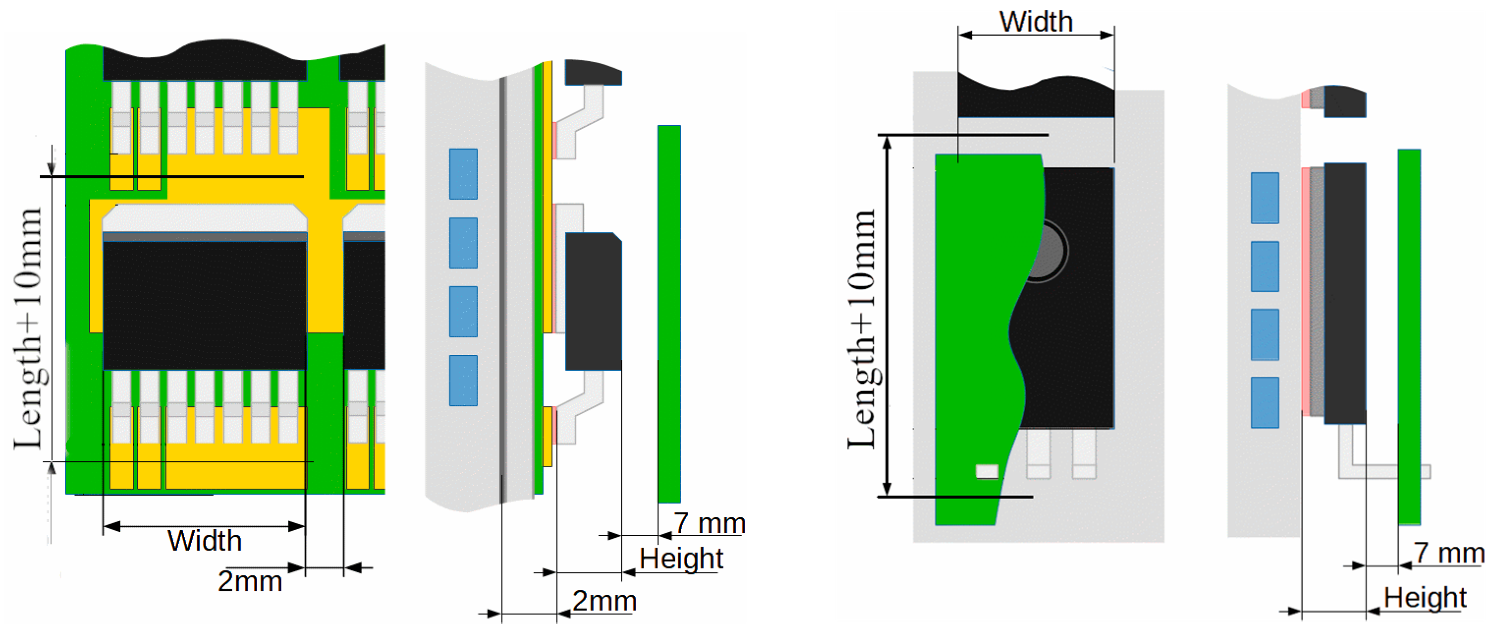
Heat sink area per a MOSFET (for SMT and THT), mm2SMT/THT(L + 10)·(W + 2) Junction ambient   thermal   resistance   θ s i n g l e (per MOSFET), K/Wpower modules0.148−0.54
Grease thermal conductivity, W/m·KSMT/THT/Modules0.73
Heatsink heat transfer coefficient, W/cm2·K0.5
L, W—length and width of MOSFET’s case.
Table 3. IMD parameters for comparative analysis.
ParameterValue
Peak   phase   current   I P H   m a x , A200
DC   voltage   V D C , V400
Switching   frequency   F s w , kHz50
Coolant   temperature   T C O O L A N T , °C25
HTC   of   the   cold   plate   h c p , W/cm2·K0.5
Table 4. Additional values for dimensional analysis of the inverter.
ParameterAreaWeightVolume
Additional values1.5 cm *1.5 kg **1.5 L **
*—to each side of a switching group (for screws, tolerance, etc.). **—that includes other components, a case and a heatsink, total power density is approximately 30 kW/L(or 30 kW/kg).
Table 5. Characteristics of the testing inverter.
V D C , V F s w , kHz F f u n d , kHzLoad (per Phase) Θ h s a m b ,   K W Θ c h s ,   K W
3505010.5 mH, 8.6–16.8 Ohm0.422.9–4
Disclaimer/Publisher’s Note: The statements, opinions and data contained in all publications are solely those of the individual author(s) and contributor(s) and not of MDPI and/or the editor(s). MDPI and/or the editor(s) disclaim responsibility for any injury to people or property resulting from any ideas, methods, instructions or products referred to in the content.

