1. Introduction
For companies producing electronic modules, one of the most important processes, apart from the production process, is the repair process [
1,
2]. Both processes are subject to specific requirements and quality standards [
3]. By establishing an appropriate repair process, it is possible to recover some non-compliant material and thus reduce material loss (TML) [
3,
4,
5]. The impacts of maintaining production processes of sufficient quality, controlling for non-compliant material, and implementing a repair process are described in various articles [
1,
6,
7,
8,
9].
The goal is to create conditions for separating non-compliant material from the production process, assessing the level of non-compliance and reparability, and as a result, determining the location in the production area that is the source of the problem in order to eliminate it.
When producing electronic modules, some of the resulting material will comply with the requirements and standards, and some of it will be non-compliant. It is therefore important for an overall production process to include a sub-process for identifying and separating compliant and non-compliant materials, assessing the levels of non-compliance and reparability of non-compliant material, and as a result, determining the source of the problem in order to eliminate it. In this way, identifying and analyzing damaged modules can improve the production process by eliminating sources of non-compliance (Failure Analysis) [
10,
11,
12].
An increase in the quality of the production process is guaranteed to offset the initially large cost of implementing a repair process. This cost may be quite high, as it includes the expenses of developing and refining the repair process, hiring technicians and training them, acquiring repair stations (including analysis and measurement devices), and acquiring storage space for defective modules. However, once implemented, investments in the repair process yield a positive return on investment [
4]. Thus, it becomes cheaper to invest in a repair process rather than to omit it [
13,
14].
The ideal production process does not require corrective actions as the manufactured products will always meet the design specifications, client expectations, and quality and safety standards. Unfortunately, such a process does not exist, and there is always a risk of a defective product [
7,
15,
16,
17,
18]. Therefore, TML reduction is one of the key indicators measured. It is worth incurring the cost of developing a good repair process and including a Repair Department in the company’s organizational structure, because it will result in TML reduction and therefore a positive return on investment.
It is also important to note that, to date, there is no single standard tool on the market that meets all the expectations and functions required to control the performance of a production line and simultaneously to support the repair process [
16,
19,
20]. The costs of development efforts required to create such a tool are typically too high for companies to undertake. Instead, companies typically make in-house efforts that either copy existing functionality from separate, individual tools into a monolithic platform, or create a single interface that links the tools together.
The aim of our article is to present a new system supporting the diagnostics of electronic modules. The system inspectAR elaborated by us is based on the augmented reality solution. It makes it easy to find any component in the tested module and obtain the indispensable information about such a component in a fast way. The use of the proposed system makes it possible to speed up the repair process and to lower its costs. The sections describe: the repair process; the origin and functions of the inspectAR tool from Cadence, a realistic example of the debugging and repair processes in an industrial production setting; a discussion of how inspectAR’s use aids these processes, and areas where inspectAR could be enhanced.
2. Steps of the Repair Process
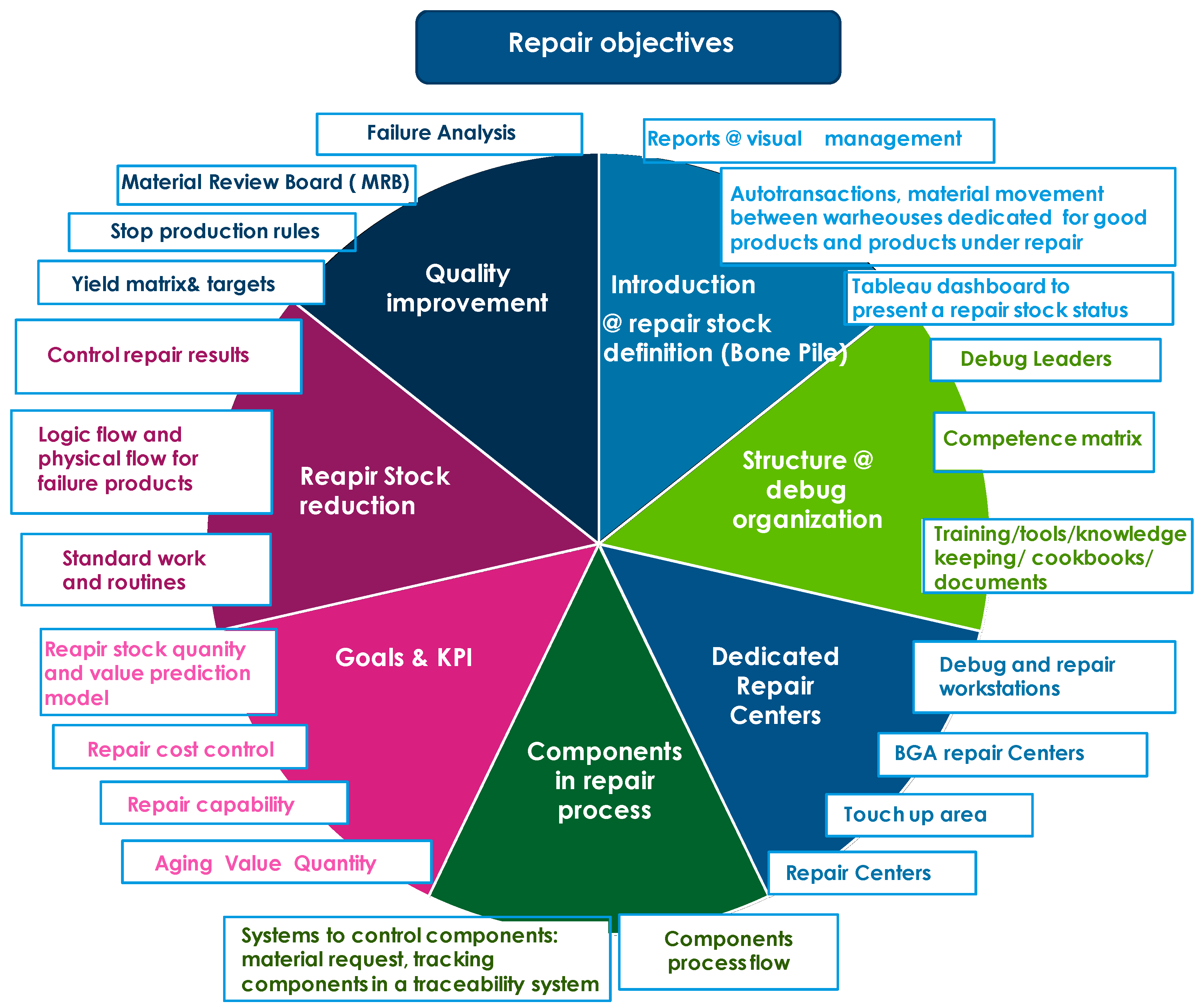
The repair process has many facets, and touches many areas of the company and its production process. To be effective, the repair process must be comprehensive and extend beyond the repair actions employed by specialists during debugging and reworking. A wide range of methods, reports, and actions (
Figure 1) can be implemented to provide full control over repair stocks and to efficiently reduce TML. Such a comprehensive and far-reaching system is typically put in place as part of a strategic decision by management to reduce TML.
A proper repair process not only involves service activities. Therefore,
Figure 1 presents a whole range of different methods, reports, and actions to fully control repair stocks and the efficiency of their reduction.
Starting from the definition of the risk associated with the material collected for repairs, through an appropriate organizational structure, one can move on to specifics related to the equipment of repair stations and the construction of repair centers [
6]. It is necessary to equip repair stations with specialized equipment for performing tests on, debugging, and reworking electronic modules. It is also important to employ warehouse services to support the repair process by delivering modules and components to the appropriate stations. The tracking of and control over the flow of materials is possible with a traceability system. In this regard, warehouse services should also be provided to deliver components for repairs. The course of the repair activities applied to a selected example is described later in this paper, in
Section 4. Another description of such a process can be found in [
1].
The analysis, debug, and repair processes for electronic modules incur additional costs for the company. Hence, goals related to the effectiveness of the repair team’s work are set [
6]. The risk of material loss is determined by measuring the parameters of the repair, stock such as the age, quantity, and value of all products waiting for repair. These data can then be used to estimate costs and effectively manage the entire service in order to minimize cost and material loss.
Figure 2 illustrates the logistics of the defective PCBAs.
As is shown, the damaged PCBAs are collected in the defective PCBs warehouse. These PCBs are tested in order to debug their faults. Next, the repair process starts. In this process touch-up area, components and tools are indispensable. In the repair system, the reflow process is undertaken in the repair station. Next, the quality of the repaired PCBAs is tested. If the result of this test is positive, the repaired PCBs go to the repaired PCBs warehouse, and next to the final product warehouse.
After each repair, the material from the repair area must be returned to either production or storage. Again, this flow of material is tracked and controlled by the traceability system, and is supported by warehouse services. Control over the flow of material is possible thanks to the system (traceability system) controlling the status of the product at each stage.
The last stage of the repair process is incorporating feedback into the production process. This involves operational activities carried out with engineering support to use information gathered from the repair process to remedy and improve production quality. The entire process is supervised by a team of quality engineers who set priorities and monitor quality indicators of the production process, such as yield [
1,
6].
As part of the repair process, a number of tools are used to determine the status of products in the repair area, to analyze their defects, and to control the components needed for their repair. The main, most important, and most necessary systems in the production process are the following:
Traceability system—Controls the product flow, tracks the status of all manufacturing and assembly steps, and collects data to provide a full history of the product and its quality metrics. This system uses a database to collect and store knowledge about all product manufacturing processes and their results;
Test diagnostic system—Supports debug and analysis activities of faulty electronic devices. It connects the traceability system with the other databases to provide documents such as schematics, functional descriptions, repair manuals, repair statistics, and historical data of prior effective repair actions for specific failure types;
PCBA viewer—A tool dedicated to viewing PCBAs and their signals and components. It facilitates cross probing between the physical PCBA and its digital twin. It also provides access to information and documentation related to the design. The inspectAR application is an example of such a viewer;
Material replenishment system—Tools dedicated to component ordering and delivery. This system is used for material replenishment during production and repair.
For the most part, the above systems and applications stand alone and require significant manual involvement to be useful in other production operations. Each different platform requires additional specialized training for production staff and engineers. This incurs additional costs, which is why many companies try to find or create tools that contain all necessary functionality within a single application. Such solutions may be achieved through outsourcing, using internal resources, or some combination of the two.
3. Origins of inspectAR
The application inspectAR began as a mechanical XY frame (
Figure 3), similar to an automated optical inspection machine, acting as a smart microscope with augmented reality (AR) embedded information [
21]. This configuration posed a high barrier to entry, so development efforts shifted towards a mobile phone application. Future product iterations found equilibrium in a mostly desktop-based application combined with a fixed mounted external camera.
The first commercial version of inspectAR was released in August 2019. Extensive market research amongst PCB designers was an important part of the early definitions of inspectAR’s customer archetype. Market research was conducted through a pilot program of PCB designers from 2020 into early 2021. During this pilot program, a use model was constructed whereby PCB designers and other engineering professionals could plan, record, and track work completed on a PCB through the augmented reality technology that the earlier versions of inspectAR had pioneered.
In August 2020, inspectAR was acquired by Cadence. The acquisition greatly increased inspectAR’s EDA data processing capabilities by enabling the development team to pull from Cadence’s decades of experience developing PCB design technologies (such as Allegro and OrCAD).
The inspectAR app works by consuming intelligent manufacturing outputs (e.g., Cadence Allegro design files) and then overlaying design information into the user’s viewport of choice. As an intelligent workbench tool, inspectAR enables activities like rapid datasheet lookup supplied by Unified Search, and integrates with Allegro to close the design loop via procedural work orders [
22].
Given the capabilities described in this article, inspectAR proves to be an ideal solution, as its augmented reality technology resolves the location of PCB metadata in each frame of the video image. In this way, the solution goes beyond the standard requirements to provide a platform that can meet a wide range of quality needs for the foreseeable future.
5. InspectAR
When it comes to debugging and repairing, using multiple, different tools wastes time getting each setup and navigating different user interfaces. Therefore, the best tools are those that can integrate different solutions and options into a single application. One benefit of such an integrated tool is the time saved by not switching between different applications.
As a platform that can integrate with other solutions, inspectAR strives to enable diagnostic technicians to use augmented reality tools to make their daily troubleshooting and repair activities more efficient by:
Reducing fault analysis time;
Improving the efficiency of electronic module diagnostics;
Improving the production of repair manuals;
Reducing Total Material Waste (TML);
Increasing the efficiency of the repair team.
For this reason, the development efforts of inspectAR are focused on use models set within the PCB production environment. The production environment can be challenging, as there are uptime and availability requirements at a large-scale. Production IT requirements may also dictate that software must run on a local server. Additionally, there may be significant variance in the size and shape of produced electronic modules. The development of inspectAR has addressed, and continues to refine, use models within these constraints.
The general steps in the repair and debugging process follow the sequence shown in
Table 1.
In this general workflow, as shown in
Table 1, many additional documents, schematics, repair histories and diagnostic tools are used from step 4 onwards to locate and correct a fault. The search for components and signals associated with a problem in a PCBA circuit begins with a review of the component connection documentation on the schematic and on the functional description. The block diagram serves as the bridge between these two documents.
To illustrate the debug and repair process, an example PCBA (printed circuit board assembly) is presented (
Figure 6). The example PCBA (printed circuit board assembly) presented here consists of several layers. Its controller has universal inputs and outputs (I/O) and a Trusted Platform Module (TPM) connection transcription module to increase the security of recorded and stored data.
Many different problems can occur in the presented circuit shown in
Figure 6, the solutions for which can be sought by understanding the logic and functionality of its individual blocks. Most often they can be found in the dedicated documentation mentioned above, which contain a description of the basic assumptions of the module.
The operation of the module is checked through prepared software procedures as part of a functional test verifying that the device operates in accordance with the assumptions described by the customer. They appear in the “test plan”, a designed test sequence specific to the device. The preparation of the test and the signal transmission interface standard are separate topics, and are defined by the design and functional requirements of each individual electronic module.
In the considered electronic module, one of the basic functional tests verifying its correct operation is the condition that the device must load and execute the test firmware to enter a “netboot” mode. The test is timed, and to pass, the device must respond that the firmware has been started within a limited period (20 s in this case).
The above test may be failed for various reasons. One problem that arises is an “ERROR CODE: Load Final/Test FW” error, which indicates a problem loading the final test. To analyze the problem, it is first necessary to understand the steps of the test sequences. In this case, the steps include:
“Load test software”—Loads a binary file with test software (TestFW) into RAM [
25]. The transfer of the binary is done using PuTTY [
26] (an open source SSH and Telnet utility). This step also tests the correctness of the unit’s operation before loading TestFW (RAM and Flash operation tests, eMMC initialization);
“Test firmware”—After loading TestFW into RAM, this step executes and tests the loaded firmware;
“Set prerequisites”—Checks if the unit is in the netboot mode.
A problem with any of the conditions described above will generate the “ERROR CODE: Load Final/Test FW” error. This mapping of many causes to a single error code is why the analysis and debugging of such systems can be complicated.
Before seeking a solution for the failure, one should understand the root cause(s). To this end, it is important to understand all situations that may give rise to the failure. For this example error, possible causes may include:
The device was too slow in entering the netboot mode and exceeded the time constraint;
Interference with the Ethernet communication may have caused the TestFW transfer to fail or take longer than expected;
Flash memory integrity issues. These may include hardware problems with the Flash memory or problems with the hardware connection between the CPU and Flash memory.
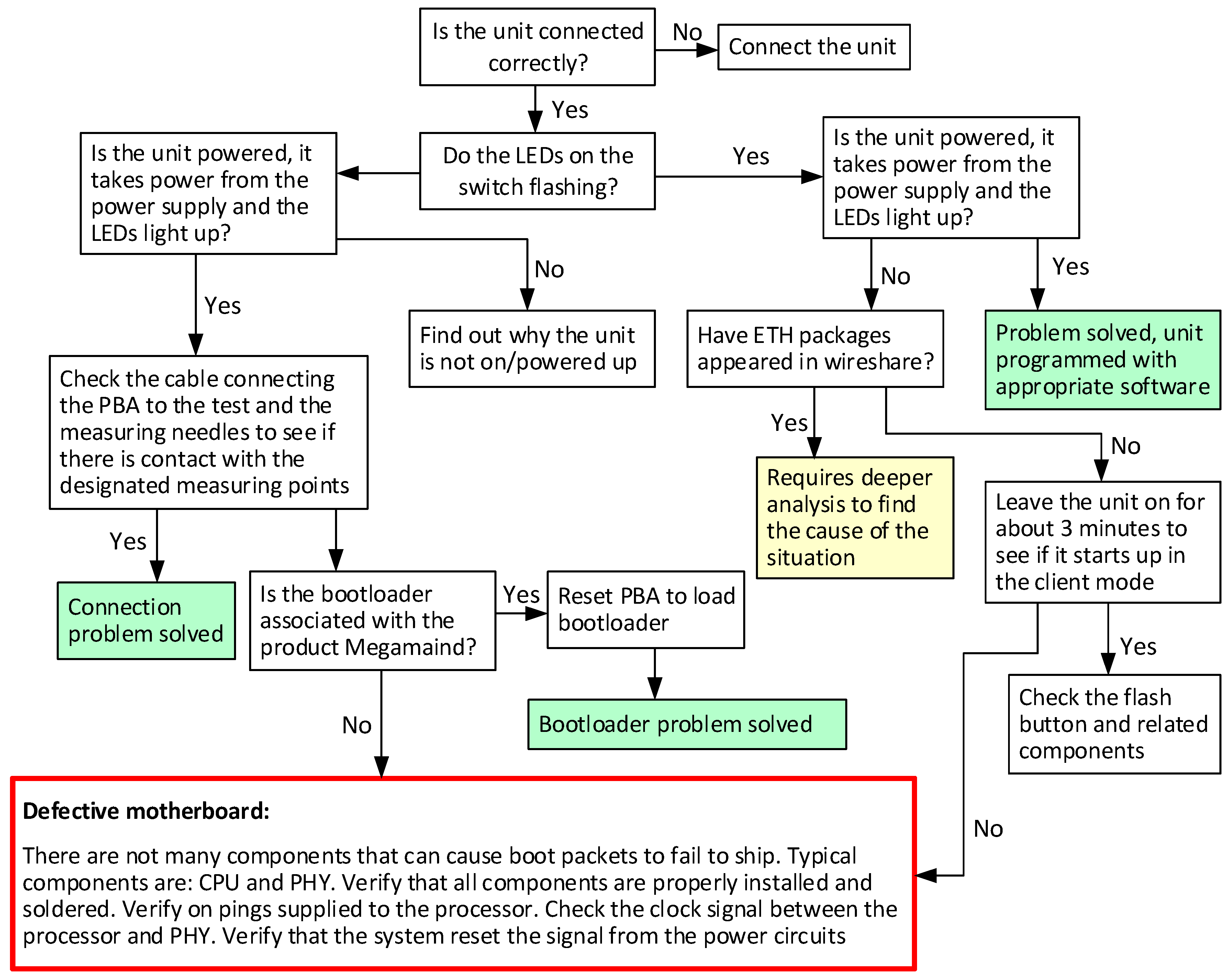
Each problem may have many causes and solutions. Therefore, based on measurements and numerous different experiences, a logical scheme of conduct is created for finding faults—a kind of repair manual. With reference to the previous example, the procedure can be described as a decision tree, as seen in the example shown in
Figure 7. This step-by-step documentation shows the logical course of action leading to the solution of the problem.
Referring to the presented diagram (
Figure 7), the first step in the analysis of an “ERROR CODE: Load Final/Test FW” failure is to check whether the product has been connected correctly, in accordance with the test instructions. If so, it should be verified that the LEDs in the module flash in a specific sequence. Depending on the result of this check, two different problems could occur. If the LEDs do not illuminate or if errors are seen in their flashing sequence, then key voltages may be missing. This necessitates checking the components and signals in the power supply. Troubleshooting and correcting the power supply area or connecting the power cables properly may resolve the problem.
If, instead, the LEDs do flash properly, this indicates that the system is properly powered. In this case, one must check if pressing the service button that activates the individual functions of the system continues to trigger subsequent test sequences. If it does and the subsequent test steps run correctly, the problem is resolved. However, if the button does not trigger the next test, the Ethernet’s function should be checked. For this high-speed interface, system designers must account for design recommendations for high-speed signals. For the tested module, if the situation does not improve after disconnecting the power supply and leaving a 3 min break before restarting the device, additional actions should be taken to verify the operation of individual functional modules in accordance with the checklist. The technical book includes additional recommendations for an in-depth check of individual components and signals.
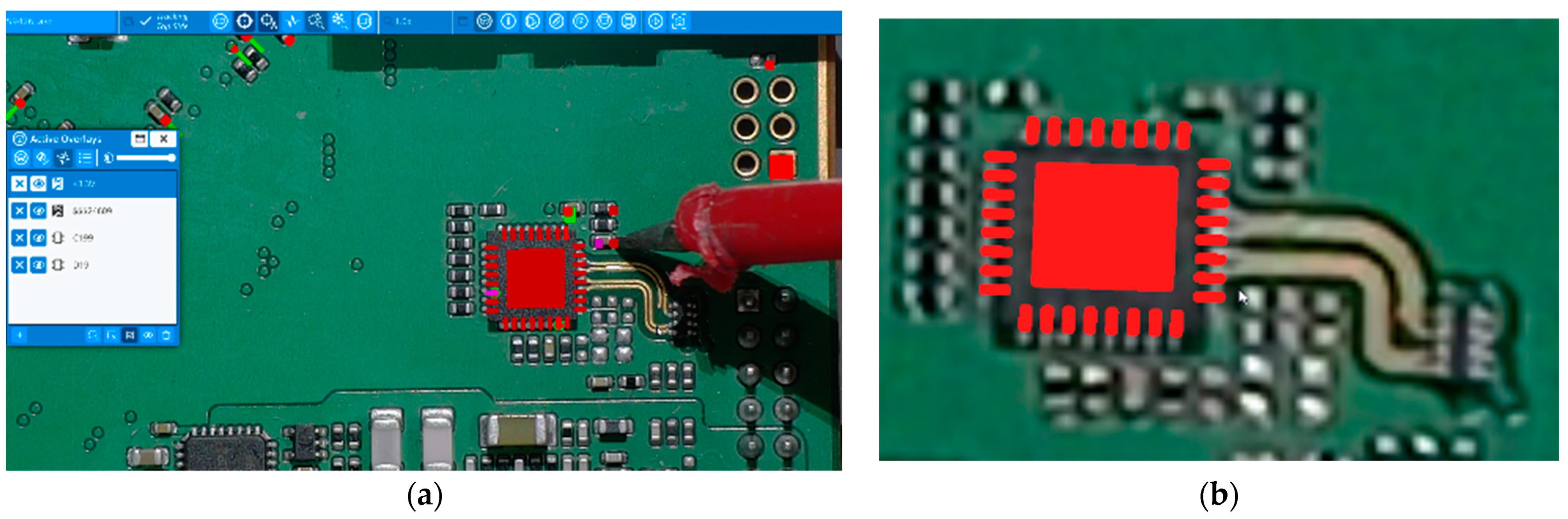
As illustrated in the example above, the debug analysis process may be complex and requires many pieces of information. InspectAR facilitates and simplifies this process. Referring to the individual steps of analyzing and debugging for the described problem, inspectAR facilitates the analysis of the PCBA circuit in augmented reality. By hovering the cursor over inspectAR’s virtual PCBA image presentation and then clicking the mouse button over a component, users can select and highlight the component and its attached nets (e.g., “X19” marked in
Figure 8). Alternatively, inspectAR can display a complete list of all components and nets, providing an alternate method for highlighting objects of interest (e.g., faulty components). Obtaining such an image is possible thanks to the use of a high-resolution 4 k camera.
Referring to the previously described debug steps, inspectAR enables the quick localization of components placed on the PCB laminate, which are interconnected by a network of electrical connections that are described by the names of individual signals. Some of the components that may be responsible for an “ERROR CODE: Load Final/Test FW” failure are those responsible for signals related to the operation of the Ethernet connection. They can be located by their names and colors may be assigned to them, as shown in
Figure 9a. One can also call up a list of Ethernet-related signal connections between individual components. There is one color for each different signal, such as the “red” shown in
Figure 9b. This color-based differentiation of transmitting signal connections is a feature of inspectAR.
The main advantage of the tool is that the design and component data can be seen displayed over the real product. Thus, one can see information from two sources (the design’s digital twin and the real board) in one place. This is a significant difference compared with the view of the electronic module that we get with the help of other PCB layout viewers.
An example of a tool similar to inspectAR is presented in
Figure 10. In this case, the PCB view does not account for or show the actual components used in the electronic circuit, but only their physical arrangement. So, while this tool does facilitate the physical localization of a component, one must separately inspect the PCBA and examine its components to discern their case type and supplier (especially for integrated circuits and BGAs).
Due to the use of an optical camera, inspectAR allows users to not only locate components on PCBAs, but also examine and replace the components without the need for a microscope. An example of component measurement using a probe aided by AR component visualization is shown in
Figure 11a. In this case, it is important to have a camera with the appropriate optical zoom to maintain image quality. The use of a 4k camera and software-only magnification in low optical magnification does not provide the required quality of PCB view (
Figure 11b). The camera quality (sensor resolution and optical zoom capabilities) directly impacts how well inspectAR functions, which in turn affects the quality of the data the end user sees. Therefore, it is important to use a high-quality camera.
Locating a potentially defective component ends with the decision to replace it and completing the final steps in the repair process (from 5 to 7 in
Table 1). The fix iteration will be repeated if retesting the module does not produce the expected “pass” result. As mentioned previously, there may be inaccuracy in diagnosing a fault’s cause, as one fault may have many potential causes. Hence, sometimes the diagnosis needs to be reassessed.
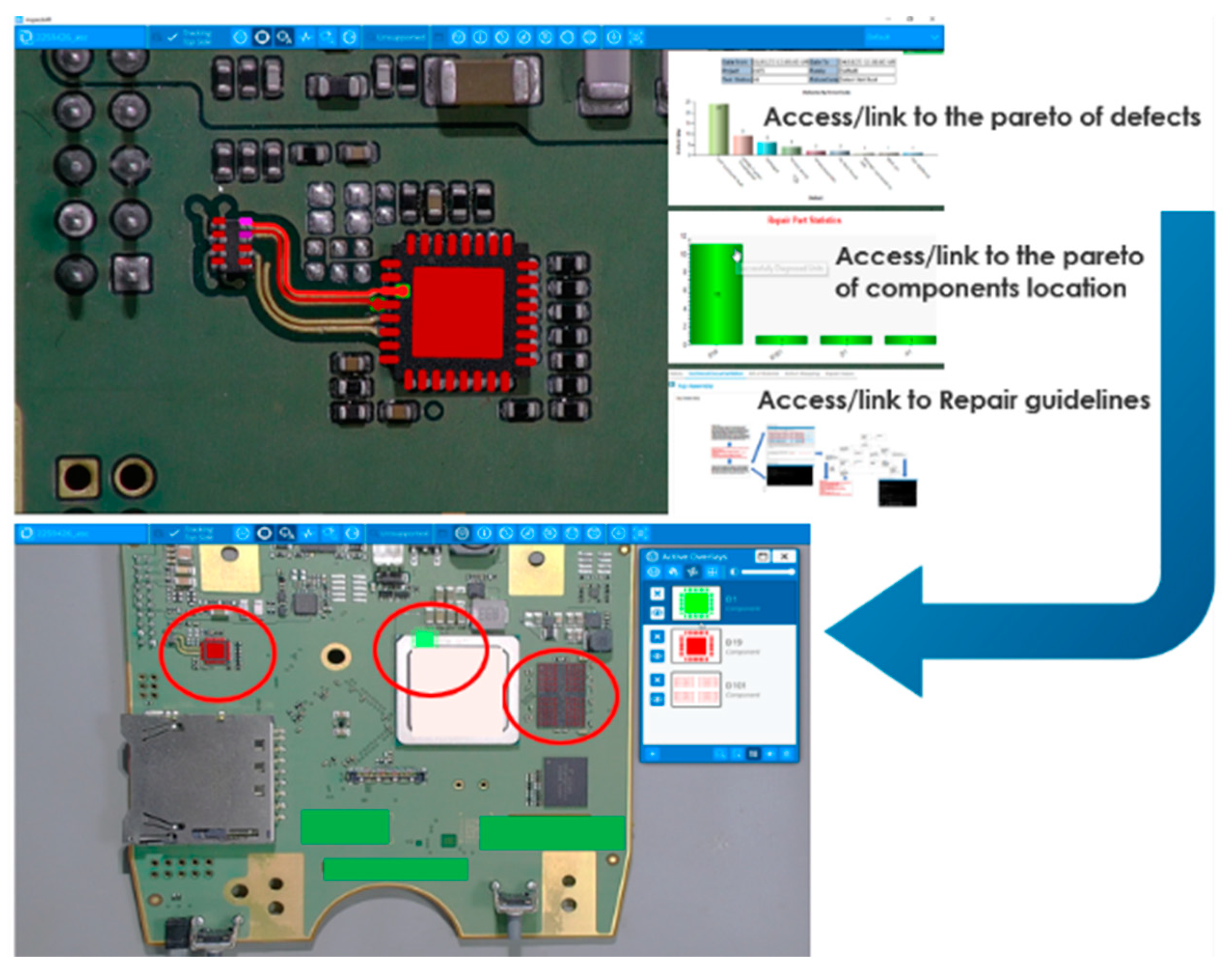
The development of inspectAR is expected to result in a tool that can be integrated with the manufacturer’s information systems, with easy access to the company’s database with a history of repairs and a Pareto chart of defects to enable a soft start in debugging any failures. In this vision, inspectAR will highlight components with a history of failure (
Figure 12). This way, the tool could provide even greater support for debuggers and faultfinders.
6. Conclusions
This article presents a new tool, inspectAR, dedicated to supporting the diagnostics process of electronic modules. Due to the use of an augmented reality solution, the process of finding damage can be much faster than using classical tools available on the market. The most important functionalities of inspectAR are described, and its usefulness is illustrated for a selected module.
InspectAR has many advantages that make analyses of real PCBAs much easier. The advantages of the elaborated system are mentioned below. This system quickly locates a component pin definition and components connected to a specific signal. It also quickly presents a potential failure/defect to someone without CAD files, displayed on the actual PCBA. The inspectAR application also assists in locating components and networks on complex PCBAs. The considered system assists repair operators in the early stages of production.
The presented tool is useful for test engineers/test designers during the debug phase. For unknown and complex PCB circuits, inspectAR is very useful. It gives the opportunity to probe live under a camera and see that the probe is in the right place. The inspectAR application can save technicians a lot of time by reducing or avoiding the need to search or study the PCB’s documentation. It also makes that documentation readily available should the user require it. The use of inspectAR provides an interactive way to analyze PCBs by combining high-resolution optical inspection with the integrated data of BOMs, schematics, and datasheets in the same software, which makes the diagnosis more efficient.
The presented diagnostic tool is still being developed and has opportunities for enhancement and extension. The areas of possible enhancement include: increased performance, deployment as a virtual appliance (VA), enhanced user interface/experience, a layout viewer mode, a customer-facing API, in-app procedure authoring, and broader support of data types and sources.
The proposed tool could be usable for many manufacturers of electronic modules. The use of this tool in industrial practice could notably reduce the time-consuming operations of debugging and repairing in the production process. The inspectAR application could increase production yield.


 ,
, 


