1. Introduction
In recent years, the development trend of wireless communication has been to utilize software radio to achieve functions of the digital domain for a transmitter. The all-digital transmitter (ADTx) has developed rapidly, and its flexible reconfigurable and programmable performance meets the design requirements of the high efficiency of the transmitter and the demand of SDR technology [
1,
2]. ADTx implements radio frequency (RF) functions such as up-conversion and pulse encoding in the digital domain and is mainly composed of a direct digital radio frequency modulator (DDRFM), a switched-mode power amplifier (SMPA), and the tuning filter. The DDRFM not only realizes the digital up-conversion of the baseband signal but also converts the digital radio frequency signal into a pulse signal suitable for switching amplification through a certain pulse encoding algorithm [
3].
Radio frequency pulse width modulation (RF-PWM) [
4] is one of the most commonly employed pulse encoding algorithms for an ADTx system. It can map the amplitude and phase of the input signal to the pulse width and position of the periodic pulse, respectively. In the ADTx system based on the RF-PWM algorithm, the outphasing architecture [
5,
6] is especially suitable. An example of such ADTx based on digital outphasing control and RF-PWM [
7] is provided in
Figure 1, which decomposes the input signal into two constant amplitude signals with different phases. Then, two outphasing signals drive independent switching power amplifiers, respectively, and synthesizes the output power RF signal.
At present, many various modulator architectures that combine outphasing and RF-PWM [
8,
9] have been proposed. Nevertheless, there is an important problem in practical applications when using the outphasing architecture for RF-PWM. Using only the time information of the pulse edge to encode amplitude and phase requires an extremely high time resolution, which also means that a higher sampling rate is required. The high sampling rate greatly increases the difficulty of digital signal processing [
10]. References [
11,
12] propose a multi-level RF-PWM scheme that increases the number of modulation pulse levels to improve performance. Due to the increase in amplitude resolution, the requirement for a time resolution is reduced with the desired performance. Nevertheless, the increase in the number of levels will inevitably lead to a more complex ADTx system. References [
13,
14,
15] used digital delay line chips to achieve high-resolution requirements. They used two outphasing signals separated from the baseband signal to drive the delay line chip to generate high-resolution pulse sequences. However, the modulator of this architecture requires devices with high-precision delay control, which brings higher requirements of implementation.
The outphasing architecture of ADTx for digital interpolation phase modulation has been proposed in [
16,
17]. Multiple DSPs simultaneously calculate the delay amount corresponding to the edge intersection point of the pulse signal to drive multiple parallel delay line chips. The output pulse sequences are synthesized into a high time resolution pulse. Nevertheless, this parallel architecture requires multiple devices with high-precision delay control, and this digital integrated ADTx also places higher requirements on implementation. The parallel outphasing architecture of ADTx based on RF-PWM has been proposed [
18]. By maintaining the outphasing signal separated from the baseband signal for
N carrier cycles and dividing it into
N channels for parallel processing, it effectively increases the sampling rate, but the phase error caused by the sample-and-hold method is large, which limits the quality of the output signal.
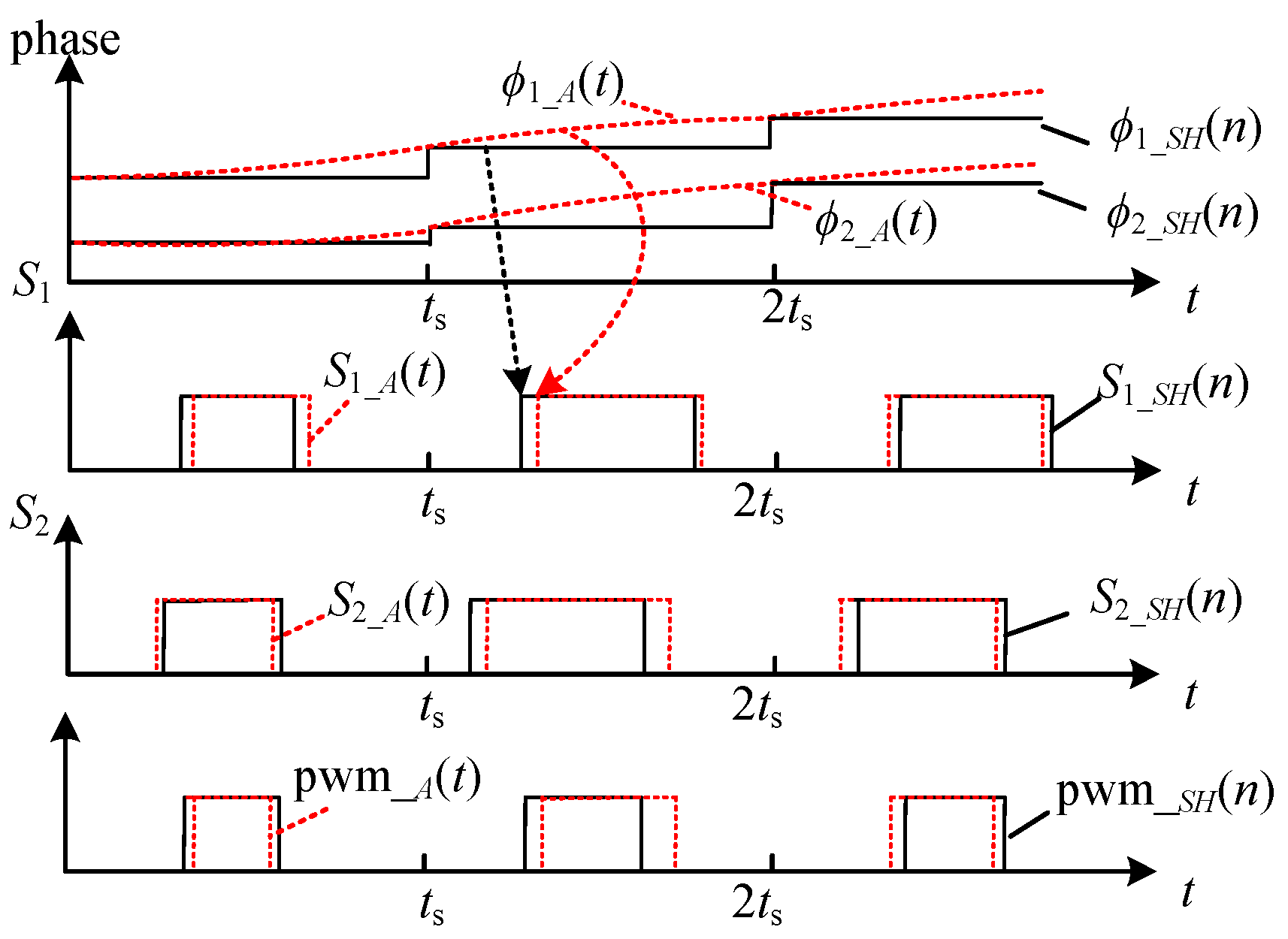
Figure 2 shows the error diagram of the modulation process of the outphasing control signal of analog
ϕx_A(
t) and sample-and-hold
ϕx_SH(
n).
Sx_A(
t) and
Sx_SH(
n) are outphasing modulated square waves, respectively. It can clearly be seen that the modulation coding output pwm_
SH(
n) corresponding to the sample-and-hold method deviates from the output pwm_
A(
t) of the analog signal. A parallel architecture based on RF-PWM for ADTx employed a method based on polyphase interpolation, which effectively improves the time resolution and reduces the processing rate [
19]. Meanwhile, the polyphase quadrature up-conversion and polyphase digital direct synthesis (DDS) used in this modulator architecture greatly increases the consumption of multiplier resources. In the encoding process, the polyphase triangular wave has not only a more cumbersome frequency selection but also causes the spectrum to contain more interfering harmonics.
Therefore, an outphasing architecture based on the parallel RF-PWM method for ADTx is proposed in this paper, which can increase the sampling rate while reducing the difficulty of signal processing and simplify the implementation structure. First, the polyphase interpolation filtering method is used to divide the two outphasing signals corresponding to the baseband signal into multiple paths. Then, the principle of zero-crossing comparison is used to implement parallel RF-PWM. The outphasing architecture is combined with the zero-crossing comparison principle to explore a method through angle calculation and quadrant judgment, which greatly simplifies the modulation and encoding process. Finally, parallel-to-serial conversion effectively increases the sampling rate and reduces the clock rate by MGT. Compared with existing parallel PWM technologies, the proposed scheme has significant advantages in terms of code efficiency (CE) and system complexity.
2. Outphasing Architecture Based on the Parallel RF-PWM Scheme
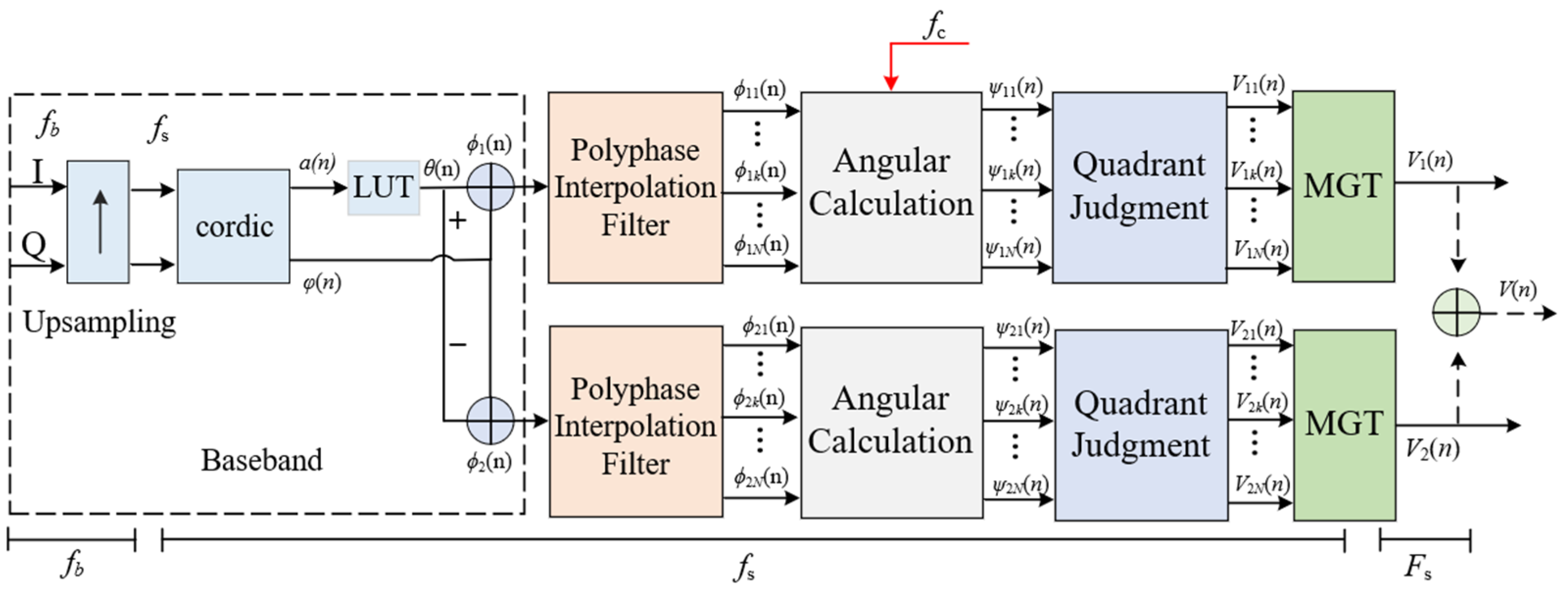
To avoid the impact caused by the sample-and-hold method, the interpolation filter is considered to reduce the error. Nevertheless, when up-conversion and pulse encoding are performed, the high sampling rate signal obtained by interpolation increases not only the difficulty of digital signal processing but also the power consumption of the FIR filter. Therefore, it is necessary to operate at a low sampling rate and small data amount. The polyphase interpolation filter method can reduce the processing rate and meet the requirements for real-time signal processing. Based on this, the proposed outphasing architecture based on the parallel RF-PWM method for ADTx is shown in
Figure 3. The architecture is mainly composed of the baseband module, polyphase interpolation filter module, parallel angle calculation, quadrant judgment module, and MGT module. Firstly, the amplitude and phase of the signal are extracted in the baseband module, and the outphasing angle is calculated to generate two corresponding outphasing phase signals, respectively. Then,
N-paths signals are obtained through the polyphase interpolation module and encoded in the parallel angle calculation and quadrant judgment modules. Next, the low-speed
N-path signals are combined into two high-speed binary signals with different phases through the MGT module, and the sampling rate is increased to
N times the baseband sampling rate. Finally, the two signals drive SMPAs, respectively, which generates a three-level output power signal.
2.1. Baseband Module
After the baseband IQ signal is up-sampled and the sampling rate
fb is raised to
fs, the amplitude
a(
n) and phase
φ(
n) of the signal are extracted by cordic. The corresponding outphasing angle
θ(
n) can be calculated through amplitude a(
n) according to Formula (1), which can be replaced by a lookup table to avoid consuming computing resources. The outphasing signals
ϕ1(
n) and
ϕ2(
n) are calculated, respectively, based on the outphasing angle and phase, as shown in Formula (2):
2.2. Polyphase Interpolation Filter Module
First of all, the transmission function
H(
z) of the digital filter is decomposed into several groups of different phases, and the
z transformation of the filter
h(
n) is:
where the tap coefficients
h(
n) are divided into
N groups, and
L is the number of filter orders, which is an integer multiple of
N. Then, the polyphase decomposition of
H(
z) can be obtained as [
20]:
Also, in this case
where
M =
L/
N should be an integer. Formula (4) is called the polyphase decomposition of
H(
z). Polyphase decomposition is used to divide the prototype filter into multiple low-order sub-filters, and the order of each sub-filter is only 1/
N of the original. All branches of a polyphase filter are all-pass filters with a phase difference of 1/
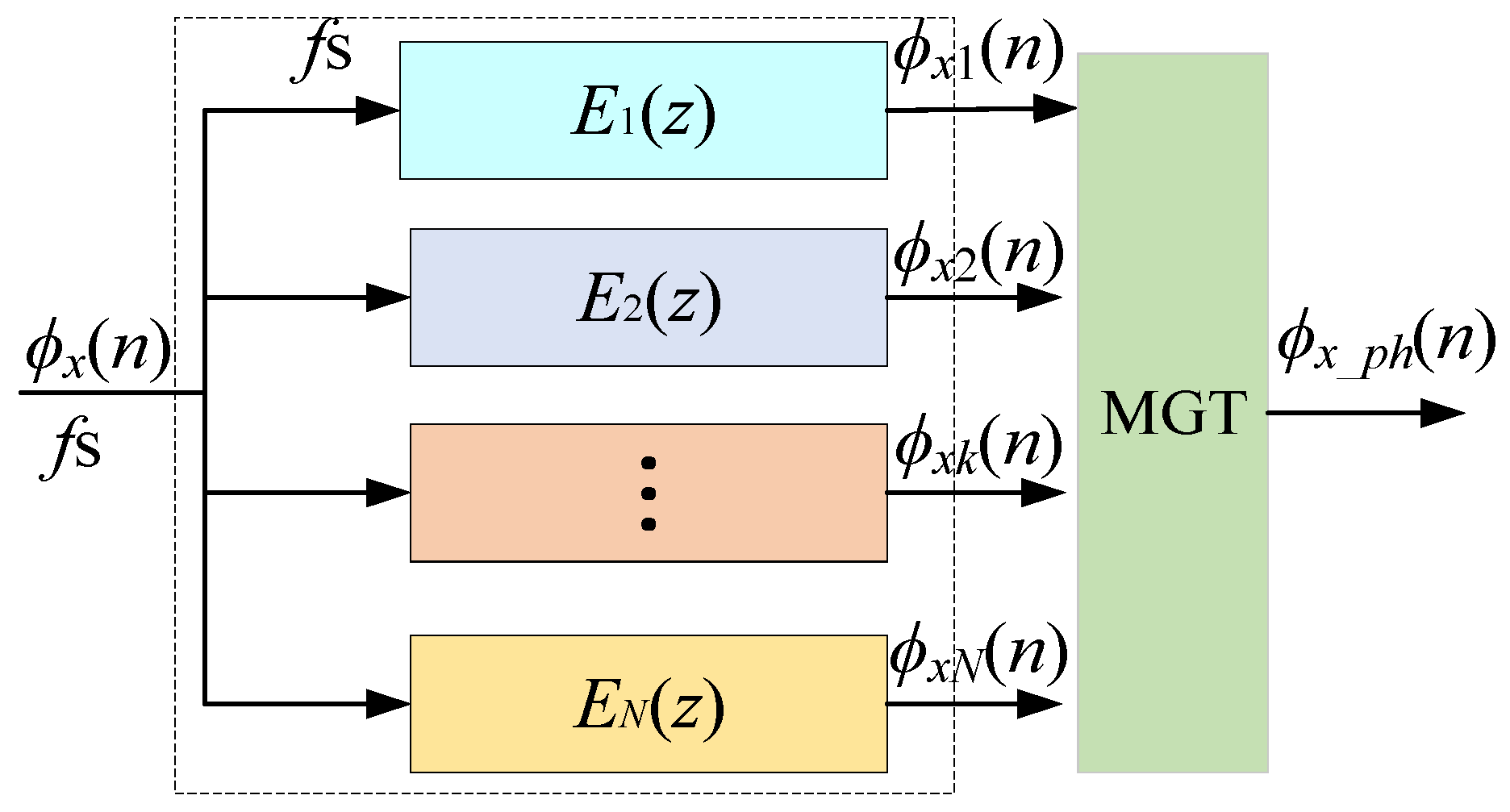
N between the neighboring branch filters. Polyphase filtering divides the transfer function of the digital filter into several branches of different phases according to the phase equalization relationship. Thus, the structure of the polyphase interpolation filter is shown in
Figure 4. The input is the outphasing signal
ϕxk(
n) (
x = 1, 2 and
k = 1, 2, …,
N). The polyphase interpolation filtering part has
N paths. The parallel output phase signals on adjacent paths are time continuous. If other subsequent processing is not considered, the equivalent high-speed outphasing signal
ϕx_ph(
n) can be obtained by directly converting the parallel outphasing signal through the MGT.
A comparison diagram of the modulation of the analog outphasing signal
ϕx_A(
t) and the equivalent outphasing signal
ϕx_ph(
n) is shown in
Figure 5. According to the phase comparison, the curves of
ϕx_ph(
n) and
ϕx_A(
t) are very close, and the corresponding modulated square waves
Sx_A(
t) and
Sx_pp(
n) are close to overlap. Therefore, the error between the final synthesized pulse width modulation sequences pwm_
A(
t) and pwm_
pp(
n) is extremely small. Compared with the sample-and-hold method, the generated phase error is greatly reduced, and the quality of the output encoded signal is significantly improved in this polyphase interpolation filtering method.
2.3. Angle Calculation and Quadrant Judgment Module
For the outphasing signals ϕ
1k (
n) and ϕ
2k(
n) (1 ≤
k ≤
N) output by the polyphase interpolation filter in parallel, according to the original formula of outphasing, the phase modulation signal calculation formula of parallel outphasing is derived as Formula (6):
where
k is the
k-th path of the polyphase interpolation filter output, and
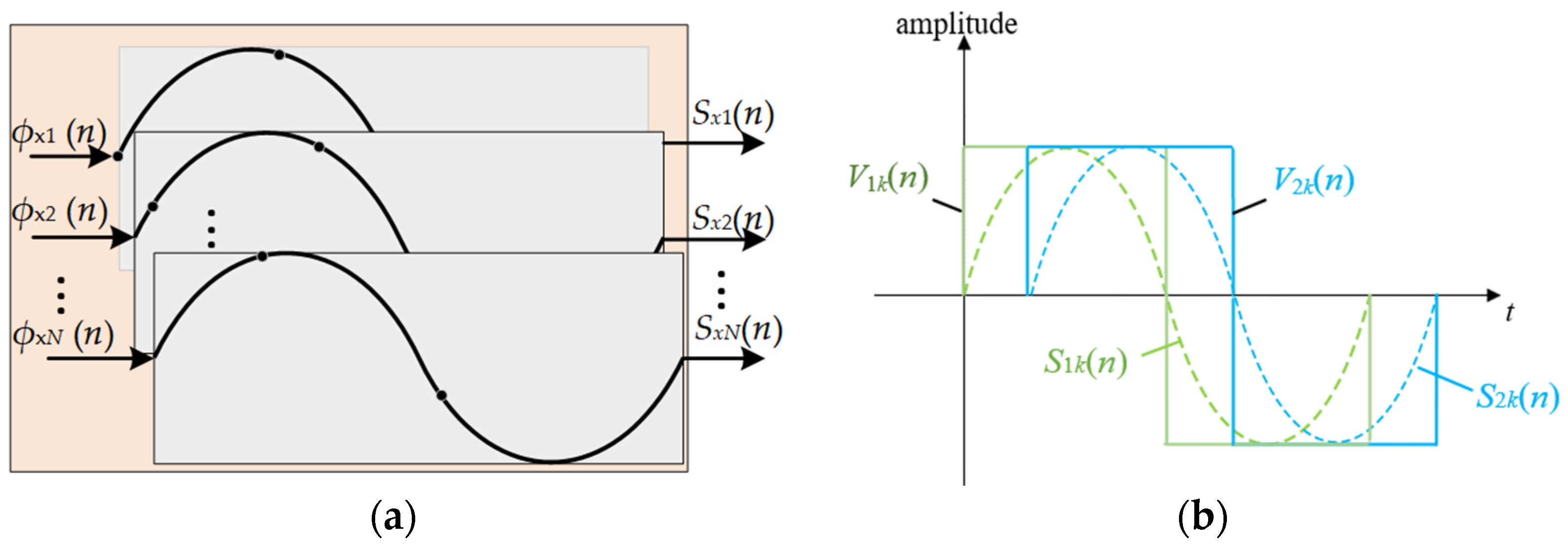
n is the number of discrete time points. The output diagram of the parallel phase modulation signal
Sxk(
n)(
x = 1,2) is shown in
Figure 6a, and the input is outphasing signal
ϕxk (
n) (
x = 1,2). The phase difference in the adjacent branch is 1/
N, and the sampling rate of each branch is 1/
N of
Fs. In order to obtain the low words width coded signal, it is necessary to perform RF-PWM on parallel modulated signals. For the
k-th path, RF-PWM needs to be performed on the above corresponding modulation signal. As shown in
Figure 6b, according to the zero-crossing comparison process, the two-level square wave sequences
V1k(
n) and
V2k(
n) with different phases are generated according to the positive and negative signs of the modulation signals
S1k(
n) and
S2k(
n). Therefore, it can be considered to directly generate a two-level pulse sequence by judging the quadrant of the cosine function angle in Formula (6). Then, pulse encoding and up-conversion is achieved.
Therefore, the main part of the angle calculation in
Figure 3 is shown in Equation (7).
where
ψ1k(
n) and
ψ2k(
n), respectively, represent the angle value of the
k-th path cosine function in Formula (6). According to the properties of the cosine function, when the angle value
ψ1k(
n) is in the first and fourth quadrants, the cosine value is more than zero, and the corresponding output level is +1. When
ψ1k(
n) is in the second and third quadrants, the cosine value is less than zero, and the corresponding output level is 0, and the binary pulse sequence in the
k-th path can be generated.
Therefore, by simply judging the quadrant of the angle, the parallel RF-PWM of the outphasing architecture can be realized. Since the ranges of ψ1k(n) and ψ2k(n) are uncertain, the quadrant cannot be directly determined. In order to facilitate judgment, the angle is classified into the (−π, π) interval, and the quadrant judgment is made after the processing angle. This method can complete the frequency up-conversion and pulse encoding of the signal only through simple angle calculation and quadrant judgment, which greatly simplifies the implementation of the system and reduces the computational complexity.
2.4. MGT Module
In Xilinx FPGA, MGT integrates a high-speed parallel-to-serial conversion (PISO) function, which can convert low-speed parallel data into high-speed serial data. Therefore, after parallel modulation and coding, the output low-speed parallel pulse sequences
V1k(
n) and
V2k(
n) are converted into parallel-to-serial, respectively, through the MGT module to generate two high-speed two-level pulse sequences. Taking
V1k(
n) as an example, the diagram of the parallel-to-serial conversion output is shown in
Figure 7. It can be seen that the signals of adjacent branches are logically continuous in time, and the serial rate
Fs is
N times the parallel rate
fs. The two 1-bit high-speed output pulse sequences by the parallel-to-serial conversion are synthesized into the final target high-speed three-level pulse sequence through the SMPA.
3. Simulation and Analysis
In order to explore the performance impact of the sub-filter order
K on the architecture proposed in this paper, the simulation uses a 16QAM modulated signal with a baseband sampling rate
fb of 50 MHz and a bandwidth of 20 MHz, and the carrier frequency
fc is 200 MHz. Polyphase FIR filter coefficients are generated by Blackman window.
Figure 8 shows the changing trend of ACPR and EVM values as the sub-filter order
K changes when
N is set to 16, 32, 64, and 128, respectively. As shown in the figure, the change in
K has a significant influence on ACPR and EVM. When the sub-filter order
K increases, ACPR and EVM have a gradually decreasing trend and gradually level off after
K = 4. When
N takes different values, the performance curve always maintains this pattern. When
K is less than four, the poor performance index is due to the fact that the filter order is too low, resulting in the filtering processing not being able to achieve the ideal effect.
Figure 9 shows the impact of sub-filter order changes on performance when the signal bandwidth is 5 MHz. It can be seen that the output performance curve converges faster when the bandwidth is lower. The change trends in
Figure 8 and
Figure 9 are similar, so when the bandwidth is small, the impact of changes in
K on performance indicators can maintain the same trend as when the bandwidth is large. During the implementation process, the increase in the sub-filtering order will lead to an increase in the consumption of computing resources. Therefore, in order to balance the system performance and the consumption of computing resources,
K is selected as four as the optimal value.
In order to explore the impact of the number of parallel paths
N on performance, when
N takes different values, the changes in the output spectrum and performance indicators are analyzed. The simulation selects a 16QAM modulation signal with a baseband sampling rate
fb of 50 MHz and a bandwidth of 20 MHz as the input. The carrier frequency
fc is 200 MHz, and the baseband signal is up-sampled four times to 200 MHz.
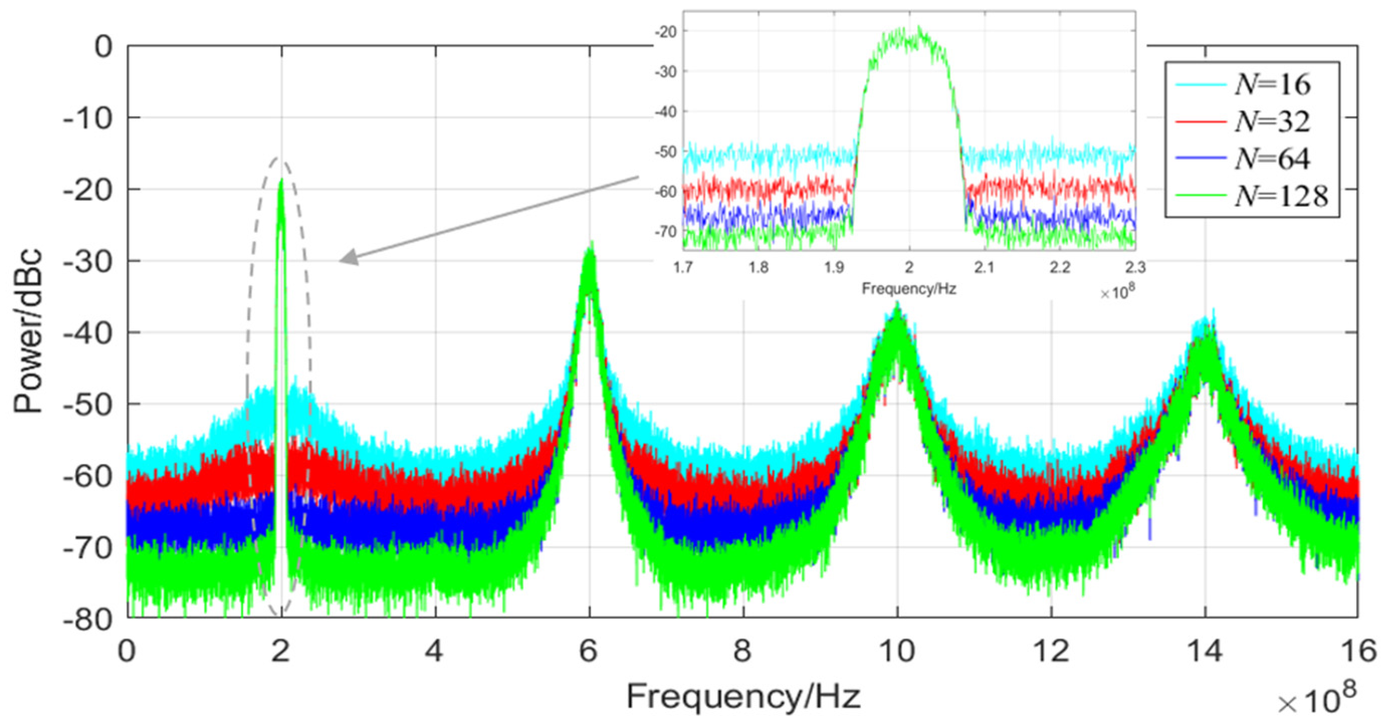
Figure 10 shows the spectrum diagram when the number of parallel paths
N is set to 16, 32, 64, and 128, respectively. It can clearly be seen that as
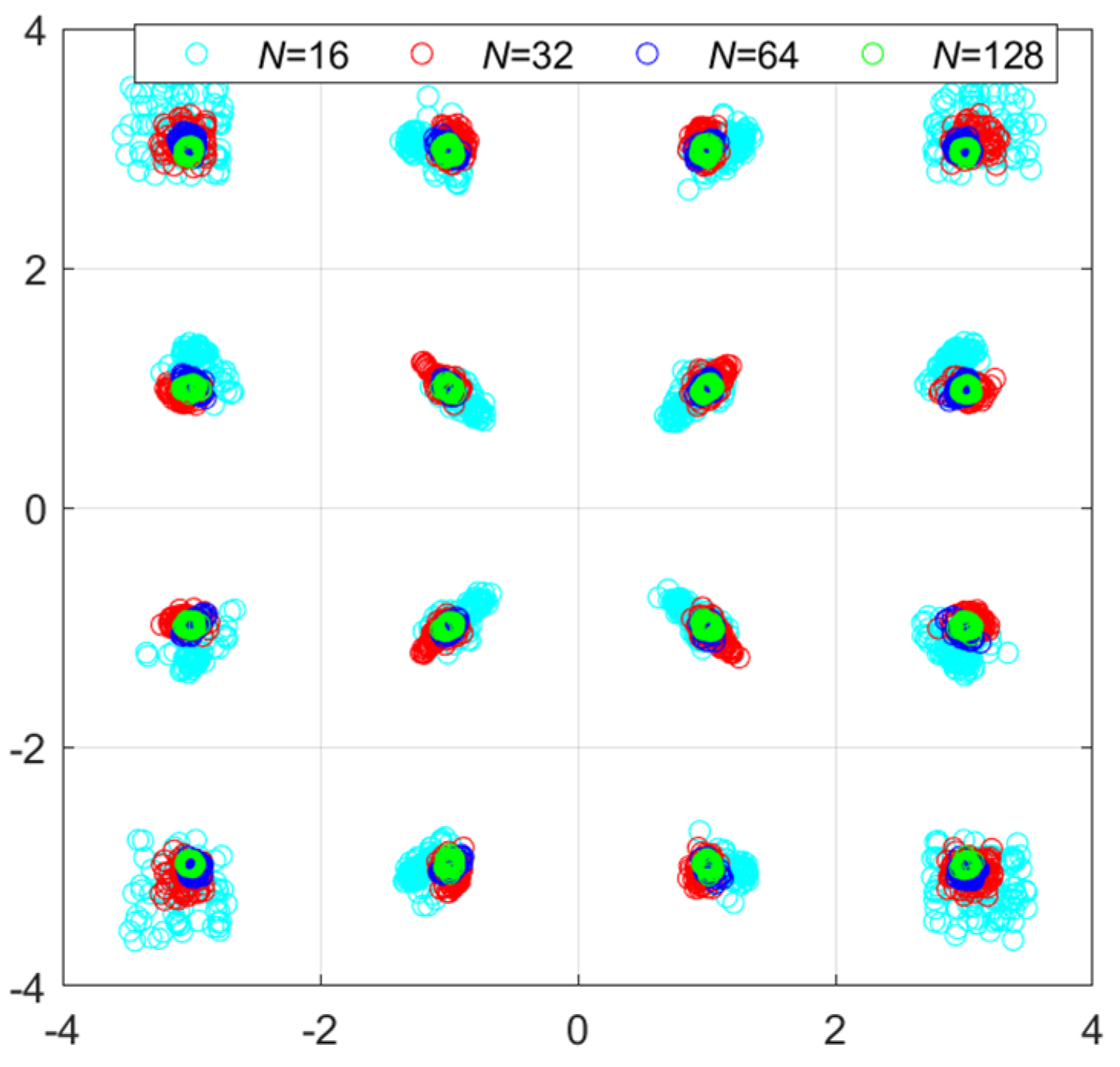
N increases, the noise floor and in-band noise of the spectrum gradually decrease, and the ACPR obtained gradually increases. After filtering out the unwanted out-of-band signals, the original signal is restored through the demodulation. The corresponding demodulated constellation diagrams when
N takes different values is shown in
Figure 11. The values of EVM are 9.1%, 4.0%, 1.7%, and 0.9%, respectively. It can be seen that as
N increases, the distribution of the constellation diagram gradually becomes concentrated, and the EVM obtained gradually decreases. Nevertheless, the increase in
N will lead to enhanced resource consumption, and it is necessary to balance output performance and resource consumption.
Figure 12 shows the changing trend of the output performance index when
N takes different values. It can be seen that the output performance indicators have similar changing trends when the signal bandwidth is 5 MHz and 20 MHz. The increase in the number of parallel paths
N has a significant impact on the optimization of ACPR and EVM. However, after the number
N exceeds a certain value, the decline becomes slow. CE is less affected by
N, and it remains basically unchanged with the increase in
N. For input signals with different bandwidths, the narrower the bandwidth, the better the obtained ACPR and CE performance is. However, the change in bandwidth has a smaller improvement in EVM.
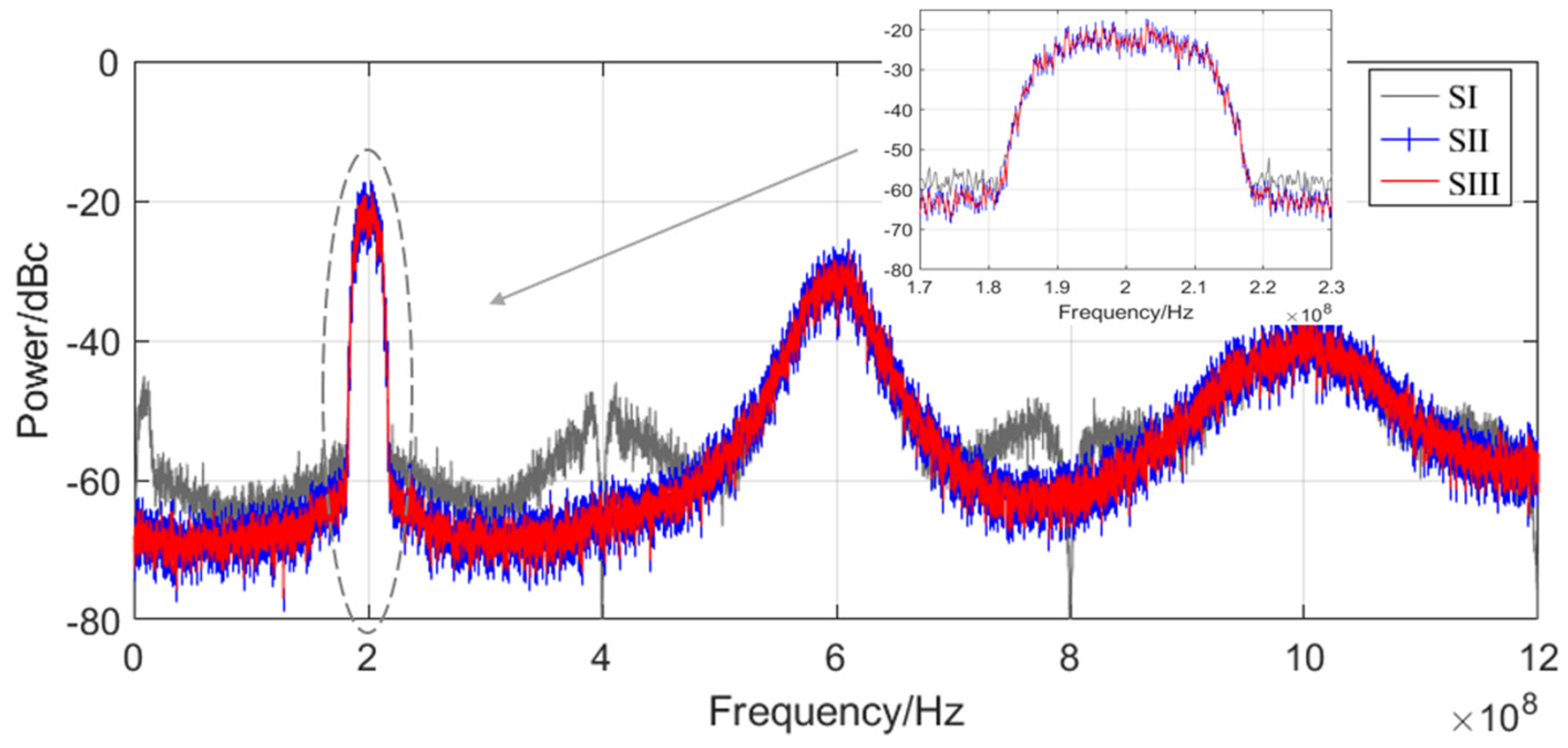
The simulation spectrum diagrams of schemes SI, SII, and SIII with 20 MHz bandwidth is shown in
Figure 13. SI is the architecture proposed in [
18], SII is the architecture proposed in this paper, and SIII uses a high sampling rate to achieve single path outphasing architecture. The baseband conditions selected for simulation are equal to the above, and the value of
N is 128. The sampling rate of the parallel branch of schemes SI and SII is 200 MHz, and the final sampling rate of the parallel-to-serial conversion output is 25.6 GHz. The final sampling rate of SIII is the same with both. From
Figure 12, it can be concluded that the simulated spectra of SII and SIII are basically consistent. Nevertheless, since the signal is processed in a single path in scheme SIII, high-speed digital signal processing is difficult to achieve. Therefore, the advantage of using the proposed architecture is to convert high-rate single-channel digital signal processing into multiple low-rate paths for parallel processing. The filtering operation is also performed on the decomposed low-order sub-filters, which greatly reduces the digital signal processing difficulty. As shown in
Figure 12, compared with scheme SI, scheme SII has a better improvement in ACPR value. In addition, since scheme SI adopts the principle based on sample-and-hold, its quantization error is larger than scheme SII at the same resolution. Otherwise, even-order harmonics appear, which has a greater impact on signal quality. The ACPR for SII and SIII stands at −46.5 dBc, while for SI it is −41.3 dBc in this situation.
Figure 14. presents simulated spectral graphs for schemes SI, SII, and SIII when the baseband bandwidth is set to 40 MHz. It can clearly be observed from the graph that if other conditions remain unchanged, an increase in width will lead to a decrease in ACPR. The ACPR obtained from the SII is −39.4 dBc. In order to achieve the same performance as when the bandwidth is 20 MHz, it is necessary to enhance the rate of parallel processing or to increase the number of parallel paths. This means that a higher rate of parallel-to-serial conversion is required.
In this architecture, by decomposing high-order filters into multiple low-order sub-filters, the hardware implementation complexity is reduced, and the working frequency is lowered to 1/N of the original frequency. In terms of algorithm complexity, the classical outphasing implementation algorithm is transformed into polyphase implementation, eliminating the need for complex calculation steps and the classical quadrature up-conversion stage. The polyphase processing algorithm will also not require complex hardware circuits in the subsequent implementation plan. Moreover, the outphasing-based architecture is relatively simple and conducive to building an all-digital transmitter. Regarding resource utilization complexity, it is expected to be deployed and implemented using FPGA and will not consume excessive resources. Preliminary estimations suggest that the main resource consumption may be due to the use of multipliers in the polyphase interpolation filter module, which may require a certain amount of DSP resources.
Table 1 compares the output performance of this scheme with other parallel schemes. Compared with the method in [
21], the CE of the proposed scheme is improved about 20%. And the use of DSM involved in [
21] increases the complexity of the system. Compared with the method in [
18], the proposed scheme improves both ACPR and EVM, which means that the restriction on the number of paths is relaxed while ensuring the output performance. Although the scheme in [
19] shows better ACPR and EVM, it requires the use of polyphase digital direct synthesis (DDS) for quadrature up-conversion and uses polyphase triangle wave signals during encoding, which greatly increases resource consumption. In the modulation part, compared with these three schemes, the proposed method greatly simplifies the up-conversion and pulse encoding.

