Abstract
Wireless Power Transfer (WPT) can effectively solve the problem of autonomous power supply for low-power devices. Rectifier is the key component in WPT technology. In this paper, a novel impedance matching network for the broadband rectifier is proposed. This impedance matching network compensates for the diode impedance and reduces its impedance change when the frequency or input power changes. The passive boosting mechanism utilizing coupled transmission lines (CTLs) improves the power conversion efficiency (PCE) of the diode in the low power region. The structure is especially optimized for low-power device applications. For validation, a broadband rectifier operating at 1.9–3 GHz is fabricated and measured. The structure fabricated on the Rogers 4003 substrate with a thickness of 1.508 mm and the diode is HSMS2860. The DC voltage on the load ( Ω) was measured. The results show that at 0 dBm, the PCE keeps more than 60% at 1.98–3 GHz. The peak PCE of 79.6% is obtained at 4 dBm. The compact size of the broadband rectifier is 19 mm × 21 mm. This broadband rectifier for low input power ranges can be applied to WPT technology.
1. Introduction
Wireless power transmission (WPT) has received increasing attention as it enables powering devices over long distances [1,2,3]. The rectifier is an important part of determining the power conversion efficiency (PCE) of the WPT system. High PCE and compactness are research priorities in the design of rectifiers [4,5].
In recent years, many rectifiers have been proposed. These works have focused on single-band [6,7,8,9] and multi-band rectifiers [10,11,12,13,14]. The structure presented in Ref. [6] achieves PCE of more than 80% at 2.45 GHz at 25 dBm. A multi-band rectifier with a single impedance matching network is proposed by Halimi et al. [10]. A single-band rectifier is first designed and then converted to dual-band and tri-band by adding transmission lines (TLINs). The structure can work at common bands such as 1.95 GHz and 5.8 GHz. A dual-band rectifier is suggested in Ref. [11]. Using a half-wavelength transmission line (HWTL) in the matching network to increase the operational band. At 3.5 GHz and 5.8 GHz, the PCE is 42.3% and 54.9%, when the input power is 0 dBm. However, most of these structures show narrow-band characteristics and low PCE in other operational bands. Some broadband rectifiers have been designed [15,16,17,18,19,20]. The 1.6–3.0 GHz range covers many applications such as WIFI, 4G, ISM, and other applications. In Ref. [15], a two-stage impedance matching network is proposed. PCE over 70% from 1.80 to 2.72 GHz at 19.5 dBm. The broadband rectifier presented by He et al. Ref. [16] achieves PCE more than 70% at 2.1–3.3 GHz with an input power of 14 dBm. A compact wideband rectifier is proposed in Ref. [20]. The structure consists of a multilayer printed circuit board. The center frequency is 12.795 GHz and the fractional bandwidth is 40.33%.
However, these structures are not suitable for low input power. Since the input voltage to the diode must be greater than the threshold voltage in order for the diode to start, the diode loss is the biggest limiting factor in the rectifier circuit’s inability to achieve high efficiency at low input power. In order to improve the PCE at low input power, studies have been carried out in Refs. [21,22]. Ref. [21] enhances PCE by increasing the efficiency of each part of the rectifier and by using a low-loss dielectric substrate and reducing diode losses. Ref. [22] achieves high pce by controlling the diode temperature and lowering the threshold voltage.
Coupled transmission lines (CTLs) have been shown in studies to have the effect of expanding the bandwidth [23] and filtering out the harmonics [24]. In this paper, we use additional properties of CTLs. CTLs are combined with TLINs to realize impedance matching over a wide frequency band. On the other hand, CTLs realize passive voltage enhancement, effectively increase the RF signal voltage amplitude loaded on the rectifier diode, and improve the diode forward conduction time and reducing diode losses, which improves the PCE at low power levels. For verification, a broadband rectifier operating at 1.9–3 GHz is fabricated and measured. The structure fabricated on the Rogers 4003 substrate with a thickness of 1.508 mm and the diode is HSMS2860. The DC voltage on the load ( Ω) was measured. According to the measurement result, the PCE reaches more than 40% from 1.9 to 3 GHz with a bandwidth of 44.9% at −10 dBm. The RF-DC conversion efficiency of the rectifier remains above 60% with a bandwidth of 41% from 1.98 to 3 GHz at 0 dBm. At 4 dBm, the highest measurement efficiency is 79.6%.
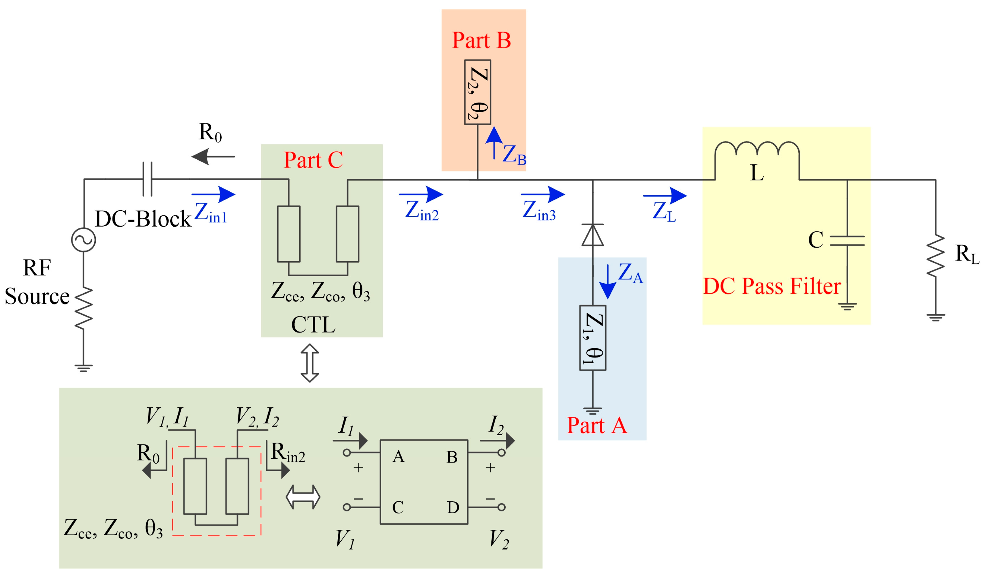
2. Broadband Rectifier Design and Analysis
Figure 1 shows the schematic diagram of the proposed broadband rectifier, which consists of three main parts. The design of these three parts is described specifically next. The DC pass filter can be realized in the conventional method.
Figure 1.
The proposed broadband rectifier.
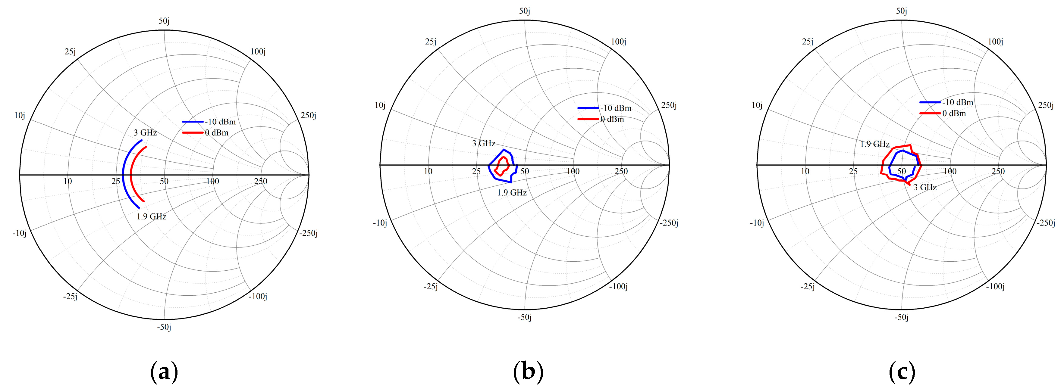
2.1. Design of Part A
Part A consists of a transmission line. This part realizes the conjugate matching of the input impedance at the lowest and highest frequencies. The lowest and highest operating frequencies within the wideband are denoted as and , respectively. The frequency ratio of and is (). The input impedance at and is expressed as:
TLINs labeled as TL1-TL2. The characteristic impedance and electron length of the TL1 are and . can be expressed as follows using transmission line theory:
and are defined as the electrical length at two frequencies, respectively. can be expressed as:
At and , making the real parts of equal and the imaginary parts are opposite to each other. Thus the impedance at and is realized conjugate:
It follows from (2–5) that
From (6) and (7), the parameters of TL1 can be solved as:
Part A can be verified by calculating and . As shown in Figure 2a, on a wideband is calculated using the impedance change formula. The real part of is about 30. The imaginary part is essentially symmetrical at the center frequency.
Figure 2.
Design principles of the broadband input impedance matching network: (a) Design A; (b) Design B; (c) Design C.
2.2. Design of Part B
Part B consists of an open stub with characteristic impedance and electrical length . This part is used to eliminate the imaginary part of and keep the real part unchanged. The input impedance of can be expressed as:
According to part A, at and can be expressed as follows:
To eliminate the imaginary part of by adding an open stub:
From (13) and (14) calculate and :
is defined as:
The results show that the real part of and are the same and the imaginary part is close to 0. Figure 2b shows the performance of in the Smith Chart for different input power levels. The curves are close to the real axis and are compressed within a smaller region. The part C realizes further matching of the source impedance with the diode input impedance.
2.3. Design of Part C
Part C consists of a CTL. The coupling of two transmission lines results from the interaction of their respective electromagnetic fields when they are in close proximity. The coupling effect varies at different frequencies. Since the imaginary part of is zero, only the real part of needs to be considered. CTLs have more design freedom because they have many design parameters. The can be changed during the design process by adjusting the width, gap distance and electrical length of the CTL. Impedance matching is realized in two frequencies according to Ref. [25]. Then, they are matched and adjusted within the bandwidth. Figure 1 shows a schematic diagram of the parameters of the CTL. The matrix of the CTL can be expressed as:
At and , is converted to by a CTL.
is the source impedance of the rectifier. The CTL parameters , , can be solved by (18–22):
After obtaining the initial parameters of the CTL and further fine-tuning is performed using ADS simulation software to get a better match on the wideband. The input impedance is obtained by part C as shown in Figure 2c. The curves remain essentially the same at −10 dBm and 0 dBm, indicating that the rectifier can operate over a wide input power range.
At low power input, the load voltage of the rectifier is introduced along the DC path to the diode. When the of the diode is less than or equal to the of the diode, the diode is not turned on because there is not enough energy. According to Ref. [26], a new CTL-based design criterion is used in order to boost the of the diode.
represents the voltage gain by introducing a CTL. Substituting the values obtained from (23–25) into (26) obtains . This passive voltage boost is used to augment the input voltage, thereby increasing the dc voltage across the diodes.
The design parameters of the proposed structure are obtained from the derivation. To facilitate the rectifier processing, the actual physical lengths and widths are provided in Table 1.
Table 1.
Design parameters for the broadband rectifier.
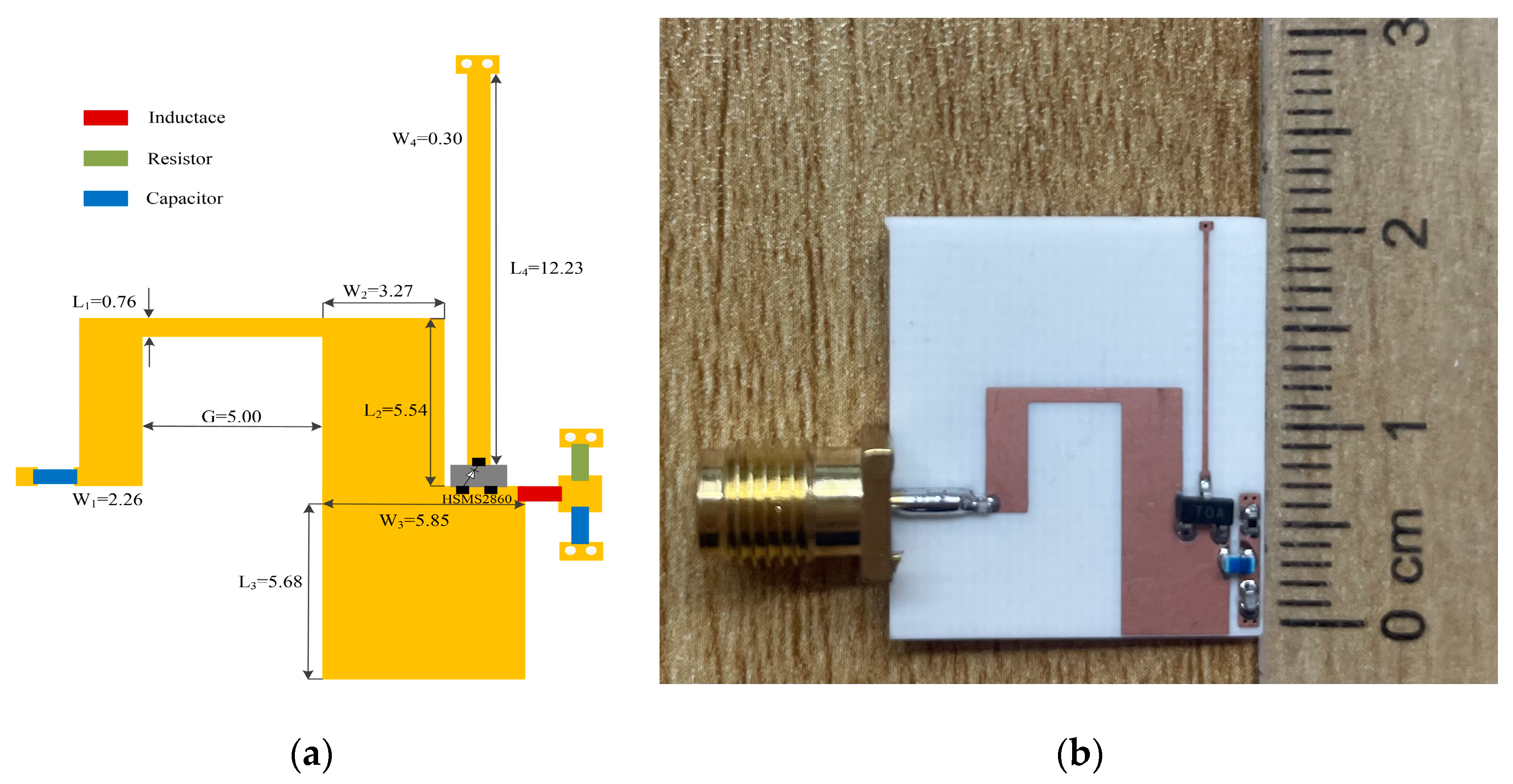
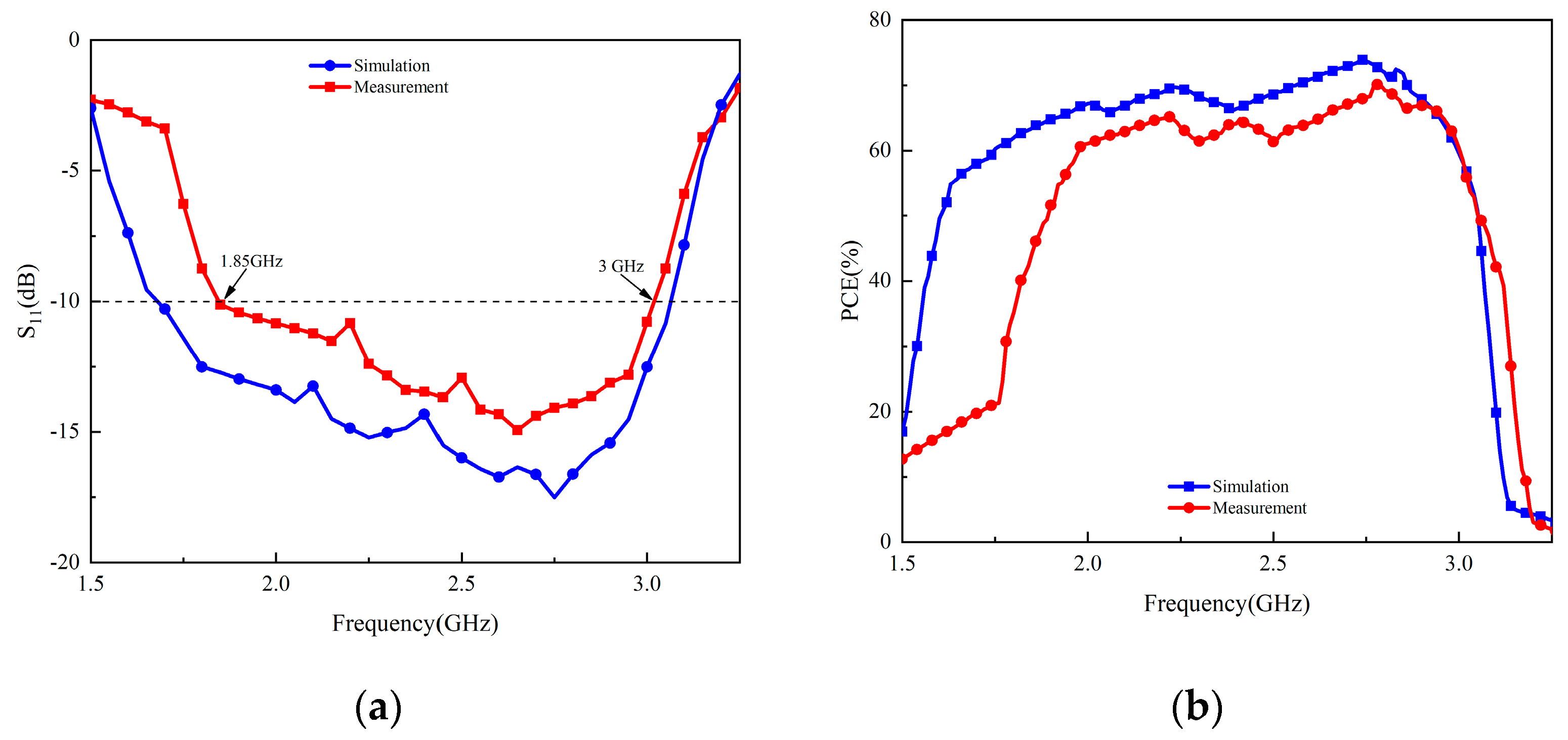
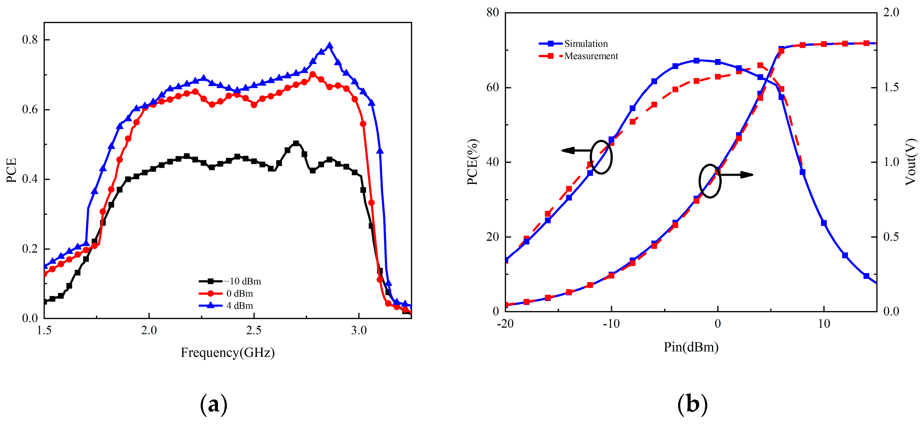
3. Implementation and Experimental Results
For verification, a broadband rectifier is designed. The structure fabricated on the Rogers 4003 substrate (Rogers Corporation, Chandler, AZ, USA) (tanδ = 0.0027, ) with a thickness of 1.508 mm and the diode type is the Schottky diode HSMS2860. The DC voltage on the load ( Ω) was measured by varying the input power and frequency. The DC-block capacitor is 24 pF. The DC-pass filter consists of a 5 nH inductor and a 24 pF capacitor. Figure 3a shows the layout of the rectifier. Figure 3b shows the fabricated rectifier.
Figure 3.
(a) Layout of the proposed rectifier; (b) Fabricated rectifier.
PCE is the ratio of output power to input power, which is represented as:
where Vout is DC out voltage, RL is the load, Pout is output power, and Pin is input power.
Simulated and measured input return loss (S11) at 0 dBm. As shown in Figure 4a, S11 is less than −10 dB from 1.85 GHz to 3.0 GHz, which shows the structure performs well over a wideband. The rectifier of the PCE versus frequency at 0 dBm is shown in Figure 4b. The simulated and measured results are essentially identical. In the wide band range of 1.98–3 GHz, the PCE is over 60% and the bandwidth is 41%. The difference between simulated and measured results may be due to processing errors and diode losses.
Figure 4.
(a) Simulated and measured S11 at the input power of 0 dBm; (b) Simulated and measured PCE versus frequency at the input power of 0 dBm.
The PCE versus frequency for different input power levels is shown in Figure 5a. When the input power is −10 dBm, the PCE remains above 40% in the range of 1.9–3 GHz. When the input power is 0 dBm, the PCE remains above 60% in the range of 1.98–3 GHz. The PCE keeps above 70% in the range of 1.97–2.95 GHz at 4 dBm. The broadband rectifier performance is further analyzed. Effect of input power variation on PCE and output voltage when 2.45 GHz is selected in the wide band. The simulation and measurement results are shown in Figure 5b. Input power range from −8.5 dBm to 7 dBm at 2.45 GHz when PCE over 50%. The measured conversion efficiency is 45.1% at −10 dBm. Output voltage is 240 mV. At 0 dBm, the conversion efficiency is 62.9% and the output voltage is 932 mV. The peak PCE of 79.6% is obtained at 4 dBm with an output voltage of 1.43 V.
Figure 5.
(a) Measured PCE versus frequency with different input power from −10 to 4 dBm; (b) Simulated and measured PCE and Vout versus input power at 2.4 GHz.
Table 2 shows the performance comparison with existing works. The 1.6–3 GHz covers most of the applications, so wideband rectifiers in this range are chosen for comparison. Compared to the existing works, the proposed rectifier has a wide band in the low input power range and maintains the compact size of 19 mm × 21 mm.
Table 2.
Performance comparison with the state-of-the-art broadband rectifiers.
4. Conclusions
In this paper, we propose a novel impedance matching network based on CTLs. Impedance matching is achieved by utilizing the design freedom of a single CTL in combination with TLINs. And by realizing greater than 1, it extends the dynamic voltage of the input signal and ensures the conversion efficiency at low power. The design of a broadband rectifier at low input power is realized by this method. For verification, a broadband rectifier is fabricated and measured. The measured results show that at −10 dBm, the PCE keeps more than 40% at 1.9–3 GHz with a bandwidth of 44.9%. When the input power is 0 dBm, PCE above 60% and the bandwidth is 41% at 1.98–3 GHz. The structure is more compact than existing rectifiers and maintains a high PCE over a wide-band.
Author Contributions
Conceptualization, Y.L.; Validation, Y.L.; Writing—original draft, Y.L.; Writing—review & editing, G.X. All authors have read and agreed to the published version of the manuscript.
Funding
This research was funded by the Key Research and Development Plan of Shanxi Province, grant number 202102020101002.
Data Availability Statement
The raw data supporting the conclusions of this article will be made available by the authors on request.
Conflicts of Interest
The authors declare no competing interests. The funders had no role in the design of the study; In the collection, analyses, or interpretation of data; in the writing of the manuscript; or in the decision to publish the results.
References
- Shinohara, N. Trends in wireless power transfer: WPT technology for energy harvesting, mllimeter-wave/THz rectennas, MIMO-WPT, and advances in near-field WPT applications. IEEE Microw. Mag. 2021, 22, 46–59. [Google Scholar] [CrossRef]
- Huang, J.; Zhou, Y.; Ning, Z.; Gharavi, H. Wireless power transfer and energy harvesting: Current status and future prospects. IEEE Wirel. Commun. 2019, 26, 163–169. [Google Scholar] [CrossRef] [PubMed]
- Muhammad, S.; Tiang, J.J.; Wong, S.K.; Smida, A.; Ghayoula, R.; Iqbal, A. A dual-band ambient energy harvesting rectenna design for wireless power communications. IEEE Access 2021, 9, 99944–99953. [Google Scholar] [CrossRef]
- He, Z.; Lin, H.; Zhu, H.; Liu, C. A compact high-efficiency rectifier with a simple harmonic suppression structure. IEEE Microw. Wirel. Compon. Lett. 2020, 30, 1177–1180. [Google Scholar] [CrossRef]
- Liu, C.; Tan, F.; Zhang, H.; He, Q. A novel single-diode microwave rectifier with a series band-stop structure. IEEE Trans. Microw. Theory Techn. 2017, 65, 600–606. [Google Scholar] [CrossRef]
- He, Z.; Lin, H.; Liu, C. A novel class-C rectifier with high efficiency for wireless power transmission. IEEE Microw. Wirel. Compon. Lett. 2020, 30, 1197–1200. [Google Scholar] [CrossRef]
- Surender, D.; Halimi, M.A.; Khan, T.; Talukdar, F.A.; Antar, Y.M.M. A 90° twisted quarter-sectored compact and circularly polarized DR rectenna for RF energy harvesting applications. IEEE Antennas Wirel. Propag. Lett. 2022, 21, 1139–1143. [Google Scholar] [CrossRef]
- Aldhaher, S.; Yates, D.C.; Mitcheson, P.D. Load-independent class E/EF inverters and rectifiers for MHz-switching applications. IEEE Trans. Power Electron. 2018, 33, 8270–8287. [Google Scholar] [CrossRef]
- Du, Z.X.; Zhang, X.Y. High-efficiency microwave rectifier with less sensitivity to input power variation. IEEE Microw. Wirel. Compon. Lett. 2017, 27, 1001–1003. [Google Scholar] [CrossRef]
- Halimi, M.A.; Surender, D.; Khan, T.; Kishk, A.A.; Rengarajan, S.R. A multistepped transmission line matching strategy based triple-band rectifier for RFEH/WPT applications. IEEE Microw. Wirel. Compon. Lett. 2022, 32, 1007–1010. [Google Scholar] [CrossRef]
- Halimi, M.A.; Khan, T.; Koul, S.K.; Rengarajan, S.R. A dual-band rectifier using half-wave transmission line matching for 5G and Wi-Fi bands RFEH/MPT applications. IEEE Microw. Wirel. Compon. Lett. 2023, 33, 74–77. [Google Scholar] [CrossRef]
- Li, S.; Cheng, F.; Gu, C.; Yu, S.; Huang, K. Efficient dual-band rectifier using stepped impedance stub matching network for wireless energy harvesting. IEEE Microw. Wirel. Compon. Lett. 2021, 31, 921–924. [Google Scholar] [CrossRef]
- Yue, Z.; Xu, X.; Li, S.; Zhu, Y.H.; Lin, X.Q. Efficient and compact tri-band rectifier with large frequency ratio for WPT. IEEE Microw. Wirel. Compon. Lett. 2022, 32, 1355–1358. [Google Scholar] [CrossRef]
- Wang, S.H.; Zheng, S.Y.; Leung, K.W.; Xia, M.H. A self-matched multi-band rectifier for efficient electromagnetic energy harvesting. IEEE Trans. Circuits Syst. I Reg. Papers 2021, 68, 4556–4565. [Google Scholar] [CrossRef]
- Li, L.F.; Yang, X.; Liu, E.J. A broadband high-efficiency rectifier based on two-level impedance match network. Progr. Electromagn. Res. Lett. 2018, 72, 91–97. [Google Scholar] [CrossRef]
- He, Z.; Liu, C. A compact high-efficiency broadband rectifier with a wide dynamic range of input power for energy harvesting. IEEE Microw. Wirel. Compon. Lett. 2020, 30, 433–436. [Google Scholar] [CrossRef]
- Mansour, M.; Mansour, I.; Zekry, A. A reconfigurable class-F radio frequency voltage doubler from 650 MHz to 900 MHz for energy harvesting application. Alex. Eng. J. 2022, 61, 8277–8287. [Google Scholar] [CrossRef]
- Gyawali, B.; Thapa, S.K.; Barakat, A.; Yoshitomi, K.; Pokharel, R.K. Analysis and design of diode physical limit bandwidth efficient rectification circuit for maximum flat efficiency, wide impedance, and efficiency bandwidths. Sci. Rep. 2021, 11, 19941. [Google Scholar] [CrossRef]
- Liu, L.; Zhang, P.; Weng, M.H.; Tsai, C.Y.; Yang, R.Y. A Miniaturized Wideband Bandpass Filter Using Quarter-Wavelength Stepped-Impedance Resonators. Electronics 2019, 8, 1540. [Google Scholar] [CrossRef]
- Li, C.; Ma, Z.H.; Chen, J.X.; Wang, M.N.; Huang, J.M. Design of a Compact Ultra-Wideband Microstrip Bandpass Filter. Electronics 2023, 12, 1728. [Google Scholar] [CrossRef]
- Zhang, Y.; Shen, S.; Chiu, C.Y.; Murch, R. Hybrid RF-solar energy harvesting systems utilizing transparent multiport micromeshed antennas. IEEE Trans. Microw. Theory Tech. 2019, 67, 4534–4546. [Google Scholar] [CrossRef]
- Gu, X.; Guo, L.; Hemour, S.; Wu, K. Optimum temperatures for enhanced power conversion efficiency (PCE) of zero-bias diodebased rectifiers. IEEE Trans. Microw. Theory Tech. 2020, 68, 4040–4053. [Google Scholar] [CrossRef]
- He, H.; Lin, H.; Wu, P.; Li, Q.; Liu, C. Compact high-efficiency broadband rectifier based on coupled transmission line. IEEE Trans. Circuits Syst. II Exp. Briefs 2022, 69, 4404–4408. [Google Scholar] [CrossRef]
- Zhao, F.; Inserra, D.; Wen, G. Compact and high efficiency rectifier design based on microstrip coupled transmission line for energy harvesting. In Proceedings of the IEEE/MTT-S International Microwave Symposium, Los Angeles, CA, USA, 4–6 August 2020. [Google Scholar]
- Wu, Y.; Sun, W.; Leung, S.; Diao, Y.; Chan, K.H. A novel compact dual-frequency coupled-line transformer with simple analytical design equations for frequency-dependent complex load impedance. Progr. Electromagn. Res. 2013, 134, 47–62. [Google Scholar] [CrossRef]
- Zhao, F.; Inserra, D.; Gao, G.; Huang, Y.; Li, J.; Wen, W. High-Efficiency Microwave Rectifier with Coupled Transmission Line for Low-Power Energy Harvesting and Wireless Power Transmission. IEEE Trans. Microw. Theory 2021, 69, 916–925. [Google Scholar] [CrossRef]
- Nguyen, D.A.; Seo, C. Design of high-efficiency broadband rectifier with harmonic control for wireless power transfer and energy harvesting. IEEE Microw. Wirel. Compon. Lett. 2022, 32, 1231–1234. [Google Scholar] [CrossRef]
- Wu, P.; Huang, S.Y.; Zhou, W.; Yu, W.; Liu, Z.; Chen, X.; Liu, C. Compact high-efficiency broadband rectifier with multistage transmission line matching. IEEE Trans. Circuits Syst. II Exp. Briefs. 2019, 66, 1316–1320. [Google Scholar]
- Bui, G.T.; Nguyen, D.A.; Seo, C. A highly efficient design of broadband rectifier with harmonic suppre ssion transferring for energy harvesting and wireless power transfer. IEEE Microw. Wirel. Compon. Lett. 2023, 33, 1059–1062. [Google Scholar] [CrossRef]
Disclaimer/Publisher’s Note: The statements, opinions and data contained in all publications are solely those of the individual author(s) and contributor(s) and not of MDPI and/or the editor(s). MDPI and/or the editor(s) disclaim responsibility for any injury to people or property resulting from any ideas, methods, instructions or products referred to in the content. |
© 2024 by the authors. Licensee MDPI, Basel, Switzerland. This article is an open access article distributed under the terms and conditions of the Creative Commons Attribution (CC BY) license (https://creativecommons.org/licenses/by/4.0/).