Article

Digital Active EMI Filter for Smart Electronic Power Converters

by
Michele Darisi
1,*,
Tommaso Caldognetto
1,*,
Davide Biadene
1 and
Marco Stellini
2
1
Department of Management and Engineering (DTG), University of Padova, 36100 Vicenza, Italy
2
Department of Information Engineering (DEI), University of Padova, 35131 Padova, Italy
*
Authors to whom correspondence should be addressed.
Electronics 2024, 13(19), 3889; https://doi.org/10.3390/electronics13193889
Submission received: 2 August 2024 / Revised: 10 September 2024 / Accepted: 28 September 2024 / Published: 30 September 2024

Abstract

:
Electronic power converters are widespread and crucial components in modern energy scenarios. Beyond mere electrical energy conversion, their electronic structure allows several functionalities to be naturally embedded in them, including energy management, diagnosis, communication, etc. The operation of the converter itself, or the system interfaced by the same, commonly produces undesired electromagnetic interferences (EMIs) that should comply with prescribed limits. This paper presents a digital active EMI filter designed to mitigate such disturbances. The proposed hardware implementation can acquire and analyze the common-mode (CM) noise affecting the circuit and inject a compensation signal to attenuate the measured interference. A novel adaptive algorithm is introduced to compute the necessary signals for effective noise cancellation. The implementation is integrated within a single printed circuit board interfaced with a field-programmable gate array (FPGA) running the control algorithm. The digital filter’s efficacy in EMI reduction is demonstrated using a synchronous buck converter with gallium nitride (GaN) power devices, achieving significant noise reduction. Additionally, potential functionalities are envisioned to fully exploit the capabilities of the proposal beyond EMI filtering, like fault detection, predictive maintenance, smart converter optimization, and communication.

1. Introduction

Power electronics play a pivotal role in today’s energy management, ensuring high efficiency and compact solutions that make this technology widely used in several applications. The evolution of Industry 4.0 sets new challenges towards the design of smarter systems, capable of collecting data from the field and exploiting this information to improve the operation of the system. In this paper, a digital electromagnetic interference (EMI) filter and related control algorithm is proposed that measures the undesired interference and actively attenuates the interference by injecting suitable compensation signals.
In general, EMI filters are being researched because wide-bandgap devices (WBDs), like power switches based on GaN or SiC, enable efficient switching at higher frequencies and high power density implementations [1]. Smaller parasitic and higher saturation velocities allow WBDs to switch faster, causing EMI interference on a wider spectrum compared to their Si counterparts [2]. In order to comply with EMI compatibility standards, passive filters are used to limit the noise produced by converters. These filters often occupy a considerable portion of the overall converter volume, representing one of the biggest and heaviest elements of the converter not directly involved in the conversion of energy. An example of a design that combines good performance and minimum volume of the filter is shown in [3]. Moreover, passive filters typically show very limited flexibility, because any changes require dedicated tuning and hardware modifications.
Active EMI filters (AEFs) have been developed aiming at reducing the size of passive filters for common-mode (CM) or differential-mode (DM) noise. Such filters combine an injection and a sensing circuit with active components like operational amplifiers or transistor amplifiers using discretes. The noise is sensed, amplified following a specific control law, and injected back to compensate the original signal. AEF topologies are classified as feedback or feed-forward, depending on the location of the injected signal; a generalized analysis is shown in [4]. AEFs used in combination with passive filters allow smaller passive elements, which helps reduce volumes while maintaining high attenuation. This kind of filter is referred to as a hybrid EMI filter; some examples and topologies are presented in [5,6].
The proper compensation of AEFs is based on a strong matching between the noise and the compensation signal, for this reason changes in the system impedance or in the gain of the filter due to parasitics can lead to instabilities and require additional compensation networks, as shown in [7].
Considering the periodic operation of electronic converters, it is possible to use the Fourier transform to break down the noise in the sum of sine waves and generate a cancellation signal that properly combines with the noise components. Based on this principle, digital active EMI filters (DAEFs) have been proposed [8,9,10]. By these filters, the noise is sampled, a control algorithm is applied, and a compensation signal is generated and injected synchronously with the operation of the converter. In this way, it is possible to apply additional algorithms to estimate online changes in impedance or delays in the system and accurately tune the cancellation signal, but also implement functions like health monitoring for preemptive maintenance or to demodulate signals carrying information [11,12]. One of the first implementations of a DAEF was reported in [9], where the digital filter was combined with a passive one. A good example of how harmonic cancellation is performed in a stationary clocked system is provided in [13], where an adaptive algorithm is applied. The algorithm is employed to initiate the optimization process closer to the optimal values by mapping the transfer function from injection to sensing. Subsequently, a scaled-down module is implemented, and the phase of the injected harmonics is optimized online. This approach prevents overcompensation and achieves a more efficient distribution of the available output power of the DAEF across the compensation band. A more detailed explanation of this method is provided in Section 2. Active EMI filters have also been proposed in the form of integrated circuits, like the TPSF12C1-Q1 by Texas Instruments [14]. Such a device is compact and capable of good noise reduction up to 3 M Hz . In general, DAEFs present good performance in the low-to-mid-frequency range, the proposed solution has been tested up to 10 M Hz , but as shown in [8], with powerful enough hardware it is possible to compensate the full range of conducted EMI, from 150 k Hz to 30 M Hz . Achieving noise reduction in the lower frequencies is especially relevant because passive filters are less efficient or bulky in this range.
Table 1 reports representative EMI filter implementations and briefly reports their main features.
In this paper, a DAEF is proposed composed of a sensing stage, a computation stage, and an injection stage. The hardware implementation is integrated into a single printed circuit board that exploits wide-bandwidth operational amplifiers, analog-to-digital converters, and digital-to-analog converters for the implementation of EMI sensing and the injection of the compensation signal. A digital control algorithm is also proposed and deployed on a field-programmable gate array (FPGA). By exploiting the hardware used for the EMI filter, the proposal can leverage the computing power of digital control architectures of future smart systems (e.g., smart inverter) to implement additional future functionalities in addition to noise reduction, like fault detection, predictive maintenance, and converter optimization. In fact, the generated interference is affected by the state of health and mode of operation of the converter. In the case of silicon carbide devices, some studies show a correlation between degradation and EMI noise [17,18,19]; these changes in the spectrum could be detected in order to prevent failure of the converter. The main contributions of this paper can be summarized as:
  • An algorithm that integrates an online adaptive optimization;
  • A hardware solution to implement the DAEF in a single board, reporting the selected components for signal acquisition and injection;
  • Discussions on perspectives for advanced features that can be supported by DAEFs embedded in smart electronic power converters.
The remainder of the paper is structured as follows. Section 2 presents the general structure and operating principle of the considered DAEF. The proposed control algorithm for the computation of the compensation signals is described in Section 3, while its implementation is reported in Section 4. Section 5 reports the operation of the implemented DAEF by means of experimental results in the frequency and in the time domains. Finally, Section 6 concludes the paper.

2. General Structure and Operating Principle of a DAEF

This section describes the fundamental blocks and basic principles of operation of a DAEF.

2.1. Fundamental Blocks

Figure 1 displays the basic scheme of a DAEF connected to an equipment under test (EUT). It is composed of three stages, namely, a noise extractor, a processing stage, and a compensation signal injection stage. To sense the noise extracted from the power supply lines it is possible to use different approaches, whether the compensation is performed based on current or voltage quantities; a complete list of the most used ones is reported in [20]. Voltage sensing can be easily performed using two high-pass filters, referred to as the protective earth (PE) conductor, and then, adding or subtracting the filtered noise in order to obtain common-mode or differential-mode components, as shown in [21]. The filter’s lower cutoff frequency is set sufficiently low so as to not alter frequency components higher than 150 k Hz . The compensation signal is injected through an R C branch. The capacitor value should be high enough to ensure sufficient coupling at low frequencies, but also limited to bound the current flowing to PE. In this application, a trade-off value of 6.8 n F is used.

2.2. Operating Principle

The working principle revolves around the principle of destructive interference between an EMI and a suitably designed compensation signal. The noise generated by a converter operating in steady state is periodic with frequency f 0 ; therefore, it can be described as the sum of harmonics at a frequency multiple of the fundamental:
v n o i s e ( t ) = k = 1 + | V n o i s e ( k f 0 ) | cos 2 π k f 0 t + θ k , θ k = V n o i s e ( k f 0 )
The noise sensed by the noise extractor is the superposition of the noise produced by the EUT and the signal injected by the DAEF, for the generic k-th component of the spectrum:
V s e n s e ( k f 0 ) = H ( k f 0 ) V i n j ( k f 0 ) + G ( k f 0 ) V n o i s e ( k f 0 )
In which H ( k f 0 ) is the transfer function that correlates injection with sensing, as stated below:
H ( k f 0 ) = V s e n s e ( k f 0 ) V i n j ( k f 0 ) | V n o i s e = 0
Meanwhile, G ( k f 0 ) describes the relationship between the noise generated by the EUT and sensed by the system:
G ( k f 0 ) = V s e n s e ( k f 0 ) V n o i s e ( k f 0 ) | V i n j = 0
The ideal cancellation signal to be injected can be obtained by imposing V s e n s e ( k f 0 ) = 0 for each harmonic of the spectrum, obtaining (5)
V i n j ( k f 0 ) = G ( k f 0 ) V n o i s e ( k f 0 ) H ( k f 0 )
This principle is also used in [8], attaining good results, under the assumption of knowing the transfer function from injection to sensing, which is crucial for accurate cancellation. Herein, an adaptive compensation is devised to overcome the errors performed during the mapping of the transfer function.

3. DAEF Control Algorithm

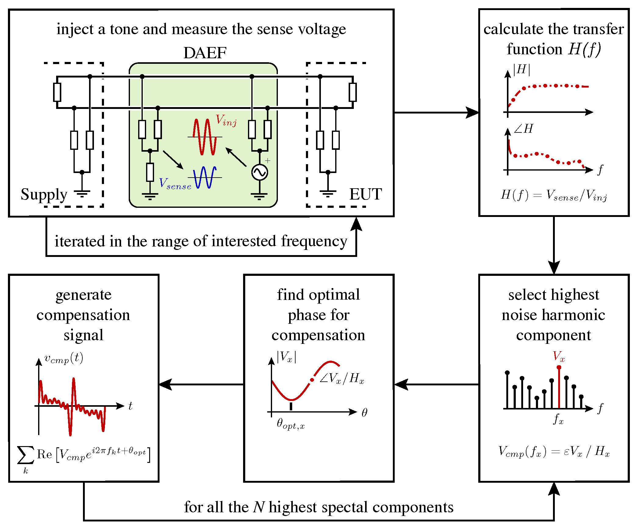
Figure 2 shows the flowchart of the control algorithm proposed for the developed DAEF. The algorithm is based on an adaptive approach, initiated on the basis of an initial characterization of the transfer function (TF) in (3), performed online. Although not necessary, such a characterization allows the compensation process to be speeded up by exploiting the theoretical amplitude and phase from (5) to build an initial compensation signal to be subsequently tuned by the algorithm, which compensates residual noise.
Several approaches are possible for TF characterization. Herein, the module and phase of the TF are estimated frequency-by-frequency by injecting a sinusoidal perturbation and measuring the corresponding effect on the sensed noise (3). Considering a single spectral component at a time allows for reducing the spectral leakage by applying correction techniques, as reported in [22]. Herein, the TF is estimated over the interval 10.625 kHz 10.625 MHz , with steps of 10.625 kHz . TF values between two subsequent measurements in frequency are estimated by linear interpolation. The top of Figure 2 displays the block diagram representing the procedure explained above. The equivalent parasitic CM impedance from EUT to PE and from the power source to PE are shown.
After TF characterization, the sensed noise produced by the EUT while operating is acquired and its frequency components are calculated by an FFT. Then, the compensation signal is built considering the spectral components singularly, in descending order of magnitude.
With f x being the frequency of the highest spectral component, the corresponding theoretical value for cancellation is extrapolated as (5)
| V c m p ( f x ) | = ε · | V n o i s e ( f x ) | | H ( f x ) |
θ c m p ( f x ) = θ n o i s e ( f x ) + H ( f x )
In (6), a scaling factor 0 < ε < 1 is adopted to avoid overcompensating the noise due to errors in the measurement of the noise amplitude or in the estimation of the TF theoretical gain; moreover, the available maximum injected current can be better distributed over the spectrum, obtaining the maximum reduction available in the overall compensation range. Herein, ε = 0.7 .
After this step, phase adaptation is applied. To this end, the set of sine waves with module and phase calculated as (6) and (7) is first injected. Then, the phase is modified in an interval near θ c m p , looking for the lowest residual noise. Then, the process is iterated by considering the next highest spectral component.
It is worth noting that the described algorithm may be embedded in the smart converters with dedicated digital controllers or accelerators (see, e.g., analog device with MAX78000).

4. DAEF Implementation

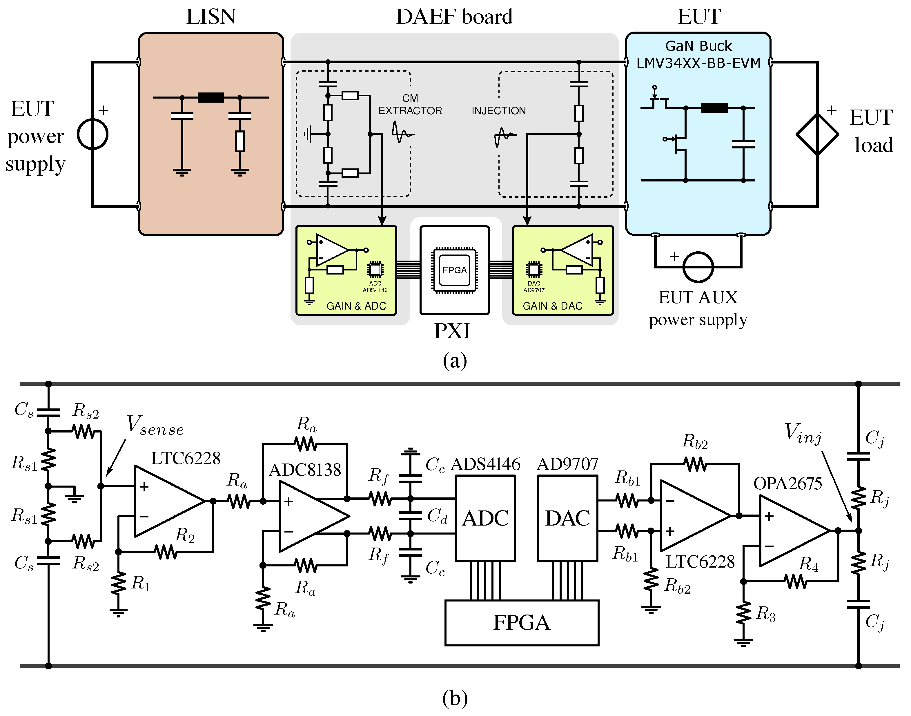
The DAEF system is composed of an FPGA combined with a fast analog-to-digital converter (ADC), a digital-to-analog converter (DAC), and their conditioning circuits (i.e., CM extractor and injection network). A more detailed block diagram showing the system is reported in Figure 3. The CM extractor is realized with two high-pass filters, designed to achieve unity gain and negligible phase shift from 150 k Hz onwards. Considering the maximum input CM voltage, the gain of the non-inverting amplifier is set to use the maximum dynamic input range of the ADC. Because of the high bandwidth of the amplifier, the feedback resistance is set to a low value in order to improve the stability of the amplifier, reducing the impact of parasitic capacitance between the non-inverting input pin and ground. The single-ended-to-differential amplifier gain is set to unity to guarantee stable performance, as suggested by the datasheet guidelines. The output of the used DAC is a dual-current output, for this reason, a transimpedance amplifier is necessary. The design of this stage is performed using the same operational amplifier of the input stage. The output voltage is then amplified by a factor of two using a high-current, high-bandwidth non-inverting amplifier. The RC injection network is used to interface the output of the amplifier to the power lines. A good coupling is needed in the frequency range of interest; however, the differential current due to the inserted impedance must be limited. For this reason, a trade-off of the capacitor value is needed. Table 2 summarizes the main active components used in the application herein, while Table 3 lists the values of the related passive components. All the circuits for noise sensing and injection are embedded within a single PCB; this is different to other solutions like, for example, Ref. [8]. The control algorithm is deployed on a Xilinx Kintex-7 325T FPGA of an NI PXIe-7862 board. The FPGA is used to synchronize all the signals with the switching period of the converter and the data exchange from ADC and to DAC. Data processing is performed in real time, such that the FPGA acquires data from the ADC and communicates the compensation signal to be injected to the DAC, synchronously with the operation of the converter. The EUT is constituted by a synchronous buck converter implemented by a Texas Instruments board [23] using GaN devices LMG341xR050 [24]. In order to normalize the power supply impedance, a line impedance stabilization network (LISN) is employed on each power line.

5. Experimental Results

5.1. Experimental Testbench

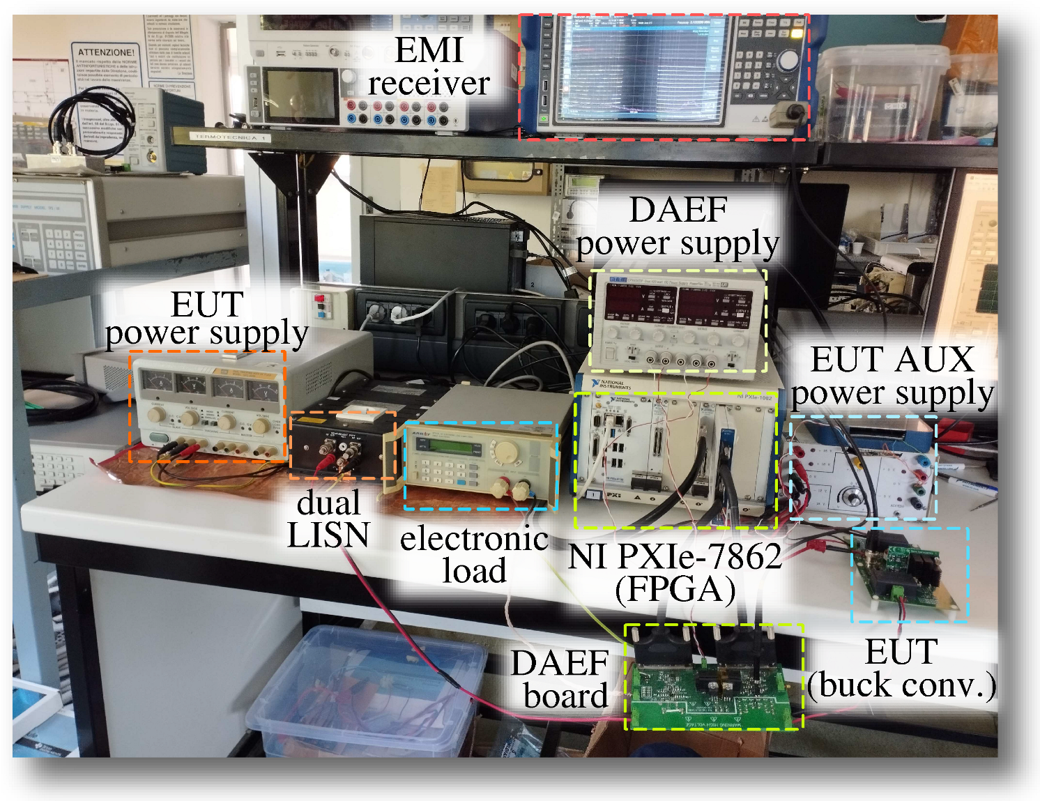
Figure 4 displays the experimental testbench, composed of the DAEF board implementing the circuit represented in Figure 3b and the EUT, constituted of a buck converter feeding an electronic load. The source of the DC supply energizing the EUT is provided by a laboratory power supply connected to the input of the EUT through an LISN. The DAEF is connected in parallel to the lines interconnecting the LISN output with the EUT. A copper plane is used as a ground reference plane and is connected to PE; low-impedance connections to this plane are ensured for the LISN, the power supply, the electronic load, and the DAEF. An EMI test receiver, R&S EPL-1000, is connected to the DAEF common-mode noise extractor using a voltage probe and a spring clip. In addition, two power supplies are employed to power the DAEF and the EUT circuits, denoted as DAEF and EUT in Figure 4, respectively. The buck converter duty cycle is controlled synchronously with the DAEF.

5.2. Experimental Measurements

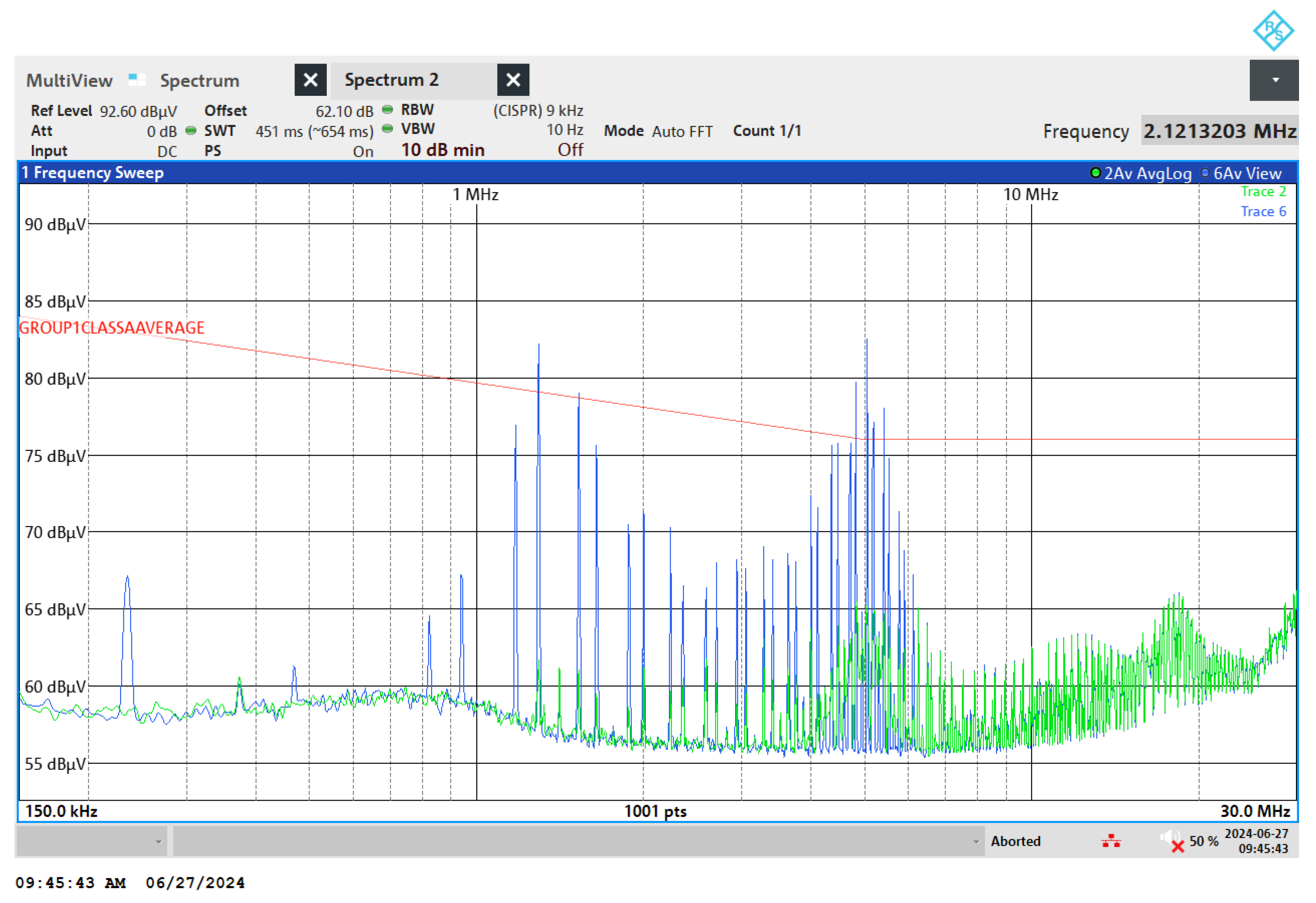
In this section, the experimental results obtained using the test setup reported in Figure 4 are shown. The noise is measured using an EMI receiver (R&S EPL1000) the measurement point is the CM extractor of the DAEF board. The EMI receiver is set with an RBW of 9 kHz and a VBW of 10 Hz . The synchronous buck converter is operated in steady state with an input voltage of 25 V and a switching frequency f s w = 119 kHz , with a duty cycle δ = 0.632 . The electronic load is set in resistance mode with R o = 7.2 Ω . The noise produced in this condition is shown in Figure 5 with the blue trace. The harmonics with higher amplitudes are present in the ranges 1 MHz 2 MHz and 4 MHz 6 MHz .
Figure 5 reports the noise before compensation and the residual noise after applying the DAEF. In order to show the DAEF effect on the CM noise, considering a possible EMC standard, the CISPR11 class-A average is referred to in the figure. The spectrum is reduced over a wide range of frequencies. Table 4 reports the attained reduction considering the largest harmonic components. Noise attenuation up to 20 dB μ V is recorded in this case. Notably, all the harmonics comply with the standard considered for demonstration after DAEF activation.
For completeness, a spectrogram showing the effect on harmonic attenuation after the activation of the DAEF is reported in Figure 6. The plot shows the intensity of the different spectral components during a time window of about 60 s .
The intensity of the harmonic components is represented by colors, the x-axis shows the frequency of the spectral components, and the y-axis represents the time, with the most recent measurements on the top part of the graph. On the bottom part of the graph, the DAEF is disabled, then the compensation algorithm is activated and the intensity of the different spectral components, starting from the most intense ones, are gradually attenuated. In the implementation, if a spectral component is smaller than a defined threshold, no adaptation is applied, which eventually leads to the steady-state operation visible in the top part of Figure 6. In this case, the threshold is set higher than the noise floor seen from the DAEF control system. The noise and the residual signal in the time domain are reported in Figure 7. Remarkably, the residual noise after compensation is significantly reduced.

6. Conclusions

This paper discusses the potential of digital active EMI filters (DAEFs) in smart power electronic systems and proposes an implementation and control algorithm of a common-mode DAEF. The proposed approach exploits transfer-function mapping and an online adaptation of the compensation signal to achieve an effective EMI attenuation. Furthermore, transfer-function characterization may potentially be exploited for anomaly detections (e.g., wearing of insulation in motors) in future applications. The developed DAEF is demonstrated using a single-board implementation integrating sensing, acquisition, and signal compensation injection, eliminating the need for additional common-mode or differential-mode passive filters. Additional functions that may be implemented by the DAEF were also envisioned considering future smart electronic power converters.

Author Contributions

Conceptualization, T.C. and D.B.; Methodology, T.C. and M.S.; Software, M.D.; Validation, M.D. and M.S.; Formal analysis, M.S.; Investigation, M.D.; Data curation, M.D.; Writing—original draft, M.D.; Writing—review & editing, T.C. and D.B.; Supervision, T.C. and D.B.; Project administration, T.C.; Funding acquisition, D.B. All authors have read and agreed to the published version of the manuscript.

Funding

This research was supported in part by the Italian Ministry of University and Research (MUR) under the National Recovery and Resilience Plan (NRRP), Mission 4 Component 2 Investment 1.3—Call for tender No. 0341 published on 15 March 2022, funded by the European Union NextGenerationEU-Project Title Network 4 Energy Sustainable Transition NEST, under Project PE0000021, Concession Decree No. 1561 of 11 October 2022 by MUR, CUP C93C22005230007.

Data Availability Statement

The original contributions presented in the study are included in the article, further inquiries can be directed to the corresponding authors.

Conflicts of Interest

The authors declare no conflicts of interest.

Abbreviations

The following abbreviations are used in this manuscript:
FFTFast Fourier transform
PEProtective earth
CMCommon mode
DMDifferential mode
ADCAnalog-to-digital converter
DACDigital-to-analog converter
EMCElectromagnetic compatibility
EMIElectromagnetic interference
AEFActive EMI filter
EUTEquipment under test
DAEFDigital active EMI filter
WBDWide-bandgap device

References

  1. Gurpinar, E.; Castellazzi, A. Single-Phase T-Type Inverter Performance Benchmark Using Si IGBTs, SiC MOSFETs, and GaN HEMTs. IEEE Trans. Power Electron. 2016, 31, 7148–7160. [Google Scholar] [CrossRef]
  2. Zhang, B.; Wang, S. A Survey of EMI Research in Power Electronics Systems with Wide-Bandgap Semiconductor Devices. IEEE J. Emerg. Sel. Top. Power Electron. 2020, 8, 626–643. [Google Scholar] [CrossRef]
  3. Dey, S.; Mallik, A.; Mishra, S. A Mathematical Design Approach to Volumetric Optimization of EMI Filter and Modeling of CM Noise Sources in a Three-Phase PFC. IEEE Trans. Power Electron. 2022, 37, 462–472. [Google Scholar] [CrossRef]
  4. Son, Y.C.; Sul, S.K. Generalization of active filters for EMI reduction and harmonics compensation. IEEE Trans. Ind. Appl. 2006, 42, 545–551. [Google Scholar] [CrossRef]
  5. Chen, W.; Yang, X.; Wang, Z. Analysis of Insertion Loss and Impedance Compatibility of Hybrid EMI Filter Based on Equivalent Circuit Model. IEEE Trans. Ind. Electron. 2007, 54, 2057–2064. [Google Scholar] [CrossRef]
  6. Jiang, S.; Liu, Y.; Liang, W.; Peng, J.; Jiang, H. Active EMI Filter Design with a Modified LCL-LC Filter for Single-Phase Grid-Connected Inverter in Vehicle-to-Grid Application. IEEE Trans. Veh. Technol. 2019, 68, 10639–10650. [Google Scholar] [CrossRef]
  7. Narayanasamy, B.; Luo, F.; Chu, Y. Modeling and Stability Analysis of Voltage Sensing based Differential Mode Active EMI Filters for AC-DC Power Converters. In Proceedings of the 2018 IEEE Symposium on Electromagnetic Compatibility, Signal Integrity and Power Integrity (EMC, SI & PI), Long Beach, CA, USA, 30 July–3 August 2018; pp. 322–328. [Google Scholar] [CrossRef]
  8. Bendicks, A.; Gerten, M.; Frei, S. Active Cancellation of Periodic CM EMI at the Input of a Motor Inverter by Injecting Synthesized and Synchronized Signals (S3-AEF). IEEE Trans. Power Electron. 2022, 37, 11951–11961. [Google Scholar] [CrossRef]
  9. Hamza, D.; Pahlevaninezhad, M.; Jain, P.K. Implementation of a Novel Digital Active EMI Technique in a DSP-Based DC–DC Digital Controller Used in Electric Vehicle (EV). IEEE Trans. Power Electron. 2013, 28, 3126–3137. [Google Scholar] [CrossRef]
  10. Ji, J.; Chen, W.; Yang, X. Arc welding inverter with embedded Digital Active EMI controller. In Proceedings of the 2016 IEEE Applied Power Electronics Conference and Exposition (APEC), Long Beach, CA, USA, 20–24 March 2016; pp. 493–498. [Google Scholar] [CrossRef]
  11. Liserre, M.; Beiranvand, H.; Leng, Y.; Zhu, R.; Hoeher, P.A. Overview of Talkative Power Conversion Technologies. IEEE Open J. Power Electron. 2023, 4, 67–80. [Google Scholar] [CrossRef]
  12. Leng, Y.; Zhu, R.; Liserre, M.; Hoeher, P.A. Variable Zero-Vector-Width-Based Three-Phase DC/AC Talkative Power Conversion. IEEE J. Emerg. Sel. Top. Power Electron. 2024, 12, 3402–3414. [Google Scholar] [CrossRef]
  13. Bendicks, A.; Dörlemann, T.; Frei, S.; Hees, N.; Wiegand, M. Active EMI Reduction of Stationary Clocked Systems by Adapted Harmonics Cancellation. IEEE Trans. Electromagn. Compat. 2019, 61, 998–1006. [Google Scholar] [CrossRef]
  14. TPSF12C1-Q1 Standalone; Active, EMI Filter for Common-Mode Noise Mitigation in Single-Phase, AC, Automotive Power Systems. Mouser Electronics: Mansfield, TX, USA, 2023.
  15. Zhou, Y.; Chen, W.; Yang, X.; Zhang, R.; Yan, R.; Liu, J.; Wang, H. A New Integrated Active EMI Filter Topology with Both CM Noise and DM Noise Attenuation. IEEE Trans. Power Electron. 2022, 37, 5466–5478. [Google Scholar] [CrossRef]
  16. Han, Y.; Wu, Z.; Wu, D. Hybrid Common-mode EMI Filter Design for Electric Vehicle Traction Inverters. Chin. J. Electr. Eng. 2022, 8, 52–60. [Google Scholar] [CrossRef]
  17. Douzi, S.; Tlig, M.; Slama, J.B.H.; Kadi, M. Simulation of conducted EMI in SiC MOSFET buck converters before and after aging. In Proceedings of the 2016 7th International Conference on Sciences of Electronics, Technologies of Information and Telecommunications (SETIT), Hammamet, Tunisia, 18–20 December 2016; pp. 171–176. [Google Scholar] [CrossRef]
  18. Mannan, T.I.; Amin, A.; Choi, S. Investigation of SiC MOSFET Aging Effects on Common-Mode EMI Emissions. In Proceedings of the 2023 IEEE Electric Ship Technologies Symposium (ESTS), Alexandria, VA, USA, 1–4 August 2023; pp. 477–483. [Google Scholar] [CrossRef]
  19. Douzi, S.; Tlig, M.; Slama, J.B.H. Experimental investigation on the evolution of a conducted-EMI buck converter after thermal aging tests of the MOSFET. Microelectron. Reliab. 2015, 55, 1391–1394. [Google Scholar] [CrossRef]
  20. Narayanasamy, B.; Luo, F. A Survey of Active EMI Filters for Conducted EMI Noise Reduction in Power Electronic Converters. IEEE Trans. Electromagn. Compat. 2019, 61, 2040–2049. [Google Scholar] [CrossRef]
  21. Jiang, L.; Wang, F.; Szolusha, K.; Mathews, K. A Practical Method for Separating Common-Mode and Differential-Mode Emissions in Conducted Emissions Testing. Analog. Dialogue 2021, 55, 1–4. [Google Scholar]
  22. Biancacci, N. FFT corrections for tune measurements. In Proceedings of the Optics Workshop, OMCM, Geneva, Switzerland, 20–22 June 2011. [Google Scholar]
  23. Texas Instruments Incorporated. Using the LMG3410-HB-EVM Half-Bridge and LMG34XX-BB-EVM Breakout Board EVM. In General TI High Voltage Evaluation User Safety Guidelines; Texas Instruments Incorporated: Dallas, TX, USA, 2016. [Google Scholar]
  24. Texas Instruments Incorporated. LMG341xR050 600-V 50-mΩ Integrated GaN Fet Power Stage with Overcurrent Protection; Texas Instruments Incorporated: Dallas, TX, USA, 2020. [Google Scholar]
Figure 1. Architecture of a DAEF connected at the interface between a noise source, typically referred to as EUT, and the mains.
Electronics 13 03889 g001
Figure 2. Flowchart of the proposed adaptive control algorithm for the DAEF, comprising the preliminary characterization of the transfer function between voltage injection and sensing [i.e., H ( f ) ].
Electronics 13 03889 g002
Figure 3. Details of DAEF connected to the considered test setup: (a) main blocks of test setup organization; (b) principle diagram of the DAEF circuit.
Electronics 13 03889 g003
Figure 4. Experimental testbench.
Electronics 13 03889 g004
Figure 5. Comparison between the measured noise with disabled DAEF (blue trace) and after DAEF activation (green trace).
Electronics 13 03889 g005
Figure 6. Spectrogram of the measured noise after the activation of the DAEF.
Electronics 13 03889 g006
Figure 7. Voltage waveforms of the measured EUT noise: (a) EUT noise with DAEF disabled; (b) residual noise after DAEF activation.
Electronics 13 03889 g007
Table 1. Typical performances and features of representative EMI filter solutions.
Filter TypeMax AttenuationFeatures
AEF  [15] 30 dB @ 150 k Hz CM/DM reduction
Hybrid [16] 26 dB @ 4.7 M Hz Broadband suppression
DAEF  [8] 65 dB @ 400 k Hz Flexibility, strong reduction
Table 2. Main components of the DAEF circuit (see Figure 3).
ComponentFunction
ADS4146Fast ADC used to sample the noise; 160 MS/s with 14-bit resolution.
AD9707Fast DAC with dual-current output; 175 MS/s with 14-bit resolution.
LTC6228Operational amplifier used to amplify the common mode.
AD8138Single-ended-to-differential driver.
OPA2675High-current-operation amplifier used to drive the injection circuit.
Table 3. Values of the components shown in Figure 3.
SymbolValueSymbolValueSymbolValue
R S 1 1.2 k Ω R 2 1 k Ω R 3 510 Ω
C s 5.1 n F R a 510 Ω R 4 510 Ω
R s 2 510 Ω R b 1 510 Ω R j 150 Ω
R 1 510 Ω R b 2 1 k Ω C j 6.8 n F
Table 4. Main noise harmonics and related attenuation after DAEF activation.
Freq. (MHz) Δ noise ( dB μ V ) Freq. (MHz) Δ noise ( dB μ V ) Freq. (MHz) Δ noise ( dB μ V )
1.171901161.178127191.28916819
1.296017201.527364181.53547813
1.644966164.113723124.36060114
4.721303134.822430155.05795818
Disclaimer/Publisher’s Note: The statements, opinions and data contained in all publications are solely those of the individual author(s) and contributor(s) and not of MDPI and/or the editor(s). MDPI and/or the editor(s) disclaim responsibility for any injury to people or property resulting from any ideas, methods, instructions or products referred to in the content.