Article

A Frequency-Reconfigurable Dual-Band RF Crossover Based on Coupled Lines and Open Stubs

by
Abdullah J. Alazemi
* and
Danah H. Almatar
Department of Electrical Engineering, Faculty of Engineering and Petroleum, Kuwait University, Safat, Kuwait City 13060, Kuwait
*
Author to whom correspondence should be addressed.
Electronics 2024, 13(13), 2641; https://doi.org/10.3390/electronics13132641
Submission received: 7 June 2024 / Revised: 29 June 2024 / Accepted: 2 July 2024 / Published: 5 July 2024
(This article belongs to the Special Issue Microwave Devices: Analysis, Design, and Application)

Abstract

:
This paper presents a frequency-reconfigurable dual-band radio frequency (RF) crossover based on quarter-wavelength coupled lines (CLs) and open stubs. Initially, an even–odd-mode analysis was conducted for the design, and closed-form equations were found. Then an advanced design system (ADS) was utilized to support and further optimize the theoretical analysis. Afterwards, high-frequency simulation software (HFSS) was used to simulate the proposed design. The proposed device is printed on a 1.524 mm RO4003C printed-circuit board ( ε r = 3.55 ) . The frequency tunability is achieved by employing two varactor diodes connected to the open stubs. When the biasing voltage is altered, the capacitance of the SMV1405 varactor can change from 2.67 pF to 0.63 pF. Accordingly, the two operating frequencies can be continuously tuned from 2.06 GHz to 2.40 GHz and from 5.44 GHz to 5.84 GHz. For the low-frequency range, return loss and isolation are above 15 dB, and the insertion loss is less than 1.1 dB. As for the high-frequency range, the return loss is greater than 20 dB, the isolation is better than 15 dB, and the insertion loss is lower than 1.6 dB. The measurement results agreed well with the simulation results, and the crossover overall size is 45.5 mm × 29.4 mm. The proposed device can be utilized for various application areas, such as 5G smartphone applications and satellite communication.

1. Introduction

A radio frequency (RF) crossover is a passive microwave device that consists of four ports: two input ports and two output ports. Its main purpose is to ensure the passage of two signals traveling across each other simultaneously with minimal interference. In this device, one signal travels from port 1 to port 3, and the second signal travels from port 2 to port 4. Also, all of the crossover ports must be matched. This microwave device is of great importance in beamforming networks (BFNs) such as butler matrices (BMs). BMs play an essential role in feeding networks of antenna arrays. Thus, it has the ability to control the steering of the main beam, can realize multi-beam response, or can provide wide coverage with high gain if properly designed [1]. BMs conventionally consist of couplers, crossovers, and phase shifters. Accordingly, the characteristics of the BM will be the same as the characteristics of its components. As a result, many investigations were conducted to enhance the performance of BMs and realize demanded features such as wideband response [2,3], multi-band response [4], reconfigurable response [5], or reaching a compact design [6,7]. Therefore, crossovers have been widely researched and designed using various techniques. Starting from a non-planar model using airbridges to prevent metallic connectivity between the four ports, we achieve two separate paths [8]. Another design was presented using a multi-layer structure where there exist two paths: one regular path using a transmission line (TL), and the other is physically disconnected but electrically connected by utilizing the additional PCB layer [9]. Capacitors and inductors can be employed to fulfill a compact crossover [10]. Also, a multi-section branch-line coupler (BLC) can realize crossover performance [11]. Negative-refractive-index transmission line (NRI-TL) metamaterial lines were used to design a crossover [12]. The design was accomplished by loading the TLs of three BLCs with shunt inductors and series capacitors. Moreover, filtering crossover was achieved using a ring resonator [13]. Microstrip square, circular, and hexagonal patch crossovers were investigated [14]. Also, a square patch was used to achieve a crossover design; however, in this design, the implementation of different slot shapes on the patch was researched [15]. Another approach to realizing a crossover is by utilizing CLs. Usually, crossovers based on CLs lead to a compact design [16].
Along with the rapid and continuous advancement of technology, the development of microwave devices capable of operating at different resonant frequencies [17,18,19,20,21,22,23,24] or multi-tasking using the same device [25,26,27,28,29,30,31,32,33,34,35] became a necessity. Crossover with dual-band response was achieved by increasing the length of the vertical TLs of a branch-line crossover (BLCO) to double the length of the horizontal TLs [20]. Also, the replacement of the horizontal TLs of a BLCO by a T-network can accomplish a dual-band crossover [21]. Cascading a dual-band coupler can lead to a dual-band crossover [22]. Furthermore, CLs were utilized to realize the dual-band response [23,24]. All of the aforementioned dual-band designs can only operate at two fixed frequencies.
The following crossover designs resonate at a single frequency but with the ability to tune that operating frequency. One way of achieving frequency tuneability is by employing rectangular dielectric channels (RDCs) in a BLCO [25]. Then, by filling the RDCs with air or dielectric materials, the frequency will change as the permittivity changes. Another way of realizing tunability is by employing varactor diodes that can give different capacitances based on the applied biasing voltage. Substrate integrated waveguide (SIW) evanescent-mode cavity resonators along with four sets of varactors were used to achieve a frequency-reconfigurable crossover [26]. Two CLs, two constant capacitors, and one varactor diode have been incorporated to alter a crossover frequency [27]. Using the same design, instead of one, three varactor diodes were implemented instead of one [28].
As per the conducted investigation, there exists no frequency-reconfigurable crossover operating at two frequencies. Therefore, a dual-band crossover with tuneable frequencies has been analyzed, designed, simulated, fabricated, and measured. Some considerations were followed while conducting the design, such as achieving a planar design that can be easily integrated with other microwave devices. The size of the design should be reasonable. The complexity of the design shall be avoided to simplify the fabrication process and decrease the cost. Using few switching elements since its increase will consequently lead to more soldering required and more resistance. Thus, insertion loss, isolation loss, and return loss can be negatively affected. Also, it will increase the number of biasing circuits needed.
The proposed design is accomplished by using four CLs, two open stubs, and two varactor diodes while maintaining the symmetry of the design to reach closed-form equations from the even–odd-mode analysis. The low frequency can be changed from 2.06 GHz to 2.40 GHz with a tuning range of 15.3%. The high frequency can be altered from 5.44 GHz to 5.84 GHz, and the tuning range is 7.1%. The proposed crossover can be used for WiMAX (2.3 GHz and 5.8 GHz) and IEEE 802.11 WLAN (2.4 GHz and 5.725 to 5.82 GHz) applications.
In the next section, Section 2, the theoretical analysis of the proposed design, basically the even–odd-mode analysis, crossover conventional specifications, CL constraints, and advanced design system (ADS) [36] results are presented. Section 3 is about simulating the design using high-frequency simulation software (HFSS) [37], where an insight into the covered frequencies and S-parameters of the design can be found. Then, Section 4 is regarding implementation and measurement, where the crossover fabrication, S-parameter measurements, results discussion, and comparison with the aforementioned published designs are stated. Lastly, Section 5 is the conclusion of the proposed design.

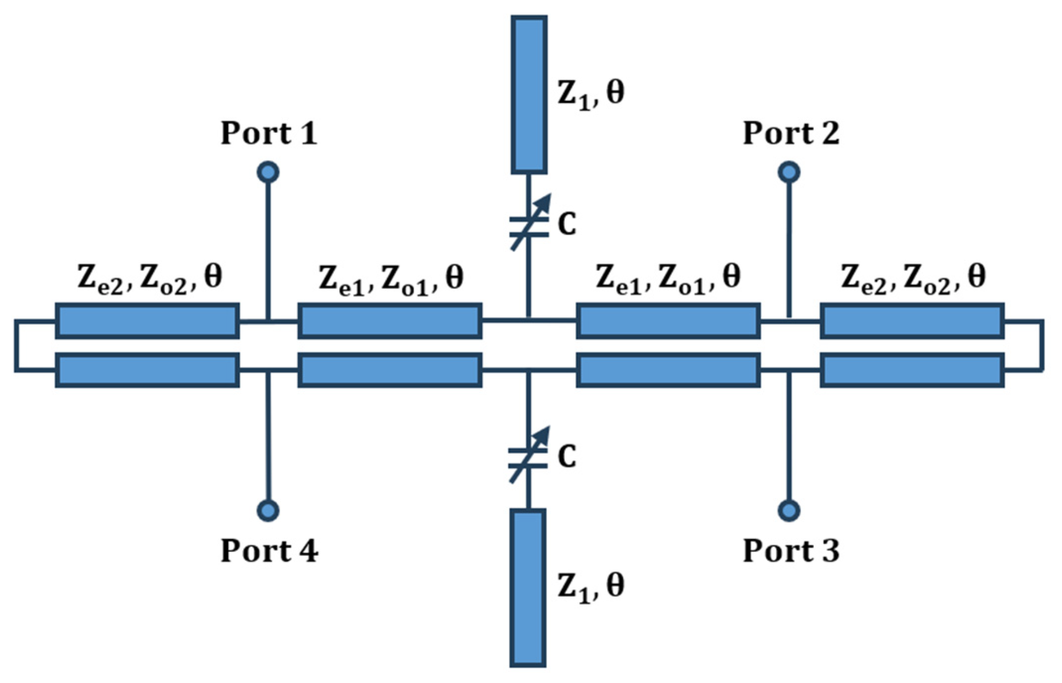
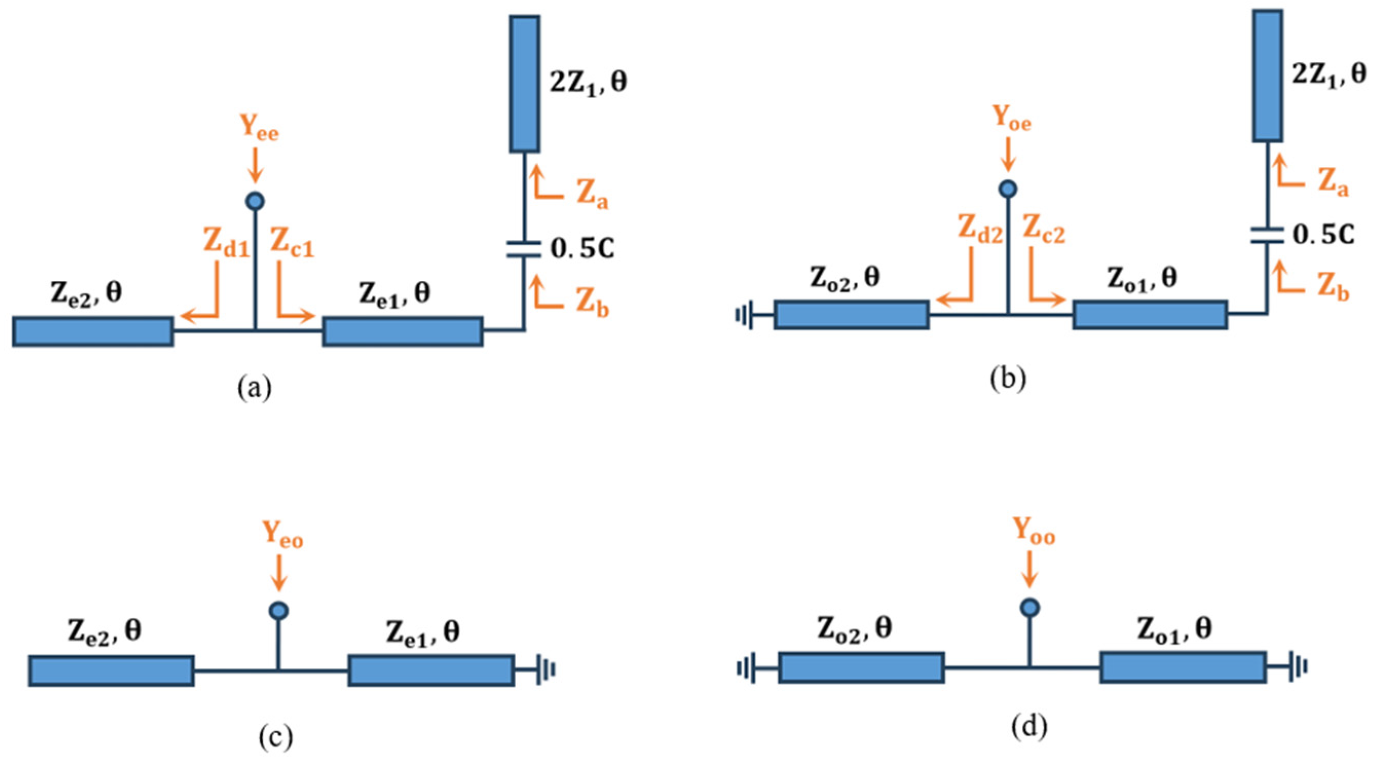
2. Theoretical Analysis

The circuit schematic of the proposed dual-band frequency-reconfigurable crossover is shown in Figure 1. Four quarter-wavelength CLs are utilized, along with two open 90° stubs. There are two sets of CLs regarding the even and odd impedances ( Z e 1 , Z o 1 ) and ( Z e 2 , Z o 2 ). Whereas the stubs have an impedance of Z 1 and each stub is connected through a varactor diode, so two varactor diodes are used.
The design is symmetric along both the horizontal and vertical axes to ensure finding closed-form equations and simplify the design process. Consequently, even–odd-mode analysis is carried out [38], and Figure 2 shows the equivalent even–even, odd–even, even–odd, and odd–odd circuits.
The equations corresponding to these circuits are as follows:
Z a = j 2 Z 1 tan θ
Z b = j 2 Z 1 tan θ + 1 0.5 ω C  
Z c 1 = Z e 1 Z b + jZ e 1 tan θ Z e 1 + jZ b tan θ
Z d 1 = j Z e 2 tan θ
The even–even admittance:
Y ee = 1 Z c 1 + 1 Z d 1 = j tan θ Z e 2 1 Z e 1 0.5 ω CZ e 1 tan θ + Z 1 ω C tan θ + tan θ 2 Z 1 ω C + tan θ 0.5 ω CZ e 1 tan θ 2
Z c 2 = Z o 1 Z b + jZ o 1 tan θ Z o 1 + jZ b tan θ  
Z d 2 = jZ o 2 tan θ  
The odd–even admittance:
Y oe = 1 Z c 2 + 1 Z d 2 = j cot θ Z o 2 + 1 Z o 1 0.5 ω CZ o 1 tan θ + Z 1 ω C tan θ + tan θ 2 Z 1 ω C + tan θ 0.5 ω CZ o 1 tan θ 2  
The even–odd admittance:
Y eo = j tan θ Z e 2 cot θ Z e 1
The odd–odd admittance:
Y oo = j cot θ Z o 2 + cot θ Z o 1
To realize a crossover design, the following criteria should be met:
S 11 = S 22 = S 33 = S 44 = 0  
S 21 = S 41 = S 32 = S 43 = 0
S 31 = S 42 = 1
where S 11 is the return loss, S 31 is the insertion loss, and S 21 and S 41 are isolation S-parameters. Since the crossover is a passive microwave device, it means that its scattering matrix is reciprocal:
S = | S 11 | | S 12 | | S 13 | | S 14 | | S 21 | | S 22 | | S 31 | | S 32 | | S 41 | | S 42 | | S 23 | | S 24 | | S 33 | | S 34 | | S 43 | | S 44 | = 0 0 1 0 0 0 1 0 0 1 0 1 0 0 0 0
The S-parameters can be calculated using
S 11 = Γ ee + Γ eo + Γ oe + Γ oo 4
S 21 = Γ ee Γ eo + Γ oe Γ oo 4  
S 31 = Γ ee Γ eo Γ oe + Γ oo 4
S 41 = Γ ee + Γ eo Γ oe Γ oo 4
where the input reflection coefficients can be calculated using
Γ ee , eo , oe , oo = 1 Z o Y ee , eo , oe , oo 1 + Z o Y ee , eo , oe , oo
Then, by substituting (14)–(18) in (11)–(13), the following equations are found:
Γ ee = Γ oo = Γ eo = Γ oe
Y ee = Y oo  
Y eo = Y oe
Z o 2   Y ee   Y eo = 1  
Also, the tuning range [39] can be calculated using
Tuning   Range   % = f High f Low f High   f Low × 100 %
  • f High : the highest resonant frequency that can be obtained in a band from tuning.
  • f Low : the lowest resonant frequency that can be obtained in a band from tuning.
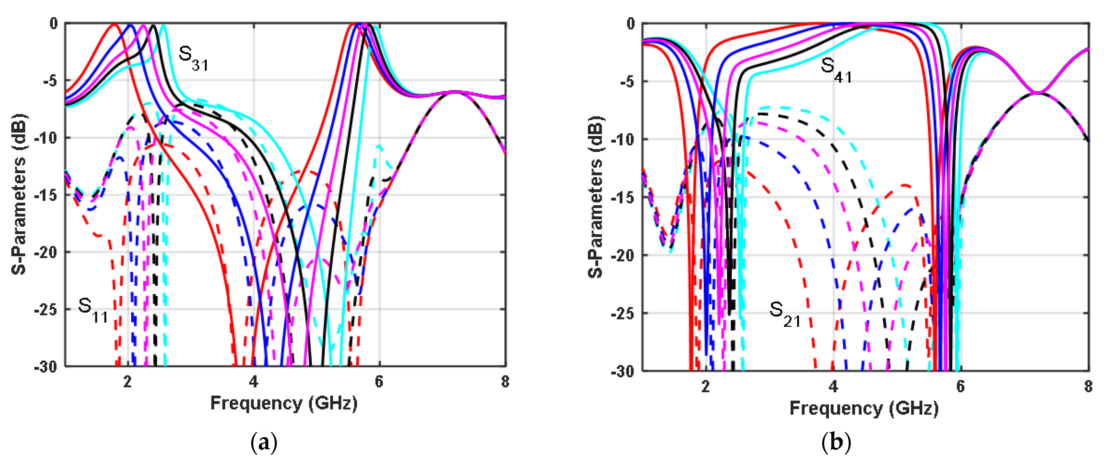
In addition, there are constraints regarding any CL to enable or facilitate its fabrication process. The even impedance must be greater than the odd impedance. Otherwise, the gap between the two TLs will be big, leading to uncoupling. Another condition that must be met is that the even impedance to odd impedance ratio should not be very high. If so, the gap between the two TLs will be very small, making the fabrication process a hard or impossible task to accomplish. Also, it may lead to high coupling, which can ruin the design.
While keeping in mind these considerations, the proposed crossover can be designed to operate in different frequency bands based on the selection of the varactor diode and the parameters of the CLs and open stubs. Also, the change in capacitance affects the quality factor, which accordingly will modify the BW. Therefore, the circuit parameters were selected to work on frequencies that realize the previously mentioned applications, and these parameters are shown in Table 1.
Afterwards, MATLAB [40] was used to ensure the correction of the previously stated equations. Additionally, ADS was utilized to verify the validation of the design and to further aid in the optimization process. Figure 3 shows an illustration of the theoretical S-parameters of the proposed design and the change in frequencies that result from changing the capacitance of the varactor diodes. It can be seen that the increase in capacitance leads to a decrease in operating frequencies.

3. Simulation

To simulate the proposed design, the physical dimensions of the ports, CLs, and open stubs are required. These dimensions were obtained by utilizing LineCalc, which is a tool provided in ADS. The electrical parameters of a CL are the even mode impedance, odd mode impedance, frequency, and electrical length; they were converted to width, length, and separation between the two lines. As for a TL, the impedance, frequency, and electrical length are used to find the physical width and length. Then HFSS was used to simulate and further optimize the design, especially because the position of the varactor diode along the open stubs affects the S-parameters, resonant frequencies, and tuning range proportion between the two bands [39]. It can be noticed that there is a considerable difference between Z e 1 and Z o 1 , and as previously mentioned, this can lead to high coupling, which can negatively affect the results. This was proven when the design was simulated. Thus, the patterned ground technique [41] was employed, and two slots were etched at the ground plane to reduce the coupling effect. After that, the design was simulated, and Figure 4 shows the S-parameters of the proposed design.
When the capacitance of the varactor diodes was set to 2.67 pF, the dual-band frequencies obtained were 2.09 GHz and 5.44 GHz. Then, when the capacitance was decreased, the operating frequencies increased. Until reaching 0.63 pF, the frequencies were continuously tuned until reaching 2.49 GHz and 5.80 GHz. The tuning range was calculated using Equation (23). For the lower band, the tuning range is 17.5%. Whilst for the higher band, the tuning range is 6.4%. In both bands along the whole tuning range, the insertion loss | S 31 | dB   is less than 1.4 dB. For the lower band, | S 11 | dB is above 12 dB, | S 21 | dB is greater than 16 dB, and | S 41 | dB is better than 13 dB. Going to the higher band, | S 11 | dB is higher than 24 dB, | S 21 | dB is above 13 dB, and | S 41 | dB is more than 20 dB.

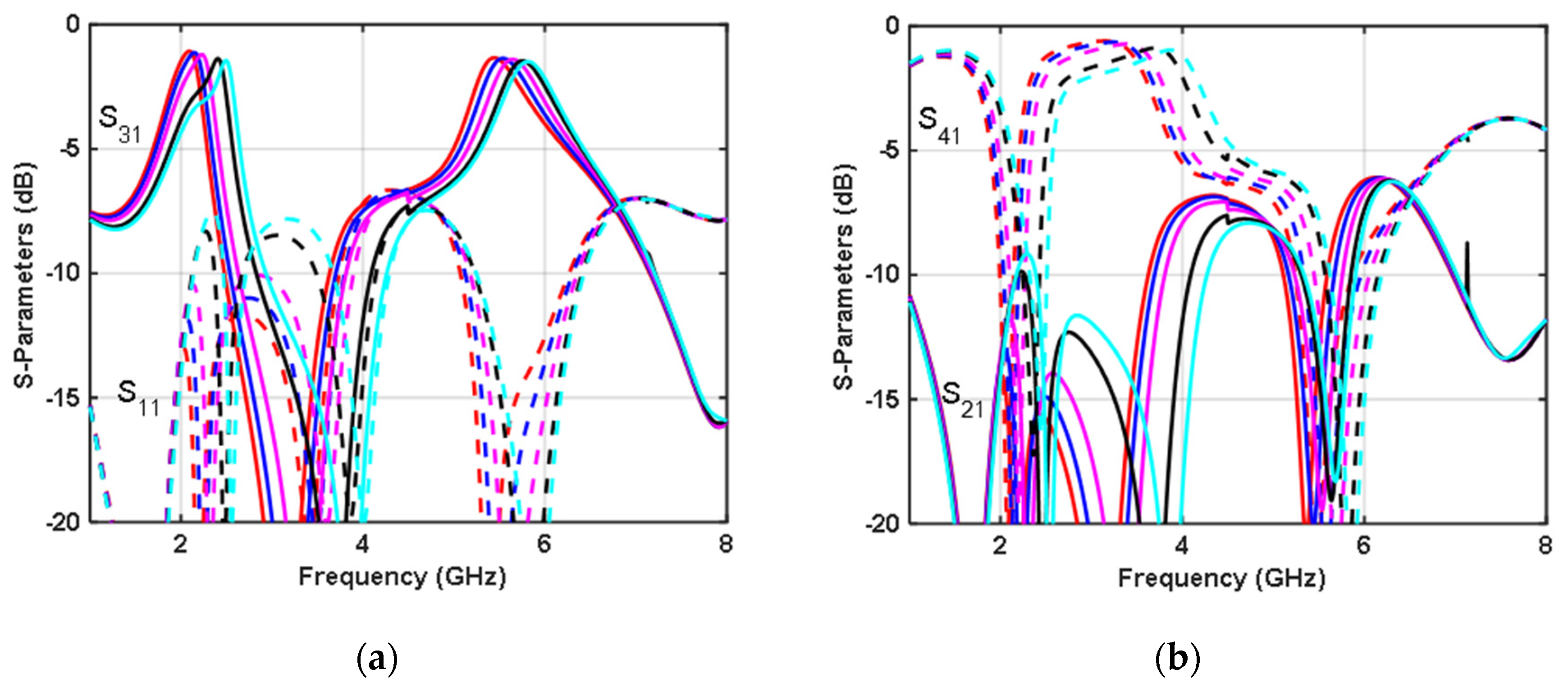
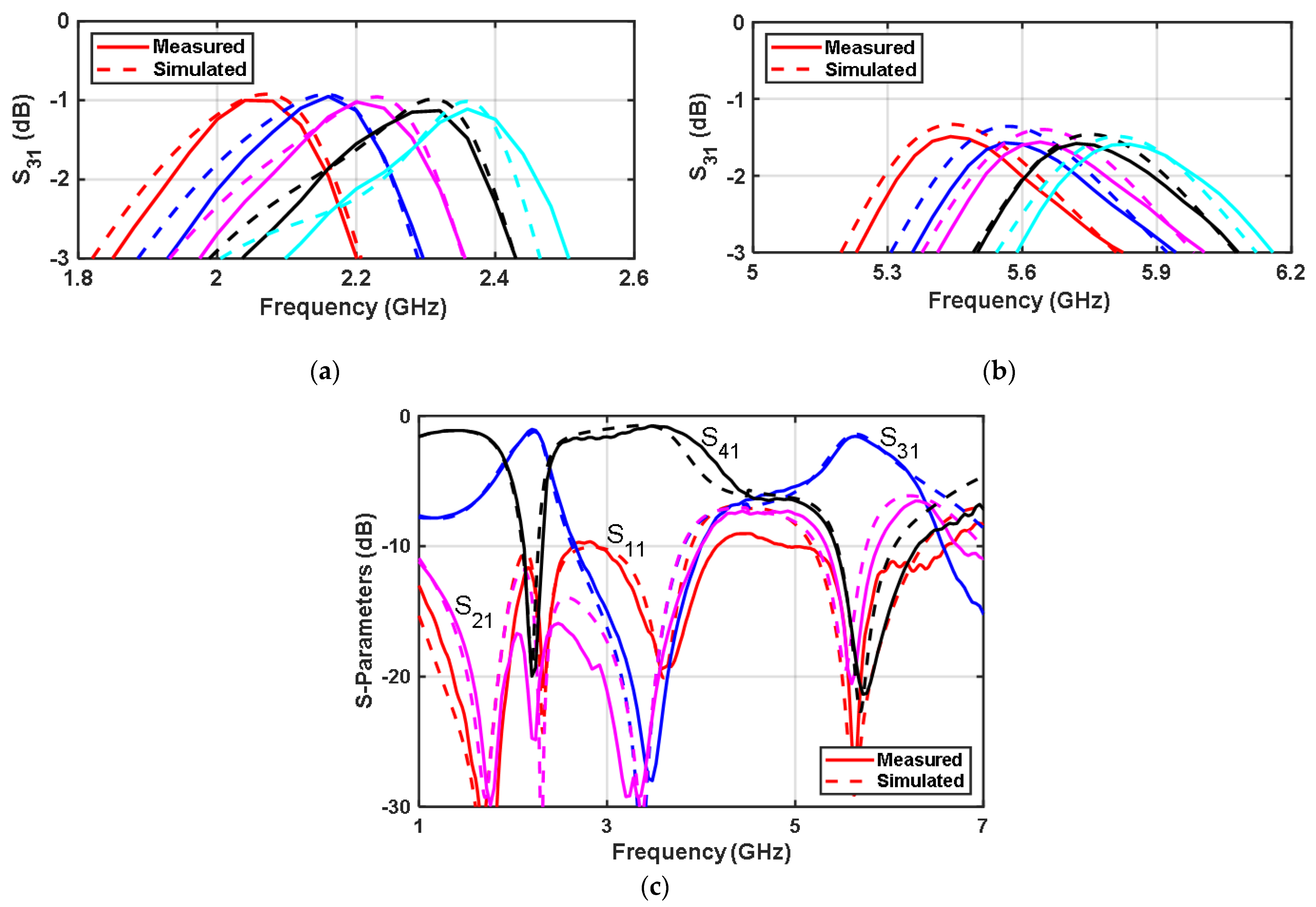
4. Implementation and Measurement

The proposed dual-band frequency-reconfigurable crossover was fabricated using printed circuit board (PCB) technology. The design was accomplished by utilizing a RO4003C substrate that has a dielectric constant ( ε r ) of 3.55; its loss tangent tan δ is 0.0027; and the thickness ( h ) selected is 1.524 mm. As for the two varactor diodes employed in the design, SMV1405 was chosen. The varactor diode’s equivalent circuit is shown in Figure 5. This diode has an inductance (L) of 0.7 nH, a resistance (R) of 0.8 Ω, and its capacitance (C) can be altered from 2.67 pF to 0.63 pF. The 2.67 pF capacitance can be achieved as the DC biasing voltage is 0 V, and as the voltage increases, the capacitance decreases. Once the biasing voltage reaches 30 V, the capacitance becomes 0.63 pF. The dimensions used in the fabrication process of the proposed crossover are displayed in Table 2. Figure 6 shows the proposed design circuit layout along with the fabricated prototype. The size of the proposed crossover (without considering the port lines and biasing circuits) is 45.5 mm × 29.4 mm.
Measurements of the fabricated dual-band frequency-reconfigurable crossover were conducted via a network analyzer. Figure 7 shows the S-parameters ( | S 11 | dB ,   | S 21 | dB ,   | S 31 | dB ,   and   | S 41 | dB ) and their variation along the alternation of the varactor diode’s capacitance.
Table 3 and Table 4 show a summary of the capacitance, operating frequencies, and obtained S-parameters at the low-frequency band and at the high-frequency band, respectively. The capacitance of the two varactor diodes is changed by altering the biasing voltage from 0 V, which gives 2.67 pF, to 30 V, which corresponds to 0.63 pF.
The measurement of the fabricated dual-band frequency-reconfigurable crossover showed tunable frequency bands starting from 2.06 GHz to 2.40 GHz and from 5.44 GHz to 5.84 GHz. As for the return loss of the proposed design, it shows better performance in the high band compared to the lower band. | S 11 | dB was found to be greater than 15 dB for the lower band and more than 20 dB for the higher band. In contrast, the insertion loss was better at the lower band. | S 31 | dB was below 1.12 dB at the lower band, while it reached 1.6 dB at the higher band. In both cases, the isolation was above 15 dB. Regarding the tuning range for both the lower and higher bands, it has been calculated using Equation (23) and found to be 15.3% and 7.1%, respectively.
The overall performance of the fabricated prototype is in agreement with what was anticipated from the theoretical analysis and HFSS simulation. Also, the measurement results are approximately the same as those obtained from the simulation. Figure 8 shows a comparison between the S-parameters found from simulation and those obtained from measuring the fabricated prototype for five different capacitance values. The small discrepancies between the results can be due to fabrication and measurement errors, material loss, and the soldering of the varactor diodes, which can lead to additional losses.
Table 5 shows a comparison between the aforementioned published designs and the proposed dual-band frequency-reconfigurable crossover. The table compares insertion loss, return loss, isolation, covered frequency bands, tuning range, size, and the ability to resonate at single or dual frequencies.
It can be noted that [25,26,27,28] presented a tunable crossover design, but it is valid for only a single frequency. While in [22,23,24], their designs show a dual-band response achieved using CLs, the two frequencies are fixed. Accordingly, the only design that can realize both frequency reconfigurability and dual-band response is the proposed design.

5. Conclusions

In this paper, a planar crossover based on CLs and open-ended stubs has been presented. It introduced a crossover design that combined two desired aspects that had not been previously recorded. These two aspects are the dual-band response and the continued tunability of the two frequency bands. For the presented crossover, even–odd analysis, optimization of circuit parameters, simulation, fabrication, and measurements were conducted. As to the fabrication process, RO4003C ( ε r = 3.55 ) with a height of 1.524 mm was used for manufacturing the crossover using printed circuit board (PCB) technology. Eventually, a crossover capable of sweeping the two operating frequencies from 2.06 GHz to 2.40 GHz and from 5.44 GHz to 5.84 GHz was realized. This was accomplished through the employment of four CLs and two open-ended stubs connected through two SMV1405 varactor diodes. The change in the applied biasing voltage from 0 V to 30 V led to an alteration of the varactor diodes’ capacitance from 2.67 pF to 0.63 pF. Consequently, tuning ranges of 15.3% and 7.1% for the low- and high-frequency bands, respectively, were attained. Also, the patterned ground technique was employed in the design to reduce the coupling effect. As a result, good performance in terms of insertion loss, return loss, isolation, rejection between the two frequency bands, frequency ratio, and size were demonstrated. In addition, the results obtained from both the simulation and measurements showed good agreement. Also, by changing the design parameters, the proposed crossover can operate at different frequencies to satisfy variant applications. As to the fabricated crossover, it can be used for WiMAX (2.3 GHz and 5.8 GHz) and IEEE 802.11 WLAN (2.4 GHz and 5.725 to 5.82 GHz) applications. Also, further work can be performed to enhance the presented design, such as using folded lines to reduce the crossover size, selecting a dielectric substrate with better specifications to reduce losses, and employing MEMS instead of varactor diodes.

Author Contributions

Conceptualization, A.J.A.; methodology, D.H.A.; formal analysis, D.H.A.; investigation, D.H.A.; resources, A.J.A.; data curation, D.H.A.; writing—original draft preparation, D.H.A.; writing—review and editing, A.J.A.; supervision, A.J.A.; project administration, A.J.A. All authors have read and agreed to the published version of the manuscript.

Funding

The research received no external funding.

Data Availability Statement

Data is contained within the article.

Conflicts of Interest

The authors declare that they have no known competing financial interests or personal relationships that could have appeared to influence the work reported in this paper.

References

  1. Vallappil, A.K.; Rahim, M.K.A.; Khawaja, B.A.; Murad, N.A.; Mustapha, M.G. Butler Matrix Based Beamforming Networks for Phased Array Antenna Systems: A Comprehensive Review and Future Directions for 5G Applications. IEEE Access 2020, 9, 3970–3987. [Google Scholar] [CrossRef]
  2. Nachouane, H.; Najid, A.; Tribak, A.; Riouch, F. Broadband 4x4 Butler Matrix Using Wideband 90° hybrid Couplers and Crossovers for Beamforming Networks. In Proceedings of the 2014 International Conference on Multimedia Computing and Systems (ICMCS), Marrakech, Morocco, 14–16 April 2014; pp. 1444–1448. [Google Scholar]
  3. Ihlou, S.; Tizyi, H.; El Abbassi, A. Beamforming Networks Using a Broadband 4x4 Butler Matrix with Wideband Couplers and Crossovers. In Proceedings of the 2nd International Conference on Big Data, Modelling and Machine Learning, Kenitra, Morocco, 15–16 July 2021; pp. 255–259. [Google Scholar]
  4. Sivasundarapandian, S. Performance analysis of multi-band multiple beamforming butler matrix for smart antenna systems. In Proceedings of the 2015 International Conference on Robotics, Automation, Control and Embedded Systems (RACE), Chennai, India, 18–20 February 2015; pp. 1–5. [Google Scholar]
  5. Tork, A.; Natarajan, A. Reconfigurable X-Band 4×4 Butler array in 32nm CMOS SOI for angle-reject arrays. In Proceedings of the 2016 IEEE/MTT-S International Microwave Symposium (IMS), San Francisco, CA, USA, 22–27 May 2016; pp. 1–4. [Google Scholar]
  6. Heydarli, G.; Palandöken, M. A Compact Crossover Design for Butler Matrix Feeding Network in 5G Sub 6 GHz Wireless Applications. Eur. J. Sci. Technol. 2022, 39, 51–54. [Google Scholar] [CrossRef]
  7. Heba, H.; Hamza, I.; Pistono, E.; Darine, K.; Florence, P.; Abouchahine, S.; Ferrari, P. Miniaturized branch-line coupler based on slow-wave microstrip lines. Int. J. Microw. Wirel. Technol. 2018, 10, 1103–1106. [Google Scholar] [CrossRef]
  8. Horng, T.-S. A rigorous study of microstrip crossovers and their possible improvements. IEEE Trans. Microw. Theory Tech. 1994, 42, 1802–1806. [Google Scholar] [CrossRef]
  9. Packiaraj, D.; Vinoy, K.J.; Nagarajarao, P.; Ramesh, M.; Kalghatgi, A.T. Miniaturized Defected Ground High Isolation Crossovers. IEEE Microw. Wirel. Components Lett. 2013, 23, 347–349. [Google Scholar] [CrossRef]
  10. Zhou, M.; Arigong, B.; Ding, J.; Kim, H.; Shao, J.; Ren, H. Ultra-compact lumped element cross-over. Electron. Lett. 2015, 51, 1082–1084. [Google Scholar] [CrossRef]
  11. Yao, J.; Lee, C.; Yeo, S.P. Microstrip Branch-Line Couplers for Crossover Application. IEEE Trans. Microw. Theory Tech. 2011, 59, 87–92. [Google Scholar] [CrossRef]
  12. Abbasi, M.A.B.; Antoniades, M.A.; Nikolaou, S. A compact microstrip crossover using NRI-TL metamaterial lines. Microw. Opt. Technol. Lett. 2018, 60, 2839–2843. [Google Scholar] [CrossRef]
  13. Yang, W.; Che, W. Wideband filtering crossover based on ring resonator with sharp rejection. Appl. Comput. Electromagn. Soc. J. 2017, 32, 924–928. [Google Scholar]
  14. Purnima, G.; Menon, S.K. Microstrip patch based high isolation planar crossover for beamforming applications. In Proceedings of the 2016 IEEE International WIE Conference on Electrical and Computer Engineering (WIECON-ECE), Pune, India, 19–21 December 2016; pp. 184–187. [Google Scholar]
  15. Banat, M.A.; Dib, N.I. Design of miniaturized patch crossover based on superformula slot shapes. Int. J. Electr. Comput. Eng. 2022, 12, 5145–5152. [Google Scholar] [CrossRef]
  16. Rezaei, A.; Noori, L. Miniaturized Planar Crossover Using Microstrip Stub Loaded Coupled Lines. IETE J. Res. 2018, 67, 235–239. [Google Scholar] [CrossRef]
  17. Yeung, L.K. A Compact Dual-Band 90° Coupler with Coupled-Line Sections. IEEE Trans. Microw. Theory Tech. 2011, 59, 2227–2232. [Google Scholar] [CrossRef]
  18. Malakooti, S.-A.; Hayati, M.; Fahimi, V.; Afzali, B. Generalized dual-band branch-line coupler with arbitrary power division ratios. Int. J. Microw. Wirel. Technol. 2015, 8, 1051–1059. [Google Scholar] [CrossRef]
  19. Barik, R.K.; Cheng, Q.S.; Pradhan, N.C.; Subramanian, K.S. A miniaturized quad-band branch-line crossover for GSM/WiFi/5G/WLAN applications. AEU-Int. J. Electron. Commun. 2021, 134, 153611. [Google Scholar] [CrossRef]
  20. Lin, F.; Chu, Q.-X.; Wong, S.W. Dual-Band Planar Crossover with Two-Section Branch-Line Structure. IEEE Trans. Microw. Theory Tech. 2013, 61, 2309–2316. [Google Scholar] [CrossRef]
  21. Maktoomi, M.A.; Hashmi, M.S.; Ghannouchi, F.M. Systematic Design Technique for Dual-Band Branch-Line Coupler Using T- and Pi-Networks and Their Application in Novel Wideband-Ratio Crossover. IEEE Trans. Components, Packag. Manuf. Technol. 2016, 6, 784–795. [Google Scholar] [CrossRef]
  22. Feng, W.; Zhao, Y.; Che, W. Dual-Band Crossover Using Loaded Coupled Lines. In Proceedings of the 2018 IEEE International Conference on Computational Electromagnetics (ICCEM), Chengdu, China, 26–28 March 2018; pp. 1–2. [Google Scholar]
  23. Feng, W.; Zhang, T.; Che, W.; Xue, Q. Compact Single-/Dual-Band Planar Crossovers Based on Strong Coupled Lines. IEEE Trans. Components, Packag. Manuf. Technol. 2016, 6, 854–863. [Google Scholar] [CrossRef]
  24. Zhao, Y.; Feng, W.; Zhang, T.; Che, W.; Xue, Q. Planar Single/Dual-Band Crossovers with Large- Frequency Ratios Using Coupled Lines. IEEE Microw. Wirel. Components Lett. 2017, 27, 870–872. [Google Scholar] [CrossRef]
  25. Barik, R.K.; Koziel, S.; Bernharđsson, E. Design of Frequency-Reconfigurable Branch-Line Crossover Using Rectangular Dielectric Channels. IEEE Access 2023, 11, 38072–38081. [Google Scholar] [CrossRef]
  26. Lai, J.; Yang, T.; Chi, P.-L.; Xu, R. Novel Reconfigurable Filtering Crossover Based on Evanescent-mode Cavity Resonators. In Proceedings of the 2020 IEEE/MTT-S International Microwave Symposium (IMS), Los Angeles, CA, USA, 4–6 August 2020; pp. 818–820. [Google Scholar]
  27. Lin, F.; Wong, S.W.; Chu, Q.-X. Compact Design of Planar Continuously Tunable Crossover with Two-Section Coupled Lines. IEEE Trans. Microw. Theory Tech. 2014, 62, 408–415. [Google Scholar] [CrossRef]
  28. Cui, Q.; Lin, F. Continuously tunable crossover based on HMSIW. Electron. Lett. 2017, 53, 1582–1583. [Google Scholar] [CrossRef]
  29. Shah, U.; Sterner, M.; Oberhammer, J. Compact MEMS reconfigurable ultra-wideband 10–18 GHz directional couplers. In Proceedings of the 2012 IEEE 25th International Conference on Micro Electro Mechanical Systems (MEMS), Paris, France, 29 January–2 February 2012; pp. 684–687. [Google Scholar]
  30. Seddiki, M.L.; Nedil, M.; Ghanem, F. A Novel Wide, Dual-and Triple-Band Frequency Reconfigurable Butler Matrix Based on Transmission Line Resonators. IEEE Access 2019, 7, 1840–1847. [Google Scholar] [CrossRef]
  31. Zhang, T.; Che, W. A Compact Tunable Power Divider with Wide Tuning Frequency Range and Good Reconfigurable Responses. IEEE Trans. Circuits Syst. II Express Briefs 2016, 63, 1054–1058. [Google Scholar] [CrossRef]
  32. Jie, L.; Cui, Q.; Lin, F. Reconfigurable HMSIW Quadrature Coupler. IEEE Microw. Wirel. Components Lett. 2019, 29, 648–651. [Google Scholar] [CrossRef]
  33. Lin, F. A Planar Balanced Quadrature Coupler with Tunable Power-Dividing Ratio. IEEE Trans. Ind. Electron. 2018, 65, 6515–6526. [Google Scholar] [CrossRef]
  34. Zhou, M.; Shao, J.; Arigong, B.; Ren, H.; Zhou, R.; Zhang, H. A Varactor Based 90° Directional Coupler with Tunable Coupling Ratios and Reconfigurable Responses. IEEE Trans. Microw. Theory Tech. 2014, 62, 416–421. [Google Scholar] [CrossRef]
  35. Wei, F.; Zhang, C.Y.; Zeng, C.; Shi, X.W. A Reconfigurable Balanced Dual-Band Bandpass Filter with Constant Absolute Bandwidth and High Selectivity. IEEE Trans. Microw. Theory Tech. 2021, 69, 4029–4040. [Google Scholar] [CrossRef]
  36. Advanced System Design (ADS), version 2023; Agilent Technologies, Inc.: San Jose, CA, USA, 2011.
  37. High Frequency Structure Simulator (HFSS); ANSYS, Inc.: Pittsburgh, PA, USA, 2008.
  38. Pozar, D.M. Microwave Engineering, 4th ed.; Wiley: Hoboken, NJ, USA, 2012. [Google Scholar]
  39. Alazemi, A.J.; Avser, B.; Rebeiz, G.M. Low-Profile Tunable Multi-Band LTE Antennas with Series and Shunt Tuning Devices. AEU-Int. J. Electron. Commun. 2019, 110, 152855. [Google Scholar] [CrossRef]
  40. MATLAB, version: 9.14.0 (R2023a); The MathWorks Inc.: Natick, MA, USA, 2023.
  41. Zhang, Z.; Guo, Y.-X.; Ong, L.C.; Chia, M.Y.W. Improved planar Marchand balun using a patterned ground plane. Int. J. RF Microw. Comput. Eng. 2005, 15, 307–316. [Google Scholar] [CrossRef]
Figure 1. Circuit schematic of the dual-band frequency-reconfigurable crossover.
Electronics 13 02641 g001
Figure 2. Even–odd-mode equivalent circuits of the dual-band frequency-reconfigurable crossover: (a) even–even, (b) odd–even, (c) even–odd, (d) odd–odd.
Electronics 13 02641 g002
Figure 3. Theoretical S-parameters of the dual-band frequency-reconfigurable crossover: (a) | S 11 | dB and | S 31 | dB ; (b) | S 21 | dB   and | S 41 | dB .
Electronics 13 02641 g003
Figure 4. Simulation S-parameters of the dual-band frequency-reconfigurable crossover: (a) | S 11 | dB and | S 31 | dB ; (b) | S 21 | dB   and | S 41 | dB .
Electronics 13 02641 g004
Figure 5. SMV1405 varactor diode equivalent circuit (R = 0.8 Ω, L = 0.7 nH, C = 0.63 pF − 2.67 pF).
Electronics 13 02641 g005
Figure 6. The proposed design: (a) circuit layout; (b) fabricated prototype.
Electronics 13 02641 g006
Figure 7. Measured S-parameters of the dual-band frequency-reconfigurable crossover: (a) | S 11 | dB and | S 31 | dB ; (b) | S 21 | dB   and | S 41 | dB .
Electronics 13 02641 g007
Figure 8. Comparison between the simulated and measured S-parameters of the proposed crossover: (a) S31 at the low-frequency band; (b) S31 at the high-frequency band; (c) all S-parameters for case 3 (C = 1.12 pF).
Electronics 13 02641 g008
Table 1. Circuit parameters of the dual-band frequency-reconfigurable crossover.
Z e 1 198 Ω Z 0 50 Ω
Z o 1 77 Ω Z 1 65 Ω
Z e 2 64 Ω θ 90 Ω
Z o 2 52 Ω C (SMV1405)0.63 pF–2.67 pF
Table 2. Dimensions of the dual-band frequency-reconfigurable crossover.
w p 3.42 mm w 4 3 mm l 2 9.1 mm l s l o t 4.8 mm
w 1 0.5 mm w s l o t 9.53 mm l 3 4 mm g 1 0.4 mm
w 2 2.5 mm l p 19.93 mm l 4 9 mm g 2 1.2 mm
w 3 0.8 mm l 1 20.56 mm l 5 1.5 mm R b i a s 30 kΩ
Table 3. Measurement results for the low-frequency band of the proposed crossover.
C (pF) f L (GHz) | S 11 | d B | S 21 | d B | S 31 | d B | S 41 | d B
2.672.06<−15−20−1−17
1.42.15−16.5−0.95−17.2
1.122.23−19−1.02−17.3
0.882.31−24−1.12−16.6
0.632.4−20−1.11−15
Table 4. Measurement results for the high-frequency band of the proposed crossover.
C (pF) f H (GHz) | S 11 | d B | S 21 | d B | S 31 | d B | S 41 | d B
2.675.44<−20−17−1.6−17.3
1.45.54−20−1.57−17
1.125.64−19−1.56−18.7
0.885.74−16−1.58−18.5
0.635.84−15−1.59−17.5
Table 5. Comparison between the proposed crossover and published designs.
ReferenceSingle-/Dual-BandFrequency
(GHz)
TuneabilityTuning Range (%) | S 11 | dB | S 21 | dB | S 31 | dB | S 41 | dB Size
[22]Dual0.82
1.31
No->20>20<0.65>20150 mm × 100 mm
[23]Dual1.04
2.99
No->20>20<1.3>200.35 λ g × 0.17 λ g
[24]Dual1.31
2.69
No->18>20<1.25>20105 mm × 45 mm
[25] Design 1Single1.63 to 1.93Yes15.8>17.9>21.1<0.57>28.5Not reported
[25] Design 2Single1.41 to 2.05Yes36.9>17.4>26.1<0.90>17.9Not reported
[26]Single2.07 to 2.75Yes28.5>15>222.42>22 0.34 λ g × 0.34 λ g
[27]Single1.29 to 2.06Yes46>20>20< 1.22>20 0.25 λ g × 0.04 λ g
[28]Single2.2 to 5Yes78>19>15< 1.97>15 0.25 λ g × 0.11 λ g
This WorkDual2.06 to 2.4 5.44 to 5.84Yes15.3
7.1
>15
>20
>16.5
>15
<1.12
<1.6
>15
>17
45.5 mm × 29.4 mm
Disclaimer/Publisher’s Note: The statements, opinions and data contained in all publications are solely those of the individual author(s) and contributor(s) and not of MDPI and/or the editor(s). MDPI and/or the editor(s) disclaim responsibility for any injury to people or property resulting from any ideas, methods, instructions or products referred to in the content.

