1. Introduction
The demand for wideband phase-locked loops (PLLs) has significantly increased in modern society due to advancements in technology and the widespread use of various applications [
1,
2,
3,
4]. Particularly, 5G networks utilize multiple frequency bands to provide faster data transmission speeds and lower latency, while Internet of Things (IoT) devices include numerous sensors and devices communicating across different frequencies. These technologies require precise and wide-range frequency synthesis, data demodulation, and signal synchronization. Additionally, the importance of low power consumption and compact design is emphasized in such applications [
5,
6]. Devices such as smartphones, wearable devices, and IoT devices utilizing 5G networks must minimize power consumption to maximize battery life and integrate multiple functionalities within limited space, necessitating compact designs. Therefore, designing wideband PLLs that maintain high performance while achieving low power consumption and a small area is essential.
However, recent studies indicate that many wideband PLL designs still rely on analog LC-based architectures [
7,
8,
9,
10]. While effective in terms of phase noise, these designs have drawbacks in power consumption and area efficiency. The large inductors and capacitors required for LC oscillators occupy a significant chip area, and such analog designs often lead to high power consumption. To address these issues, we propose a ring oscillator-based triple-loop all-digital PLL (ADPLL) that meets the performance, power, and area requirements for 5G networks and IoT applications.
In the proposed triple-loop ADPLL configuration, we adopt automatic frequency control (AFC) and counter-assisted PLL (CAPLL) structures in the first and second loops, respectively. These structures were chosen because they allow for the shared use of counters, differentiators, and comparators, effectively reducing the chip area. Additionally, the second loop employs a counter-based PLL structure to minimize chip area while eliminating the time-to-digital converter (TDC) and TDC gain matching circuits. For stable loop switching, it is common to have three or more overlaps in the frequency range of a digitally controlled oscillator (DCO) between loops to ensure stable loop switching [
11,
12,
13]. However, as the frequency overlap ratio between the loops controlling the DCO increases, the Kdco value rises for the same frequency range and digitally controlled bits. This degradation in Kdco adversely affects the performance of the PLL. In the proposed architecture, a moving average filter is used when switching from the second loop to the third loop. Despite the absence of the TDC in the second loop, this approach enables stable loop switching with only two overlaps in the ratio. This is achieved by applying the digital control bits obtained through the moving average filter to the DCO when the second loop is locked, thereby maintaining stable loop switching and acceptable noise performance. Furthermore, we control the ring oscillator (RO) frequency by adjusting the current with MOSFETs rather than using a Cap-Switch structure [
14], thereby reducing the RO area. To minimize power consumption, we introduce a divider-less digital sub-sampling PLL in the third loop. This approach significantly reduces the overall power consumption of the system by eliminating the power-hungry divider commonly used in PLL architectures.
The ring oscillator-based triple-loop ADPLL proposed in this paper is an efficient design that simultaneously satisfies low power and low area requirements while maintaining high performance. Although ring oscillator-based ADPLLs can suffer from poor out-of-band noise, increasing the PLL bandwidth significantly suppresses this noise. This enables the ADPLL to meet the integrated phase noise characteristics required for 5G FR1 communication as specified by 3GPP, making it suitable not only for 5G networks but also for various IoT applications. Thus, the proposed design is not only energy-efficient and compact but also meets the stringent performance standards needed for advanced communication technologies.
This article is organized as follows:
Section 2 details the system architecture, describing the overall design and functionality of the proposed system.
Section 3 focuses on the circuit description, offering an in-depth analysis of the circuit components and their operation.
Section 4 shows the chip layout, designed compactly using the 28 nm CMOS process.
Section 5 presents the experimental results, demonstrating the performance and validation of the proposed system through various tests. Conclusions are then drawn in
Section 6.
2. System Architecture
Figure 1 illustrates the block diagram of a multi-loop PLL configuration, consisting of ultra coarse, coarse, and fine loops. The ultra coarse loop quickly performs large frequency adjustments to roughly match the PLL output frequency, while the coarse loop refines the frequency with medium-sized adjustments. The fine loop makes small adjustments to precisely achieve the desired frequency, ensuring high-frequency stability and low phase noise. Each loop can be configured using various PLL structures, such as divider-based PLL, counter-assisted phase domain PLL, sub-sampling PLL, and injection-locked PLL, chosen based on the application requirements [
15,
16,
17,
18]. The primary requirements for the proposed PLL application (e.g., 5G, IoT, etc.) are to provide a wide frequency tuning range with low area and low power characteristics. To achieve this, we propose the architecture of a triple-loop wideband fractional-N all-digital phase-locked loop (WBPLL) supporting frequency scaling from 1.9 to 6.1 GHz (
Figure 2). The system employs three types of loops for frequency acquisition, consisting of an automatic frequency calibration (AFC) for frequency band selection, a counter-assisted phase-locked loop (CAPLL) for coarse frequency tuning, and a sub-sampling phase-locked loop (SSPLL) for fine tracking.
2.1. Automatic Frequency Control (AFC)
The AFC loop is composed of a counter, differentiator, comparator, and binary search engine. The rising edges of the digitally controlled oscillator (DCO) are counted, and the differentiator calculates the number of edges within one period. This count is compared with the target frequency command word (FCW) and passed to the binary search engine. Designed based on successive approximation register (SAR) logic, the binary search engine detects frequency deviations using the comparator and sequentially updates the frequency adjustment values in a binary search manner. Starting from an initial value, it halves the frequency difference iteratively to find the appropriate correction value, which is then sent to the DCO to adjust the frequency. The AFC loop manages the initial frequency locking of the PLL and coarsely adjusts the output frequency of the DCO using 6 bits out of the total 15 control bits.
2.2. Counter-Assisted Phase-Locked Loop (CAPLL)
The coarse frequency locking is implemented using a counter-assisted digital PLL (CAPLL) structure, comprising a counter, differentiator, comparator, integrator, digital loop filter, and a moving average filter (MAF). The output frequency of the DCO is converted into phase information through the counter and then differentiated to obtain frequency information. These frequency data are compared with the FCW, and the comparison result is processed by the integrator and digital loop filter to adjust the DCO output frequency.
To minimize area, the counter, differentiator, and comparator used in the CAPLL are shared with the AFC. Unlike conventional counter-assisted PLLs that use a time-to-digital converter (TDC) and dithering blocks, the third loop ensures a final lock, thus eliminating the need for high phase comparison resolution and low This allows for the removal of the TDC, TDC gain matching circuit, dithering DSM, and SYNC circuits, reducing the area. However, low phase comparison resolution can cause instability in switching from the second to the third loop due to large variations in digital control bits. To address this, a moving average filter (MAF) is implemented. The MAF takes the digital control bits from the digital loop filter of the second loop as input and averages the previous 64 digital control codes during the locking process. Upon lock completion, a multiplexer (MUX) applies the MAF output to the DCO digital control bits, ensuring a stable loop transition. The CAPLL loop manages the initial frequency locking of the PLL and coarsely adjusts the output frequency of the DCO within a smaller range compared to the AFC loop, using 4 bits out of the total 15 control bits.
2.3. Digital Fractional-N Sub-Sampling PLL (SSPLL)
The fine loop is implemented using a digital fractional-N sub-sampling PLL structure. The high-frequency output of the DCO is sampled by the DTC output, and this signal is phase-compared using a TDC with the DTC output. The phase comparison results are fed into the digital loop filter (DLF) and DTC gain calibration block. In the DLF path, the SYNC and dithering blocks adjust the DCO output frequency, while the DTC gain calibration path calibrates the DTC gain using the quantization (QE) value from DSM.
The fine tracking loop in the proposed WBPLL employs a simple 1-bit D flip-flop (DFF) as the sampler for the DCO signal, which is remarkably straightforward in design. However, using a DFF sampler introduces two main issues: the potential for metastability between the DTC and DCO signals and the sampled DCO signal lagging behind the DTC output. This lag causes the TDC to always generate positive values, preventing the PLL from reaching a steady state. Both problems are mitigated by adding a negative offset to the TDC output, effectively resolving the metastability issue and ensuring the stable operation of the PLL. Given the wide frequency range of the wideband PLL, appropriate offsets are employed based on the frequency inferred from the AFC and FLL counter values, enhancing the third loop locking performance. The digital fractional-N sub-sampling loop manages the fine frequency tuning of the PLL and adjusts the output frequency of the DCO within an even smaller range compared to the CAPLL loop, using 5 bits out of the total 15 control bits. This loop operates using a thermometer code approach to ensure the linearity of the DCO frequency with respect to the control code, providing precise frequency adjustments.
This architecture effectively balances high performance, low power consumption, and compact design, making it suitable for various applications, including 5G FR1 networks and IoT devices.
3. Circuit Description
3.1. DCO
Figure 3 shows the block diagram of the digitally controlled oscillator (DCO). DCO is designed using a triple-loop configuration to achieve precise frequency control and stability over a wide frequency range. This design divides the control bits of the DCO into three main loops, each playing a critical role in frequency control and stability. The first loop, the automatic frequency control (AFC) loop, uses 6 bits out of the 15 total control bits and has a frequency change per 1-bit code step (Kdco) of 66.5 MHz. This loop is responsible for coarse frequency tuning, allowing the DCO to quickly approach the desired frequency with large frequency steps. The high Kdco value in this loop ensures rapid adjustments, which is essential for initial frequency acquisition. The second loop, the frequency-locked loop (FLL), uses 4 bits of the 15 control bits and is designed with a Kdco of 7.44 MHz. This loop provides finer frequency adjustments compared to the AFC loop, allowing for more precise frequency locking. The smaller Kdco value facilitates reduced phase noise and enhances the accuracy of frequency control. The third loop, the digital fractional-N SSPLL loop, utilizes the remaining 5 control bits with a Kdco of 531 kHz. This loop is dedicated to the finest frequency adjustments, enabling very small frequency steps for high-resolution tuning. The sub-1 MHz Kdco value in this loop is crucial for maintaining stability and reducing phase noise in the final output.
For seamless transitions between the loops and to maintain frequency stability across process, voltage, and temperature (PVT) variations, careful overlap between the control ranges of each loop is necessary. The overlap regions ensure that there are no gaps in frequency control, which could otherwise lead to instability or frequency jumps. The overlap ratio between the AFC and FLL loops is approximately 24%, achieved using a successive approximation register (SAR) logic that provides stable frequency control regardless of PVT variations. The overlap ratio between the FLL and SSPLL loops is around 54%, facilitated by a moving average filter that smooths transitions and maintains stability. These carefully designed overlap ratios and control mechanisms allow the DCO to achieve a small Kdco relative to the number of control bits, enhancing the resolution and accuracy of frequency tuning. Performance-wise, the DCO covers a frequency range of 1.9–6.1 GHz with a resolution of 531 kHz/code using a 15-bit control. The incorporation of a digitally controlled delay element (DCDE) in the ring oscillator (RO) design plays a significant role in achieving these performance metrics [
19]. The RO’s frequency is directly proportional to the current, allowing for precise control over the oscillator’s frequency. Although phase noise tends to worsen with increasing frequency, this effect is compensated by the increased current, resulting in consistent phase noise performance across the entire frequency band.
In conclusion, the triple-loop configuration of the DCO, with its carefully designed overlap regions and control mechanisms, ensures high resolution and stable frequency control across a wide frequency range. The use of DCDE further enhances performance, providing a robust solution for applications requiring precise timing generation. This design demonstrates significant improvements in phase noise and frequency stability, making it suitable for wideband PLL applications.
3.2. TDC
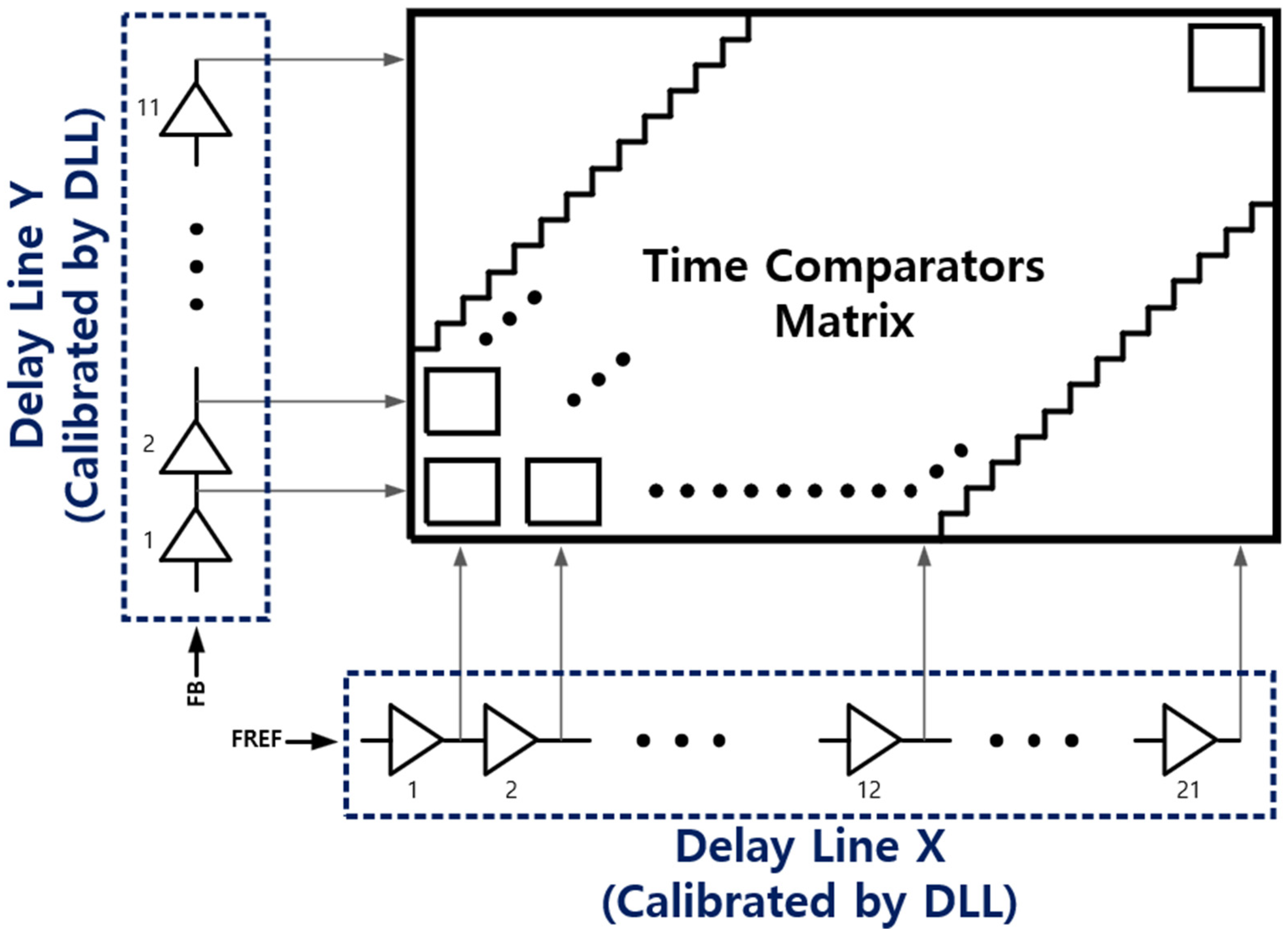
Figure 4 shows the block diagram of a two-dimensional time-to-digital converter. The time-to-digital converter (TDC) designed in this study is based on a two-dimensional Vernier architecture with a 7-bit thermometer output [
20]. This design significantly reduces the length of the delay line compared to traditional linear Vernier architectures, thereby mitigating the accumulation of jitter as the reference or feedback signal passes through the delay line. By utilizing two delay lines along the X and Y axes, this architecture allows for a shorter delay line while achieving the same bit resolution, resulting in superior area efficiency due to the two-dimensional layout design. In this design, the X-axis delay line has a delay of 38.5 ps per stage, while the Y-axis delay line has a delay of 35 ps per stage, achieving a TDC resolution of 3.5 ps. This resolution is attained through the difference between the delay steps of the X and Y delay lines. The two-dimensional structure generates a Vernier plane with a higher number of quantization levels, enhancing the time range that the TDC can detect.
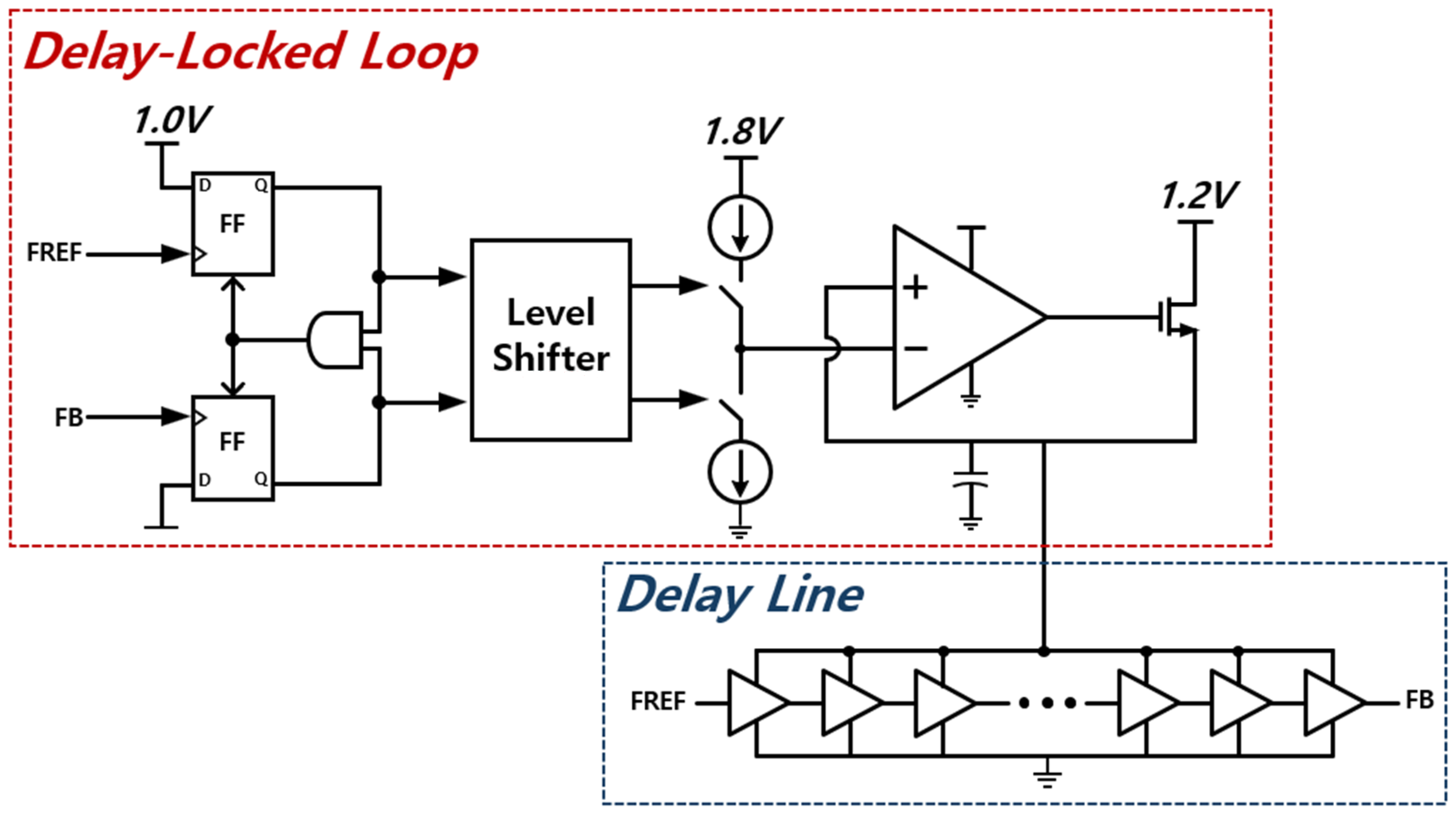
A critical challenge in designing high-resolution TDCs is maintaining consistent performance across process, voltage, and temperature (PVT) variations. Traditional Vernier TDCs can exhibit significant resolution changes due to PVT variations. To address this, the designed TDC incorporates a delay-locked loop (DLL) to ensure the delay of the delay lines.
Figure 5 shows the block diagram of the delay-locked loop (DLL). The calibration process includes feedforward calibration, where the DLL adjusts the supply voltage (VDD) of each delay line through a low-dropout (LDO) regulator, ensuring the X delay line consistently achieves 38.5 ps and the Y delay line consistently achieves 35 ps. This approach stabilizes the TDC resolution at 3.5 ps despite PVT variations.
The proposed low-power, compact wideband PLL architecture employs a ring oscillator (RO) type oscillator, which has a smaller area than an LC oscillator. However, ROs generally exhibit higher phase noise. To mitigate the out-of-band phase noise generated by the RO, the PLL’s bandwidth is extended to effectively suppress out-of-band noise. This approach increases the in-band noise tolerance, necessitating a high-resolution TDC to maintain overall noise performance. The two-dimensional Vernier TDC achieves a resolution of 3.5 ps, thereby reducing in-band phase noise and enhancing the overall performance of the PLL. The implementation of the two-dimensional Vernier TDC begins with the design of a time comparator that compares signals from the X and Y delay lines using flip-flops. The output of this comparator is sequentially ordered and output as a thermometer code. The proposed two-dimensional Vernier TDC provides a compact and efficient solution for high-resolution time-to-digital conversion. By combining a two-dimensional delay line structure with a robust calibration mechanism, it ensures stable and accurate performance, making it suitable for integration into wideband PLLs with stringent area and noise requirements.
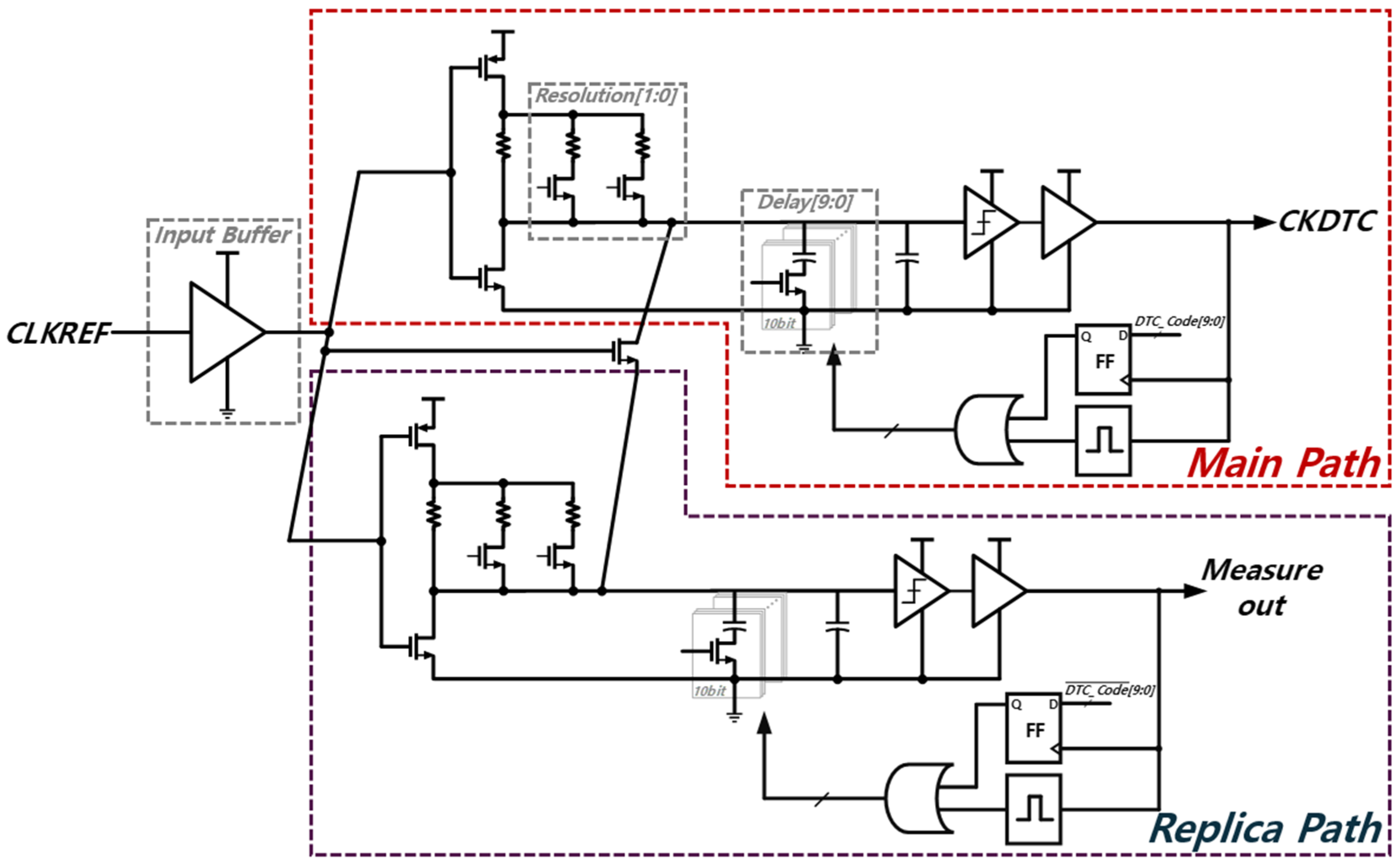
3.3. DTC
Figure 6 shows the block diagram of an RC delay-based digital-to-time converter. To support the fractional-N functionality of the PLL using the QE values obtained from the delta-sigma modulator, a carefully controlled resistor–capacitor (RC)-based digital-to-time converter (DTC) architecture is employed, ensuring stable and predictable delay characteristics across the supported resolution settings [
21,
22]. This design incorporates a 10-bit control architecture for the DTC, with the control bits divided into two segments: the lower 5 bits (LSB) are binary encoded, while the upper 5 bits (MSB) use thermometer coding. This hybrid configuration combines the area efficiency of binary encoding with the linearity of thermometer encoding, thereby enhancing timing accuracy.
The DTC supports three resolution settings: 1.1 ps, 750 fs, and 360 fs. These resolutions are achieved by adjusting the timing characteristics of the delay line through resistor switches. At the most precise 360 fs resolution, the DTC delivers a phase noise performance of approximately −150 dBc/Hz at a 1 MHz offset, suitable for targeting high frequencies above 5.7 GHz in wideband PLLs. The 750 fs resolution setting provides a phase noise performance of −146 dBc/Hz at a 1 MHz offset, targeting frequencies from 2.7 to 5.7 GHz. The 1.1 ps resolution setting offers a phase noise performance of −140 dBc/Hz at a 1 MHz offset, covering frequencies from 2 to 2.7 GHz. The resolution and control bits of the DTC must be designed to match the period of the DCO and the quantization error (QE) pattern of the DSM. For instance, if a second-order delta-sigma MASH11 with a QE range of two is used and the DCO period is 300 ps, the DTC must cover a range of 600 ps, which is twice the DCO period. The coverage range of the DTC is determined by multiplying the DTC resolution by two raised to the power of the number of bits, necessitating the selection of an appropriate DTC resolution for the frequency band. In RC slope-based DTC designs, the relationship between DTC resolution and phase noise indicates that lower resolution improves phase noise, thus the appropriate DTC resolution must be selected based on the application. The designed DTC exhibits an integral nonlinearity (INL) of 4.5 LSB, demonstrating efficiency in performance. These design specifications ensure that the DTC provides high accuracy and minimal phase noise, enhancing the overall performance and reliability of the wideband PLL system.
The relationship between DTC resolution and phase noise in an RC slope-based DTC indicates that lower resolution improves phase noise. Thus, for high-frequency applications in wideband PLL designs, reducing the DTC resolution enhances PLL performance. With these design specifications, the DTC ensures high accuracy and minimal phase noise, contributing to the overall performance and reliability of the wideband PLL system.
5. Experimental Results
The locking simulation of the triple-loop wideband fractional-N all-digital phase-locked loop (WBPLL) is illustrated in
Figure 8. The ADPLL consists of three loops: the automatic frequency control (AFC) loop, the counter-assisted phase-locked loop (CAPLL), and the digital sub-sampling phase-locked loop (SSPLL). The locking process sequentially progresses through these three loops. In
Figure 8, the target frequency is set to 3.5 GHz. The simulation captures the operation of the WBPLL as it locks onto this frequency, demonstrating the coordinated functioning of the AFC, CAPLL, and SSPLL loops. These results highlight the effectiveness of the triple-loop architecture in achieving stable frequency locking. The verification of the locking process was conducted using SystemVerilog and Verilog-HDL modeling, incorporating post-simulation results from the time-to-digital converter (TDC), digital-to-time converter (DTC), and digitally controlled oscillator (DCO).
Figure 8 provides a detailed view of the locking stages, illustrating how each loop contributes to overall frequency stabilization. The AFC loop initially brings the frequency close to the target, the CAPLL refines it further, and the SSPLL ensures fine adjustments and long-term stability. Additionally,
Figure 9 shows the locking time for target frequencies ranging from 1.9 to 6.1 GHz, demonstrating the proposed WBPLL’s stable locking performance across this frequency range when approximately 5500 random target frequencies were input. These simulation results confirm the robustness and precision of WBPLL, demonstrating its reliability as a solution for broadband frequency applications requiring precise and stable frequency control.
In this study, it has been demonstrated that a wide range of frequencies can be synthesized using a ring oscillator (RO) structure instead of conventional LC structures.
Table 1 shows that our proposed architecture has an overwhelming frequency range of 4.2 GHz compared to prior-art RO frequency synthesizers. Despite achieving this impressive range, we successfully designed the chip with a very compact total area of 0.055 mm
2. The normalized area is included in the table because the minimum MOSFET length varies with different technologies. Due to the differing minimum lengths provided by each process, direct size comparisons may be unfair. Therefore, the total area has been normalized according to the minimum length provided by each process. The performance values in
Table 1 are derived using SystemVerilog and Verilog-HDL modeling, incorporating post-simulation results from the key cells of the PLL (DCO, TDC, DTC). Additionally, the IPN value meets −33.42 dBc within the 10 kHz to 10 MHz range, fulfilling the 5G FR1 requirements. This indicates that our proposed digital SSPLL can be utilized in various applications due to its wide frequency synthesis range, compact chip area, and satisfactory IPN performance.
Figure 10 shows the phase noise characteristics of the proposed WBPLL.
Figure 10 presents the results for each noise contribution simulated in the S-domain model based on the post-simulation design specifications, operating at 3.5 GHz. The phase noise graph refers to the phase noise spectrum of a Single Sideband (SSB) signal, with the starting point being the carrier frequency. This spectrum represents the power difference between the signal and noise, normalized in Hz, as a function of the offset from the carrier frequency. Therefore, it is used to predict the expected real noise. This detailed analysis demonstrates the ability of the WBPLL to maintain low phase noise, with an integrated phase noise of −33.42 dBc from 10 kHz to 10 MHz, across its operating range, further validating its suitability for high-performance applications. These results were obtained with the thermal noise of the input reference frequency at −153 dBc/Hz. Additionally, this phase noise performance is sufficient to support 5G FR1 networks and IoT applications, highlighting the effectiveness of the WBPLL in these advanced communication systems.
The proposed wideband PLL offers the advantage of a wide frequency tuning range within a small chip area. To achieve this compact size, the oscillator is designed based on a ring oscillator (RO) instead of an LC-based oscillator. Although RO has poorer out-band noise characteristics compared to LC oscillators, increasing the reference frequency and loop bandwidth can suppress the out-band noise from the RO effectively.
6. Conclusions
This paper presented a wideband fractional-N all-digital phase-locked loop (WBPLL) architecture that utilizes a triple-loop configuration to achieve frequency tuning from 1.9 to 6.1 GHz. The architecture employs the automatic frequency control (AFC) and counter-assisted phase-locked loop (CAPLL) in the first and second loops for coarse locking, while the third loop utilizes a digital sub-sampling architecture without a frequency divider for fine locking. Fractional-N frequency synthesis in the third loop is accomplished using a delta-sigma modulator (DSM) and a digital-to-time converter (DTC). The reuse of digital modules such as counters, comparators, and differentiators across the AFC and CAPLL loops significantly minimizes the area requirement. Moreover, the introduction of a moving average filter (MAF) effectively reduces the frequency overlap ratio of the digitally controlled oscillator (DCO) between the second and third loops, ensuring stable and reliable loop switching. The total power consumption of the WBPLL varies with the frequency range, consuming between 8.8 mW at the WBPLL minimum output frequency of 1.9 GHz and 12.8 mW at the WBPLL maximum output frequency of 6.1 GHz, all at a 1.0 V supply. Implemented in a 28 nm CMOS process, the WBPLL achieves an impressive area efficiency, occupying only 0.055 mm2. The experimental results verify the robustness and precision of the WBPLL, demonstrating its suitability for high-performance applications. The phase noise performance and locking capabilities of the proposed architecture confirm its potential to support advanced communication systems such as 5G FR1 networks and IoT applications, making it a highly viable solution for modern frequency synthesis requirements.


