Article

Digitally Controlled Fractional-Order Elements Using OTA-C Structures

by
Edi Emanovic
1,
Marijan Vonic
1,
Drazen Jurisic
1,* and
Costas Psychalinos
2
1
Faculty of Electrical Engineering and Computing, University of Zagreb, HR-10000 Zagreb, Croatia
2
Electronics Laboratory, Department of Physics, University of Patras, GR-26504 Rio Patras, Greece
*
Author to whom correspondence should be addressed.
Electronics 2024, 13(11), 2066; https://doi.org/10.3390/electronics13112066
Submission received: 6 May 2024 / Revised: 23 May 2024 / Accepted: 24 May 2024 / Published: 26 May 2024
(This article belongs to the Special Issue CMOS Integrated Circuits Design)

Abstract

:
This article presents an active realisation of an electronically controlled FO capacitor or a constant phase element (CPE) and an FO inductor (FOI) in the form of an integrated circuit. The realisation is demonstrated using an OTA-C structure in AMS 0.35 μm C35B4C3 technology. The same core is used for both realisations of CPE and FOI, and the angles can be realised in all four quadrants. The realisation of active constant-phase elements using OTAs with MOS transistors in the saturation region is proposed. The operating frequency is in the high range of 7–350 kHz, with a centre frequency of 50 kHz. A tuning method is proposed using different bias currents of the OTAs, which in turn are digitally controlled to obtain the desired parameters such as impedance and angle of an element. The linearisation of the individual OTAs is achieved by source degeneration. The newly introduced minimax approximation is used to design three non-integer orders of 1/3, 1/2, and 2/3. The integrated circuit was designed with a total area of 710 × 1127 µm2. The power consumption of the entire system is 12.37 mW.

1. Introduction

In recent decades, fractional-order (FO) systems have emerged in interdisciplinary research as systems of the 21st century that represent continuous-time linear systems more efficiently than integer-order (IO) systems [1,2]. They efficiently describe processes in control theory, material theory, diffusion theory, robotics, signal processing, viscoelasticity, etc. The wide range of applications includes electrical filters [3,4], analogue modelling of bioimpedance [5], emulation of an electrical analogue model of the human body [6], food quality [7], DC-DC converters [8], applications in control theory for drive motors [9], analogue modelling of supercapacitors [10], analogue modelling of lithium batteries in electric vehicles [11], and many others.
In the design of the FO filters, the slope of the transition between the passband and stopband is defined by the relationship 20 · (n + α), where n is an integer and α is the fractional-order parameter, where 0 < α < 1. The dependence of the slope on the fractional order α presents an additional degree of freedom and new versatility in filter design. Furthermore, the dependence of the filter cutoff frequency on various additional circuit parameters, such as the fractional order α, offers additional degrees of freedom in the design [12].
Due to the irreversible dissipation effects of real electronic components, such as capacitors and inductors, the fractional capacitor is also frequently used in the modelling and stability analysis of electrical circuits. Due to these dissipative effects, classical integer-order models of electrical circuits cannot accurately describe the complex dynamic behaviour of real systems [13].
Westerlund has shown that capacitors with dielectric can only be modelled accurately with FO derivatives [14], because nature works with FO derivatives [15].
This property of capacitors directly affects the modelling and measurement of supercapacitors, which can be fitted more precisely with an FO resistor–capacitor model than with a conventional resistor–capacitor model [10].
Another application for which a high-frequency, tunable FOE is required in the literature is, for example, the fractional-order DC-DC buck converter [8,16], which offers additional degrees of freedom and increases the flexibility of the design. If the conventional integer-order buck converter cannot be reduced to the required voltage gain by adjusting the duty cycle, the fractional-order buck converter can further reduce the voltage gain by adjusting the fractional order to meet the system requirements. Therefore, it can be used in practical situations that require higher system stability and lower voltage gain. The application of digitally controllable FOEs (implementing both CPE and FOI) to DC-DC converters operating at high frequencies is beyond the scope of this paper and will be explored in the future.
To create FO systems, a fractional order element (FOE) is required. Many researchers have recently been working intensively on the research topic of how to design elements with fractional order [17]. There are two main approaches in the literature: (i) single-component FOE (e.g., in silicon [18] or printed circuit boards immersed in solution [19]) and (ii) multi-component FOE (e.g., passive networks in [20]). In addition, researchers have attempted to realise electronically tunable FOEs in an integrated form consisting of multiple components (e.g., [21] and chapter 5 in [22]). The MOS transistors of the OTAs in [21] operate in the sub-threshold (weak inversion) region. The operating frequency of these circuits is very low and is suitable for biomedical applications where the frequencies are very low.
The realisation of fractional-order elements such as an FO capacitor or a constant-phase element (CPE) and an FO inductor (FOI) starts with the transfer function H(s), which represents a differentiator or integrator. It is included in a V/I converter (another OTA), which then converts the transfer function H(s) into a driving point impedance Z(s). It was defined for the first time in [22], and then used in [23], etc. In the applications in [22,23], the frequency range is quite low and within the bandwidth of two decades, i.e., between 10 Hz and 1 kHz. Since the operating frequency of these circuits is low, the MOS transistors of the OTAs operate in the sub-threshold region and therefore consume low power. In [5], the FO (Cole-Cole) model of biceps tissue during fatigue exercise was described, and the frequency range is between 10 kHz and 100 kHz. Therefore, as shown in [5], at the higher operating frequencies, the OTAs must be used with transistors biassed in the strong inversion region. The high-frequency range comes at the price of higher power consumption.
If the FOE is built as an active element, it is possible to tune the FOE order with different bias currents for OTAs. In this paper, we will extend the idea from [21,22] to tune the parameters of FOEs using digitally controlled bias currents. We will also extend the idea from [21,22] to the realisation of integrated FOEs with OTAs operating with MOS transistors in the strong inversion region. The OTAs in this paper are linearised using source degeneration, as in [24,25]. The optimal operating conditions for the OTAs are presented. The preliminary results of this paper can be found in [26].
The contributions in this paper are: (i) the use of minimax (MMX) [27,28] to obtain a more cantered approximation to the phase than the continued fractional expansion (CFE) approximation [29]; (ii) the proof of concept of constant phase element (CPE) that works at high frequencies and with MOSFETs in strong inversion; (iii) the digital tuning of the angle of the CPE; (iv) the design of the CPE to achieve minimum bias current spread with different OTA topologies; and (v) the linearisation of single-stage OTAs designed for high linearity and stability and the use of cascode mirrors for high output impedance. Although the proposed circuit can provide FOE angles in all four quadrants using the same core, the presented solution demonstrates CPE only in the IV quadrant as proof of concept.
The paper is structured as follows: Section 2 describes a fractional order element and its basic definitions. Section 3 presents the design procedure for a fractional order element with OTAs and grounded capacitors using a practical example. Section 4 verifies the newly introduced design concept with the layout design and the post-layout analysis in Cadence as a proof of concept. Conclusions are drawn in Section 5.

2. Fractional-Order Impedance and Transfer Function

2.1. Basic Definitions

We first describe FOE, an element required in electrical circuits to become FO. Our approach to realising FOE is based on [22]. In this paper, we use OTAs with MOS transistors in a strong inversion region operating at higher frequencies.
The impedance of the FO capacitor or a constant phase element (CPE) of order 0 < α < 1 and the pseudo-capacitance Cα with the unit of [F · sα−1], where s is a second, is defined by:
Z C P E ( s ) = 1 C α s α ,
where (italic) s is the Laplacian operator (complex number). The impedance of the FO inductance (FOI) of order 0 < β < 1 and the pseudo-inductance Lβ [H · sβ−1] is defined by:
Z F O I ( s ) = L β s β .
Note also that the transfer function,
H ( s ) = ( τ s ) q ,
represents the FO integrator when q < 0 and represents the FO derivator when q > 0, where 0 < |q| < 1, and the time constant is given by:
τ = 1 ω 0 .
In Equation (4), ω0 is the centre frequency around which the approximation is usually defined.
The design equations for a generalised system of order α are obtained by replacing the Laplacian operator sα in the transfer function of the FO system with its integer approximation.
The example of the nth-order approximation of H(s) in Equation (3) in the form of the IO transfer function is given by:
H ( s ) = ( τ s ) α A n ( τ s ) n + A n 1 ( τ s ) n 1 + + A 1 ( τ s ) + A 0 B n ( τ s ) n + B n 1 ( τ s ) n 1 + + B 1 ( τ s ) + B 0 ,
and it is defined within a few decades around the centre frequency ω0.
After some calculations, Equation (5) can be represented by:
H ( s ) = ( τ s ) α A n B n s n + A n 1 B n 1 τ s + A 1 B n 1 τ n 1 + A 0 B n 1 τ n s 2 + B n 1 B n 1 τ s + + B 1 B n 1 τ n 1 + B 0 B n 1 τ n .
Equations (5) and (6) represent an nth-order approximation H(s) of the Laplacian operator (τs)α. The IO transfer function H(s) can then be realised with standard IO circuits. If τ = 1 in Equation (4), H(s) is considered normalised.
The magnitude and phase of normalised ideal CPE for α = −1/3 (−30°), −1/2 (−45°), and −2/3 (−60°) are shown in Figure 1.

2.2. Realisation of the Approximation Transfer Function H(s) and the Impedance Z(s) of the nth-Order

The inverse follow-the-leader (IFLF) multi-feedback topology as in [21,22], constructed using OTAs as active elements and grounded capacitors, is an excellent candidate for the physical realisation of H(s) in Equations (5) and (6) and is shown in Figure 2. It realises the voltage transfer function with asymmetrical input and asymmetrical output.
The transfer function of the circuit in Figure 2 is given in Equation (7) (see also [21,22]).
H ( s ) = V o u t ( s ) V i n ( s ) = G n s n + G n 1 τ 1 s n 1 + + G 0 τ 1 τ 2 τ n s n + 1 τ 1 s n 1 + + 1 τ 1 τ 2 τ n ,
where vout and vin are small signal quantities designated in Figure 2. To realise a grounded FO capacitor (or FO inductor), we use the physical implementation of Equation (7) in the emulation scheme for Z(s) shown in Figure 3 and realise a grounded impedance as shown in [22].
The input impedance Z(s) of the emulator, which realises the grounded impedance in Figure 3 from the transfer function H ( s ) = V o u t ( s ) / V i n ( s ) obtained by the realisation in Figure 2 is given by:
Z ( s ) = V 1 ( s ) I ( s ) = 1 g m V I H ( s ) .
In order to construct a fractional-order capacitor, we have started with a fractional-order differentiator with the transfer function H(s) = (τs)α, where τ = 1/ω0 is defined in Equation (4). It can also be concluded that the impedance Z(s) of CPE and FOI at the centre frequency ω0 is equal to 1/gmVI. H(s) at centre frequency ω0 has unity gain.
If we compare Equations (1) and (8), we obtain the value of the emulated pseudo-capacitance:
C α = g m V I τ α .
The same reasoning can be applied when defining the value of the emulated pseudo-inductance, when H(s) = (τs)β, and by comparing Equations (2) and (8):
L β = 1 g m V I τ β .
The IFLF topology, which realises the voltage transfer function H(s) with differential input and asymmetrical output, is shown in Figure 4.
The transfer function of the circuit in Figure 4 is defined by Equation (11).
H ( s ) = V o u t ( s ) V i n _ d ( s ) = V o u t ( s ) V i n + ( s ) V i n ( s ) = G n s n + G n 1 τ 1 s n 1 + + G 0 τ 1 τ 2 τ n s n + 1 τ 1 s n 1 + + 1 τ 1 τ 2 τ n ,
where vout, vin+, and vin are small signal quantities designated in Figure 4. Note that the differential input is defined by vin_d =vin+vin. Also note that Equations (7) and (11) realise the same form of the transfer function. The only difference is that the latter has a differential input and an asymmetrical output, while the former has both an asymmetrical input and an asymmetrical output.
The emulation scheme for Z(s) shown in Figure 5 realises a floating impedance, as shown in [22].
The input impedance Z(s) of the emulator, which realises the floating impedance in Figure 5 from the transfer function H(s) shown in Figure 4, is given by:
Z ( s ) = V 1 ( s ) V 2 ( s ) I ( s ) = 1 g m V I H ( s ) .
The V/I converter in Figure 5 is realised by the V/I converter with differential output OTA #8 below.
The emulation of voltage-excited fractional-order capacitor and inductor impedances was shown in Figure 3 and Figure 5, but this topology is not able to emulate the current-excited behaviour of fractional-order impedances. The emulation of current-excited CPE/FOI is described in Chapter 5.3 in [22].

2.3. Second-Order Realisation of the Approximation Transfer Function H(s) and the Impedance Z(s)

Equations (5) and (6) represent an nth-order approximation H(s) of the Laplacian operator (τs)α, and the example of the second-order approximation H(s) in Equation (3) in the form of the IO transfer function is given by:
H ( s ) = ( τ s ) α A 2 ( τ s ) 2 + A 1 ( τ s ) + A 0 B 2 ( τ s ) 2 + B 1 ( τ s ) + B 0 ,
and it is defined within a few decades around the centre frequency ω0, which is defined above as τ = 1/ω0 in Equation (4).
Equation (13) can also be represented by:
H ( s ) = ( τ s ) α A 2 B 2 s 2 + A 1 B 2 1 τ s + A 0 B 2 1 τ 2 s 2 + B 1 B 2 1 τ s + B 0 B 2 1 τ 2 .
The second-order transfer function H(s) in Equation (13), which is an approximation of (τs)α as shown in Equation (5), can be realised with the IFLF structure shown in Figure 4, which is adapted to the second order. The corresponding second-order signal-flow graph (SFG) is shown in Figure 6.
Using Mason’s (general) multi-path reduction rule for SFGs, we can calculate a transfer function T between any two nodes in the SFG [30,31]. Mason’s general rule is as follows:
T = 1 Δ k P k Δ k ,
where Δ is the graph determinant of the form Δ = 1 − (sum of all loops taken one at a time) + (sum of the products of all non-touching loops taken two at a time) − (sum of all non-touching loops taken three at a time) + …., Pk is the gain of the kth forward path, and Δk is the part of the graph determinant that contains only loops that have no common nodes with the path Pk.
For the SFG in Figure 6, we have obtained the following transfer function using Equation (15), which is given by:
H ( s ) = V o u t ( s ) V i n ( s ) = G 2 s 2 + G 1 τ 1 s + G 0 τ 1 τ 2 s 2 + 1 τ 1 s + 1 τ 1 τ 2 .
The definition of the time constants in Equation (16) is given by:
τ 1 = C 1 g m 1 ,   τ 2 = C 2 g m 2 .
The SFG manipulations applied to the SFG in Figure 6 to build the most effective circuit are described in [26]. The most effective is: (i) the repeatability of the same OTA element in as large a number as possible; (ii) the spread of transconductance values and bias currents is minimised. The final SFG is shown in Figure 7 and corresponds to the circuit realisation in Figure 8. The node voltages in the SFG labelled with red numbers are also written as green labels V in the OTA-C circuit.
The transfer function of the IFLF OTA-C part in Figure 8 without the V/I converter in the dashed box is defined by the second-order version of H(s) in Equation (7). It is identical to the realisation of the voltage transfer function H(s) in Equation (16), which results from the SFGs in Figure 6 and Figure 7. The definition of the time constants in Equation (17) is included.
The realisation of FOC begins with the introduction of Equation (13) in Equation (8), and we have:
Z ( s ) = 1 g m V I B 2 ( τ s ) 2 + B 1 ( τ s ) + B 0 A 2 ( τ s ) 2 + A 1 ( τ s ) + A 0 .
Note that τ1, τ2, G0, G1, and G2 belong to the IFLF transfer function (as Equation (16)), while A0, A1, A2, B0, B1, B2, and τ belong to the start transfer function, which realises the FO transfer function (as Equation (14)). We therefore calculate the parameters τ1, τ2, G0, G1, and G2 of the IFLF circuit from the parameters of the FO transfer function A0, A1, A2, B0, B1, B2, and τ.
If we compare the coefficients of Equation (16) with Equation (14), we obtain:
G 2 = A 2 B 2 ; G 1 τ 1 = A 1 B 2 1 τ ; G 0 τ 1 τ 2 = A 0 B 2 1 τ 2 ; 1 τ 1 = B 1 B 2 1 τ ; 1 τ 1 τ 2 = B 0 B 2 1 τ 2 ,
from which we have the design equations:
G 2 = A 2 B 2 ; G 1 = A 1 B 1 ; G 0 = A 0 B 0 ; τ 1 = B 2 B 1 τ ; τ 2 = B 1 B 0 τ .
As soon as we know the parameters τ1, τ2, G0, G1, and G2 of the IFLF from Equation (20), we select Ci and calculate gmi (i = 1, 2) from Equation (17) with:
g m 1 = C 1 τ 1 ,   g m 2 = C 2 τ 2 .
In the next section, it will be shown that the design of the IFLF multi-feedback FOE with OTA-C, as shown in Figure 8, requires too large transconductances gm and capacitances Cs for a given frequency range if not designed properly. Therefore, the simplest single-stage OTAs are used, which have moderate transistor dimensions and bias currents to save space and power consumption. The goal is to minimise the spread of gm values and use as many identical OTAs as possible in the circuit. The topology in Figure 8 is used because it suggests the same value for gm2 in four OTAs: #1, #2, #4, and #6 (note: G1 = 1). The use of different capacitance values (C1 and C2) is preferable in the design in order to obtain as many identical OTAs as possible with minimal gm dispersion.

3. Design Procedure

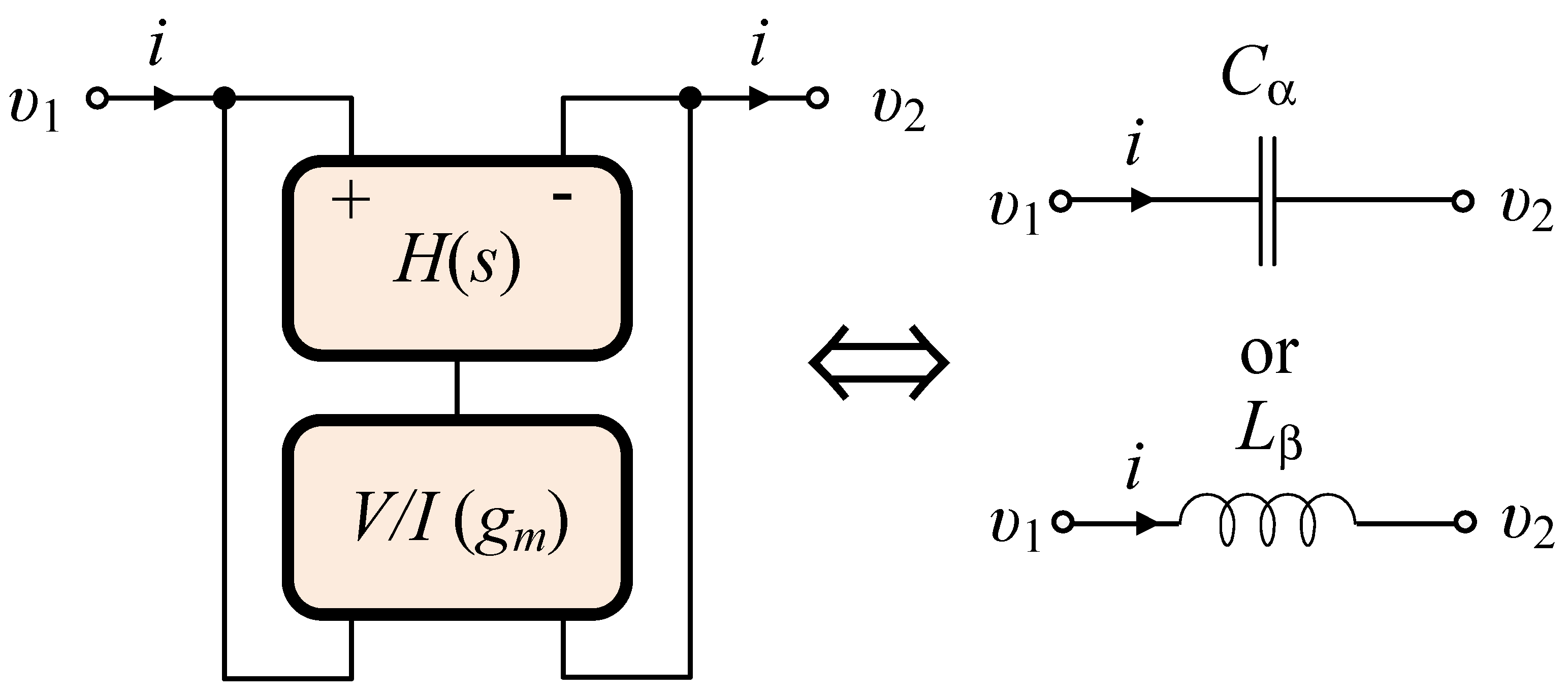
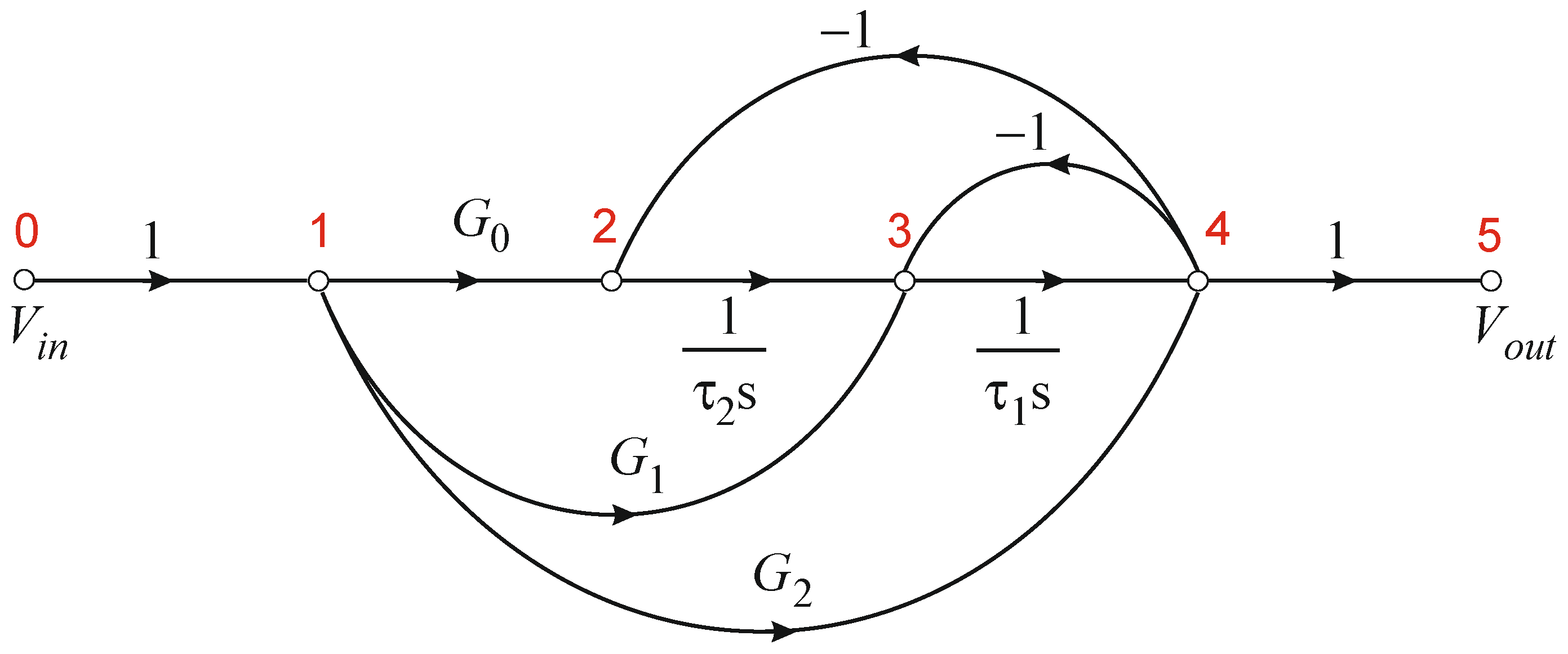
3.1. Approximations: Two Examples
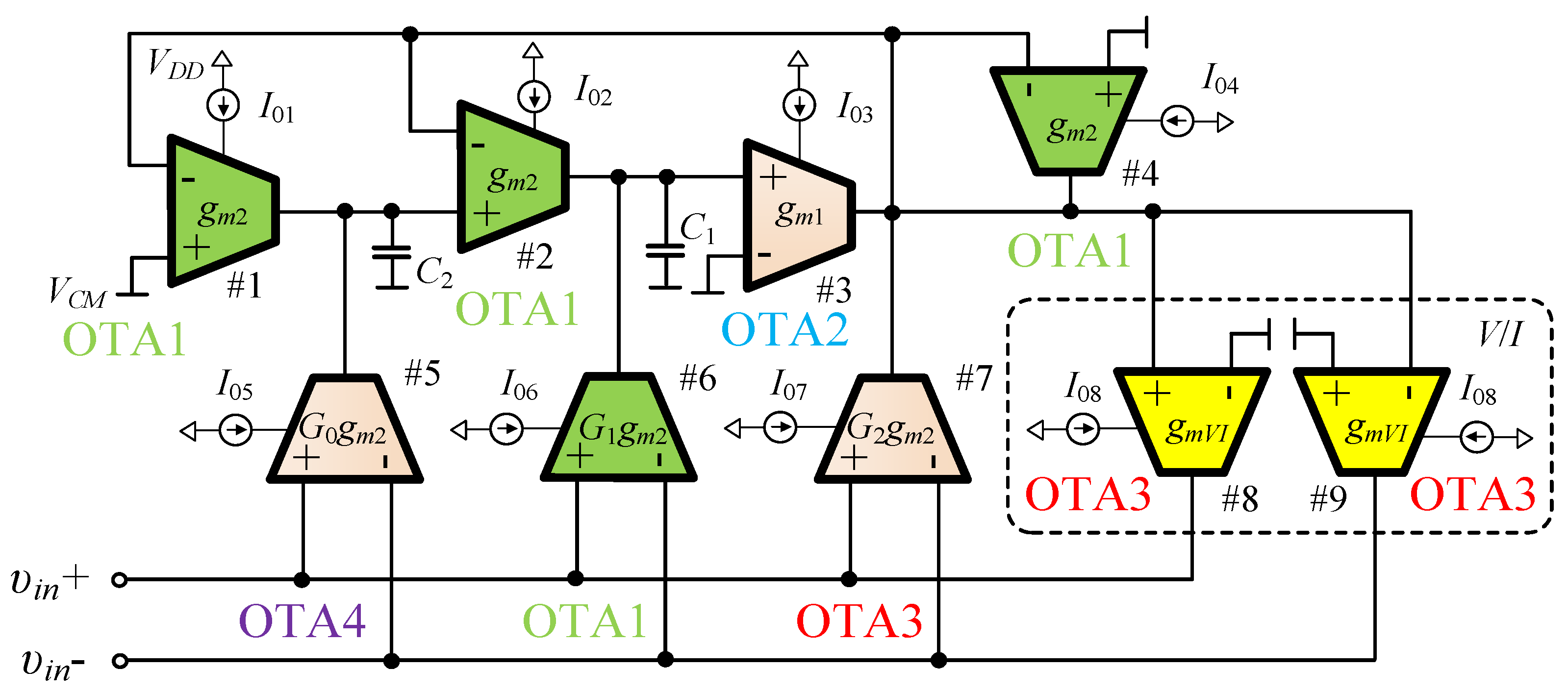
The circuit in Figure 8 is designed for α = −1/2, with the centre frequency f0 = 50 [kHz] and the CPE capacitance C = 500 [pF] at f0. Note that ω0 = 2πf0 = 100π [krad/s].
For Example 1, the second-order approximation with the continued-fractional expansion (CFE) as in [29] is used. The values obtained are the same as in [26] and are repeated in Table 1 in this paper. For Example 2 in this paper, the recently introduced minimax approximation from [27] is used. The Matlab R2021b (academic use) programme Ver. 1.0.1 in [28] can be used to calculate the minimax coefficients. Then the minimax approximation is compared with the CPE approximation used in [26].
The frequency analysis is performed from 5 kHz to 500 kHz because the centre frequency is at 50 kHz, and the second-order CFE approximation is efficient within almost two decades. A minimax approximation was developed that covers the same bandwidth as CFE. Therefore, BW = ωH/ωL = 50 is used in the design along with the programme in [28]. The values ωH = 7.071 [rad/s] and ωL = 0.14142 [rad/s] represent the normalised upper and lower limits of the useful frequency range for approximating a constant phase. Note that when designing the minimax approximation, it is possible to define the bandwidth BW, while this is not possible when designing CFE. The coefficients of H(s) for the second-order CFE and minimax approximations for the three values of α = 1/3, 1/2, and 2/3 are given in Table 1.
Note that the coefficients of the transfer functions in Table 1 are symmetrical. Therefore, from Equation (13) and τ = 1, the normalised coefficients of the transfer function H(s) are obtained for α = 1/2 from the second row in Table 1, given by:
A 2 = B 0 = 5 A 1 = B 1 = 10 A 0 = B 2 = 1 for   CFE , A 2 = B 0 = 5.03262 A 1 = B 1 = 10.4397 A 0 = B 2 = 1 for   MMX .
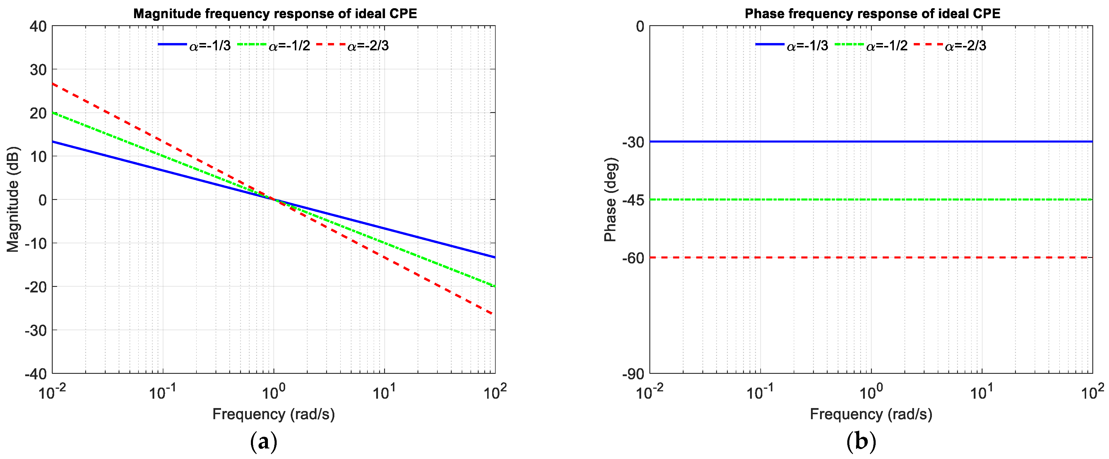
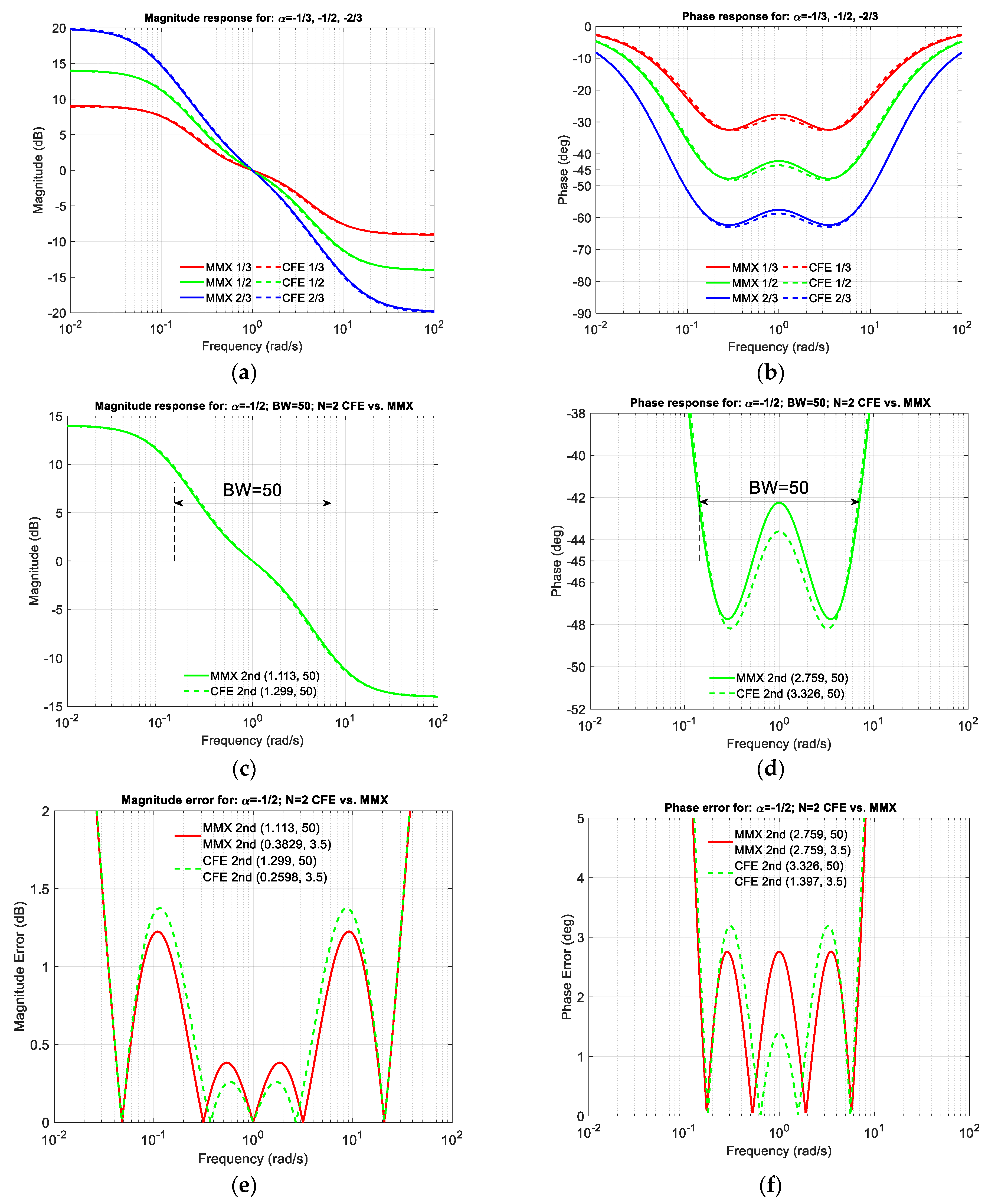
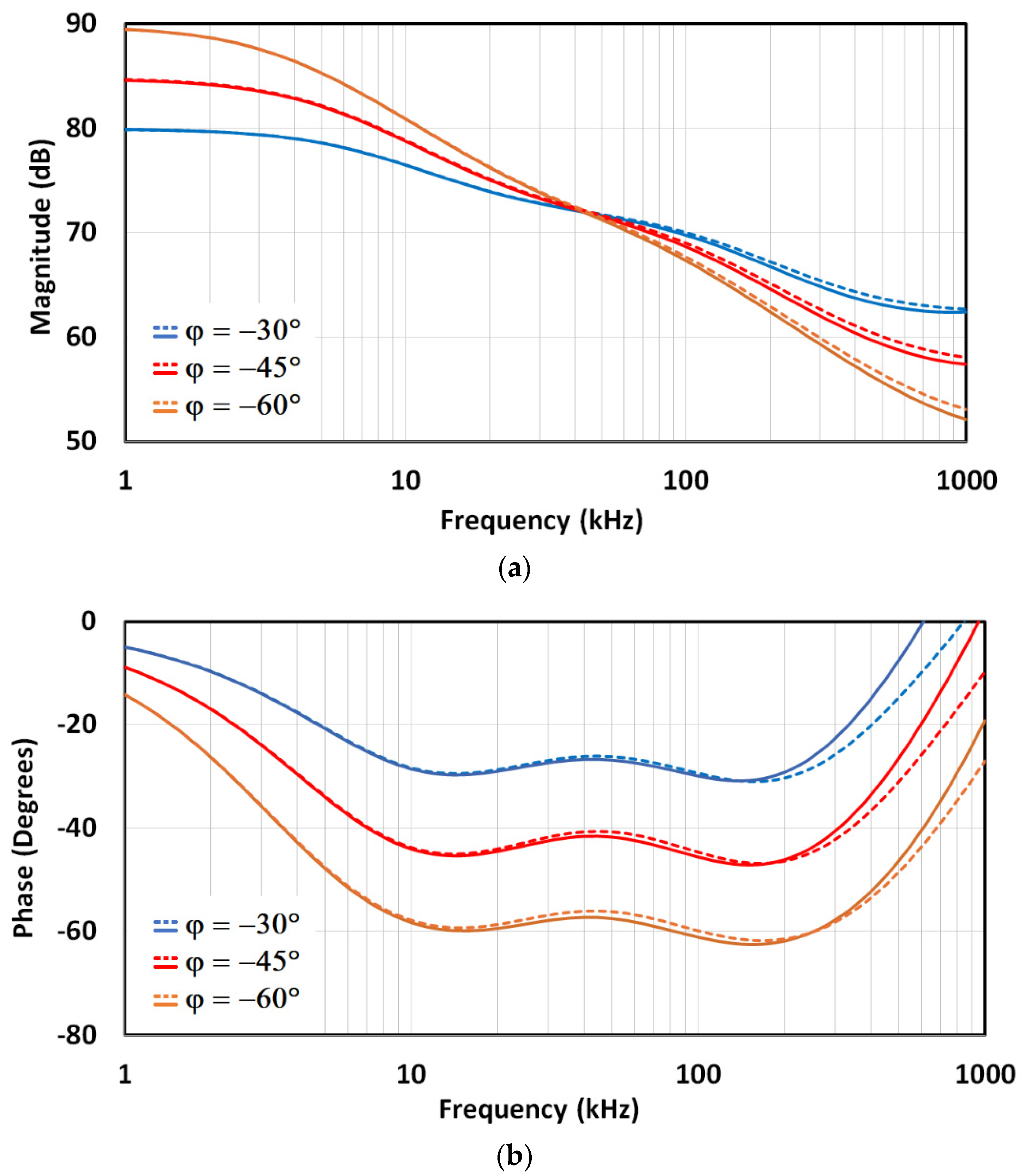
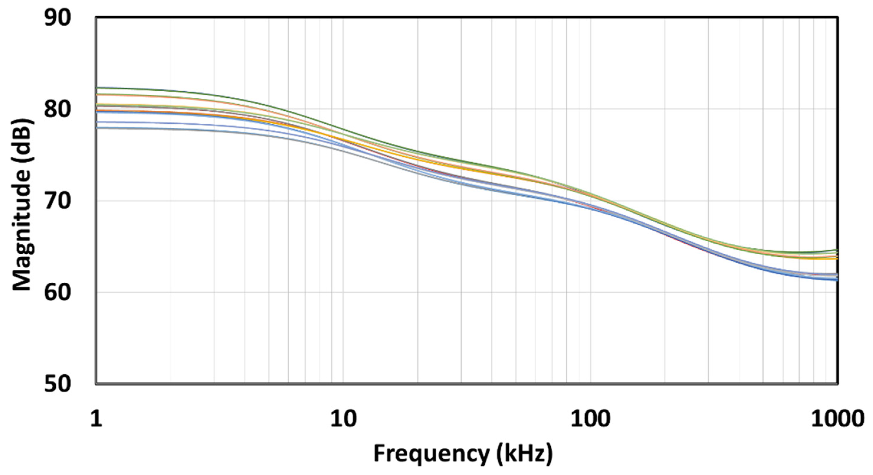
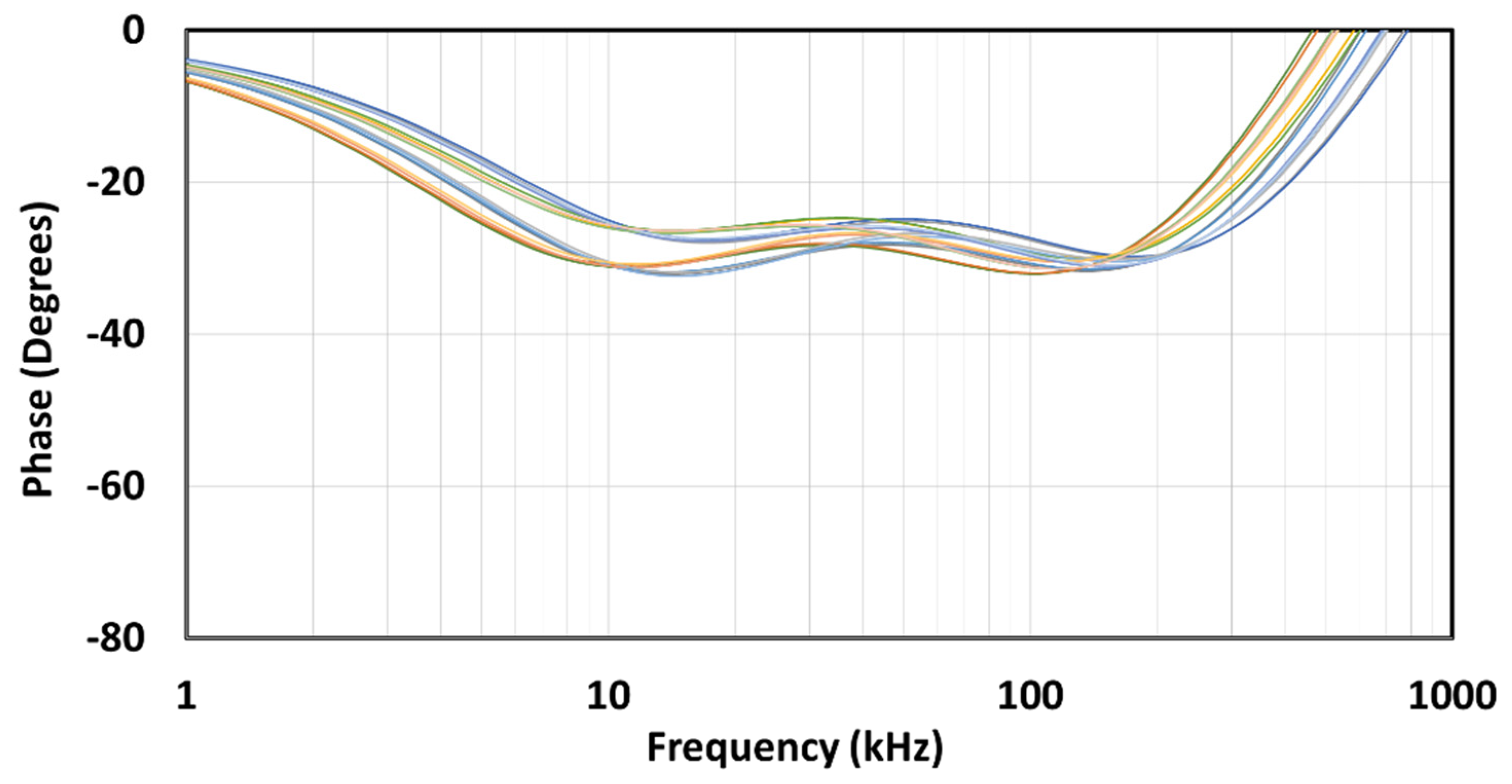
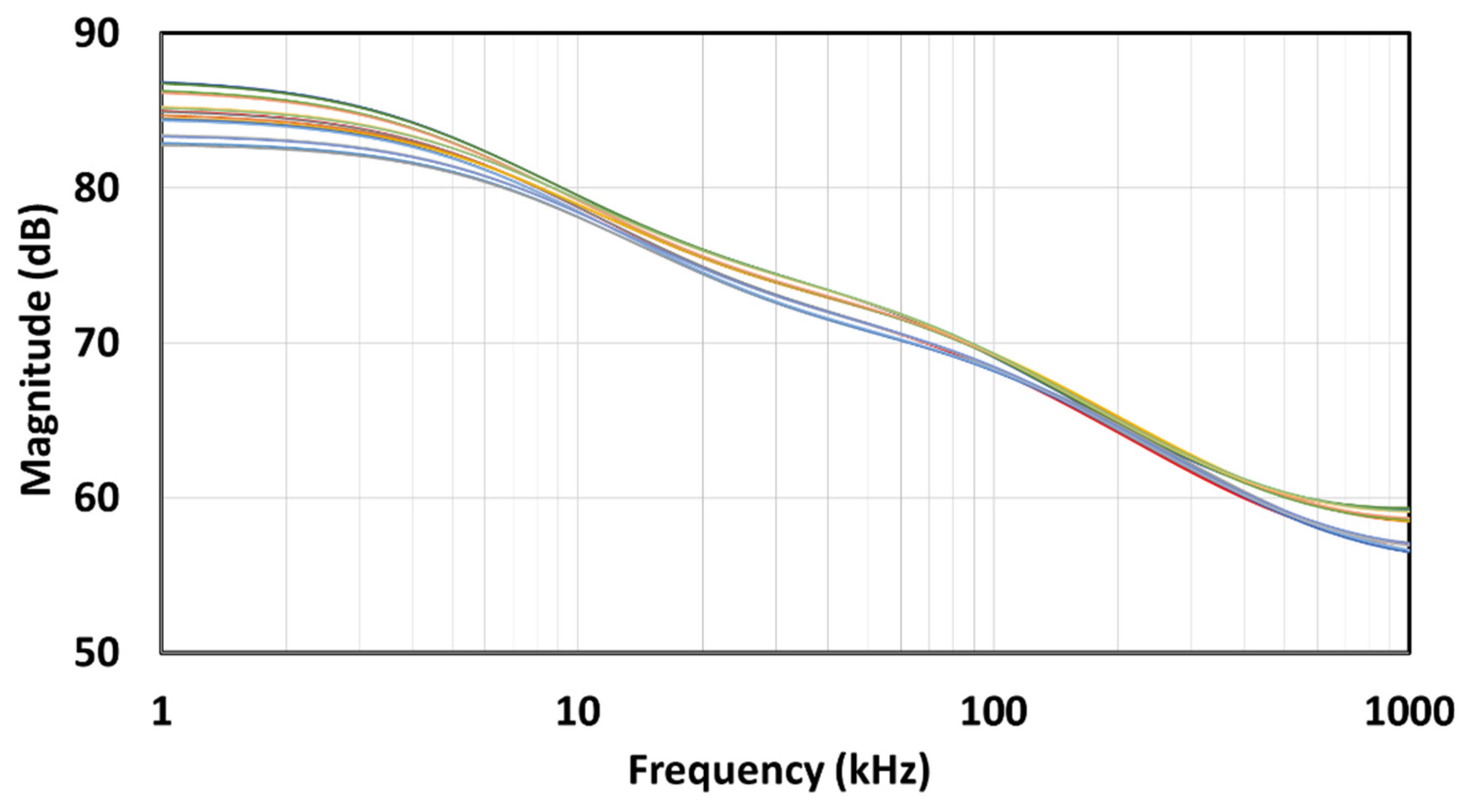
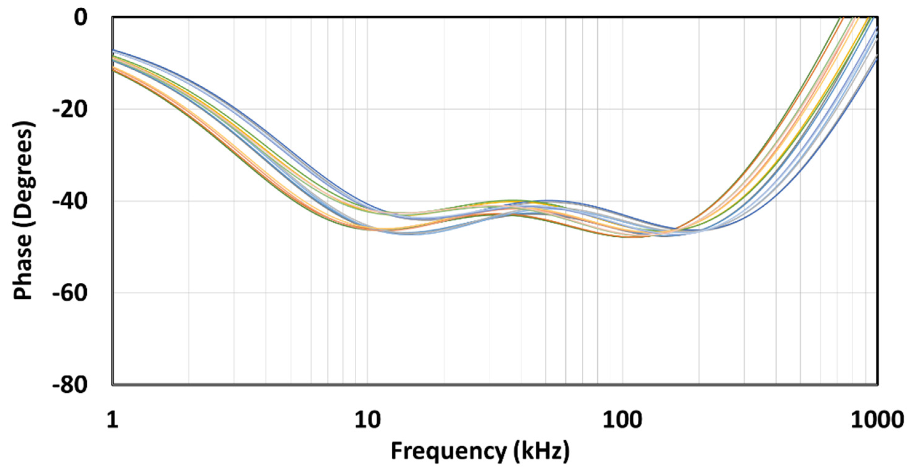
Normalised magnitude and phase of 1/H(s), where H(s) is defined for α = −1/3, −1/2, and −2/3, are shown in Figure 9. A detailed analysis for the case of α = −1/2 is also given. Recall that we must use 1/H(s) since in Equation (12), Z(s) is inversely proportional to H(s). Remember that the inverse of H(s) changes the sign of the angle from positive to negative.
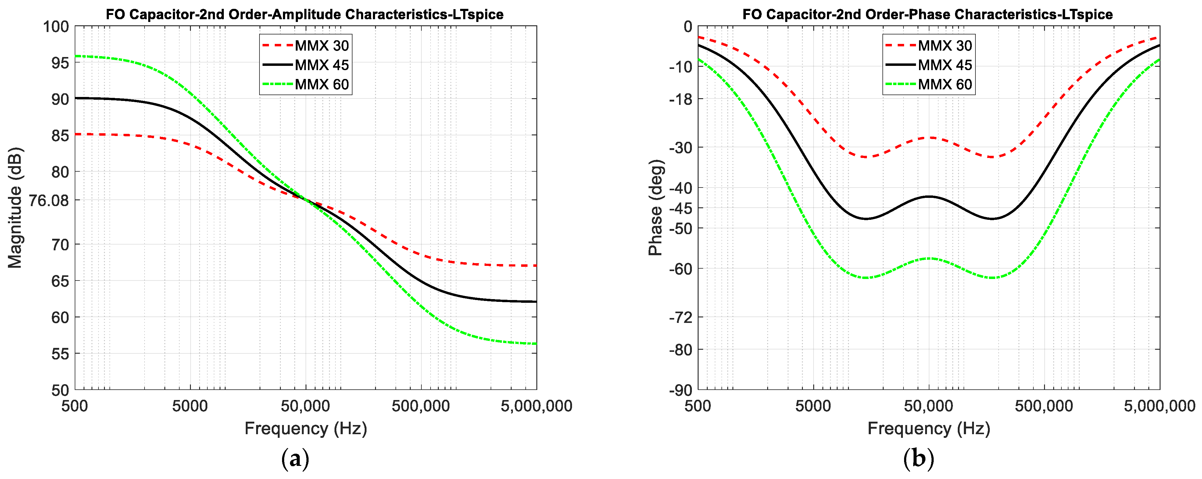
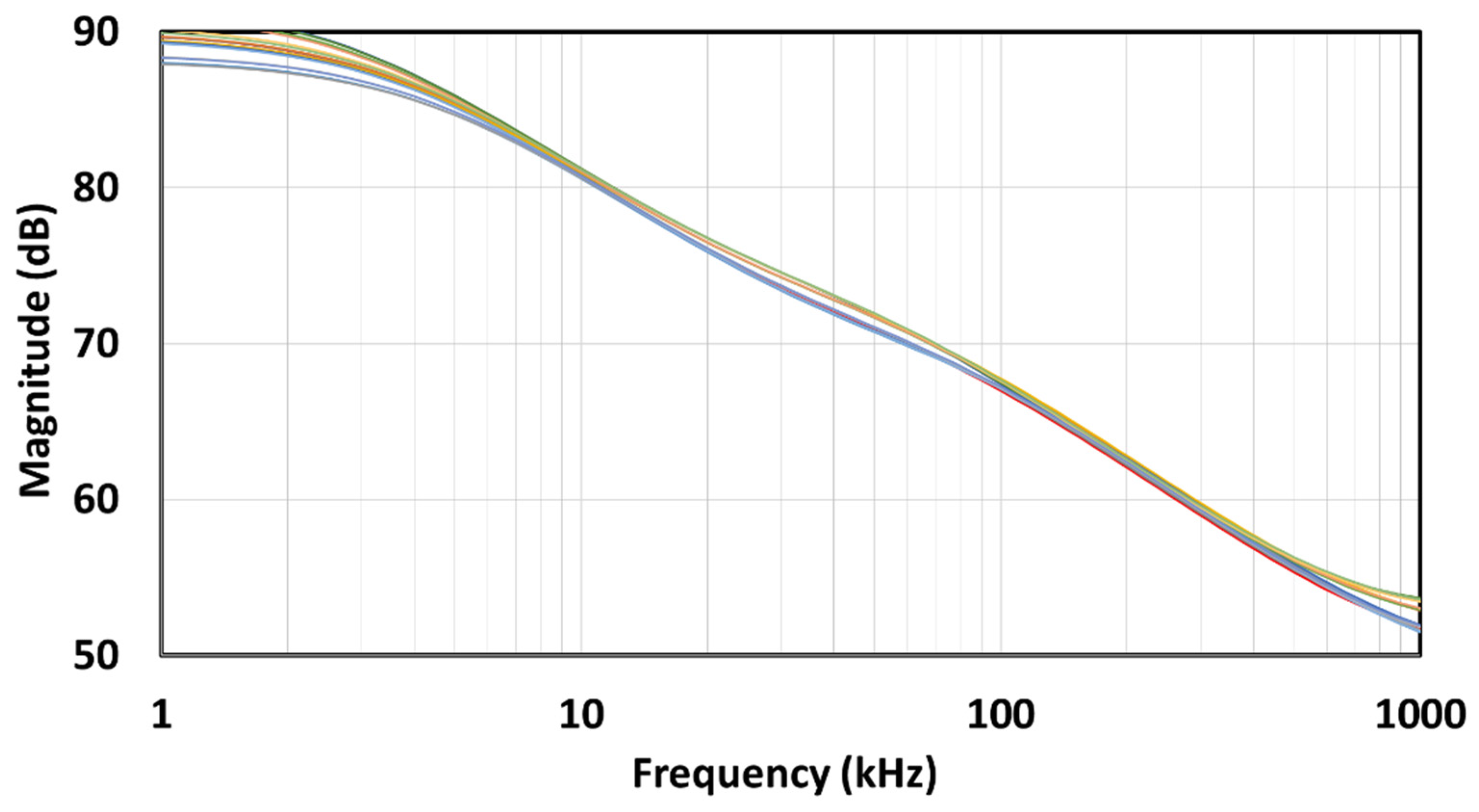
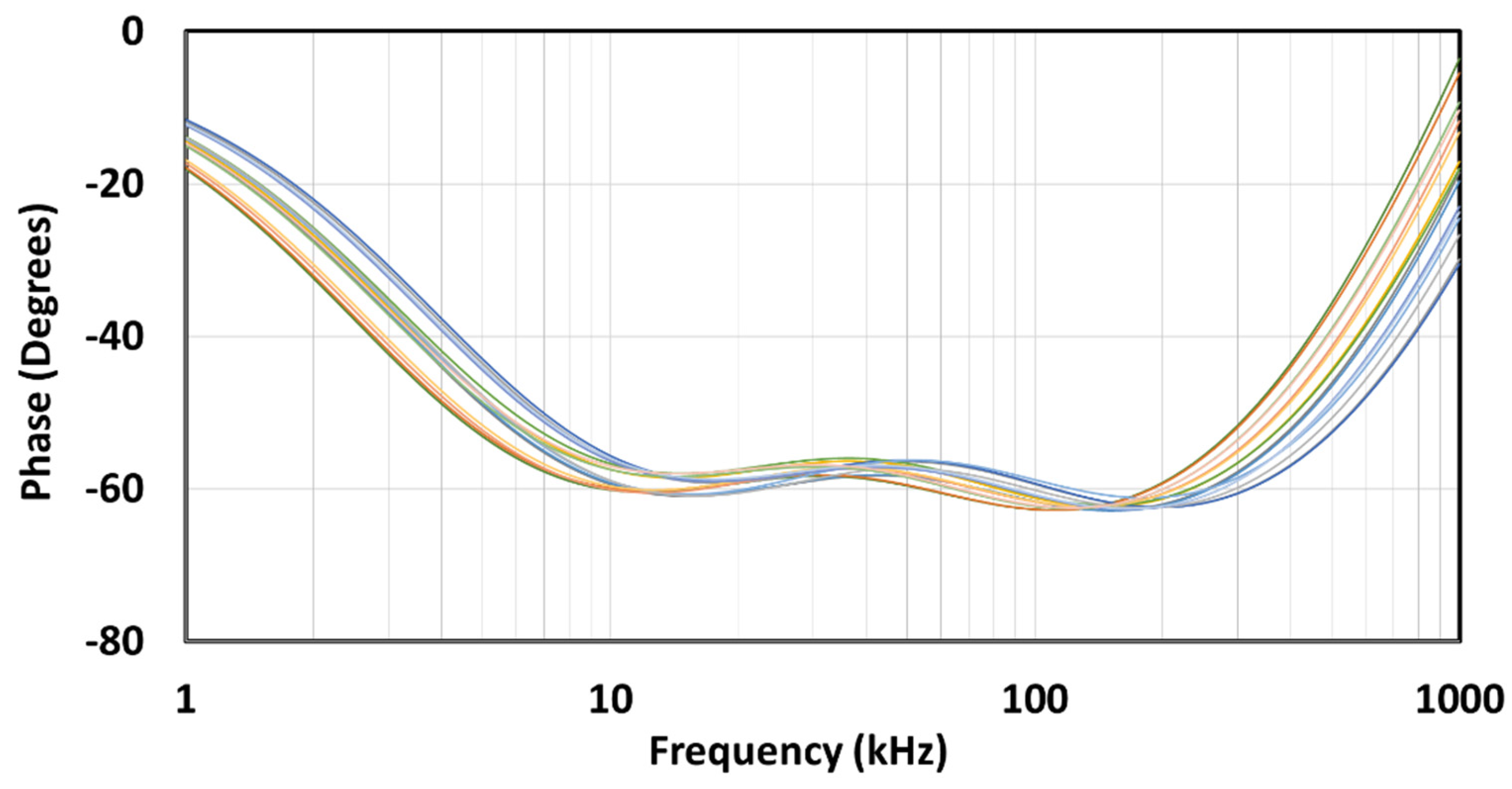
If we look at Figure 9a,b, we can see that there is a slight difference between the CFE and MMX approximations in both the amplitude and phase characteristics. In the zoomed amplitude response in Figure 9c, we can see this slight difference, while in the zoomed phase response in Figure 9d, we can see that the MMX is slightly more centred around the ideal phase of −45°. The values in brackets were determined numerically in Matlab R2021b (academic use) and represent the maximum deviation from the ideal value within the usable passband (BW = ωH/ωL = 50). In the case of MMX, it is 1.113 dB and 2.759°, while in the case of CFE, it is 1.299 dB and 3.326°. These values confirm that both the magnitude and phase curves of MMX are closer to the ideal than those of CFE when the entire usable frequency band is considered.
Figure 9e,f shows absolute amplitude and phase errors. The CFE is a better approximation near the centre frequency, while the MMX is a better approximation near the edges. Looking at the phase errors for the CFE, the absolute local peak-to-peak difference in phase is 3.326° + 1.397° = 4.723°, with the middle value −((3.326° − 1.397°)/2 + 45°) = −45.9645°, which represents the small phase offset from the desired −45°. In the case of MMX, the absolute local peak-to-peak difference in phase is 5.518°, which is worse than the CFE, but there is no phase offset. If a small phase can be added (or a small phase offset can be removed) in advance of the design process, the performance of the CFE can be better than that of the MMX.
In the following part of the paper, we will continue with the design of the MMX approximation in the CPE design.

3.2. Calculation of the CPE

Step-by-step design:
  • V/I converter in Figure 8: CPE capacitance at f0 = 50 [kHz] is C = 500 [pF], and therefore its transconductance is g m V I = C / τ = C ω 0 = 157.08 μ S , where ω 0 = 2 π f 0 .
  • The design of the circuit in Figure 8 follows for α = 1/2 (45°). From f0 = 50 [kHz], it is τ = 1 / ω 0 = 1 / ( 2 π f 0 ) = 3 . 1831 10 6 s . Using τ = 3 . 1831 10 6 s and Equation (22), we can write a denormalised H(s) as given by:
    H ( s ) = ( τ s ) 1 2 = 5.03262 s 2 + 3.27974 10 6 s + 9.8696 10 10 s 2 + 3.27974 10 6 s + 4.967 10 11 .
  • Including g m V I = 157.08 μ S and Equation (23) into Equation (8), fractional capacitance is:
    Z ( s ) = 1 157.08 10 6 s 2 + 3.27974 10 6 s + 4.967 10 11 5.03262 s 2 + 3.27974 10 6 s + 9.8696 10 10 ,
    and at the centre frequency of 50 kHz, it has the value 20 log ( 1 / g m V I ) = 20 log 1 / ( 157.08 10 6 ) = 76.08   dB . The corresponding pseudo-capacitance is given by C α = g m V I / ω 0 α F / s 1 α = 280.25 nF / s 0.5 . The denormalised upper and lower limits of the usable frequency range are fH = 350 kHz and fL = 7 kHz, while BW = fH/fL = 50 and f 0 = f L f H = 50 kHz.
The parameters of the IFLF circuit are calculated using the design Equations (17) and (20). If we judiciously choose capacitances, for example, C1 = 10 pF and C2 = 216.563 pF, then using Equation (21) we obtain equal values of gm for α = 1/2 (45°). The parameters for the IFLF structure are given in Table 2 and Table 3. The data for α = 1/2 (45°) can be found in the middle column. Note the ratios τ2/τ1 = B12/(B0 B2) = 21.6563 and G2/G0 = (A2 B0)/(A0 B2) = 25.3273, but gm1 = gm2 = 32.7974 μS.
As a double check before proceeding with the design of the transistors, Figure 10 shows the magnitude and constant phase characteristic of Z(s) obtained with the AC sweep analysis in LT-Spice using the parameters in Table 2 and Table 3. The impedance Z(s) in Equation (24) is represented by a solid black curve in Figure 10.
Although the achievable bandwidth is limited to the 7–350 kHz range, the reason for this lies in the rather low order of approximation. The use of this frequency range is useful for designing a fractional-order model of the biceps tissue during fatigue exercise [5]. To achieve a wider bandwidth, a higher-than-second-order approximation is required. The wider bandwidth would then be useful for the design of FO filters [3,4]. To properly design an FO filter, its cut-off frequency must be lower than the operating range of the CPE.

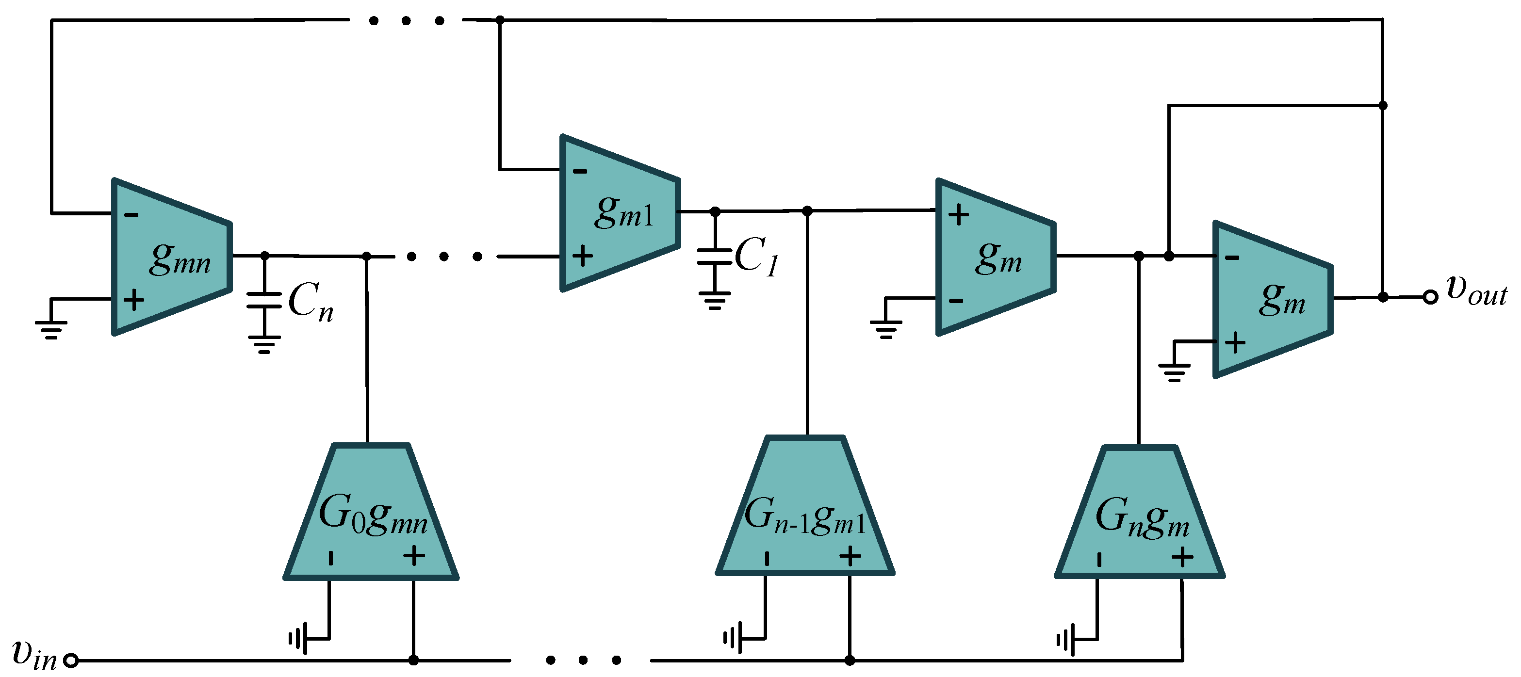
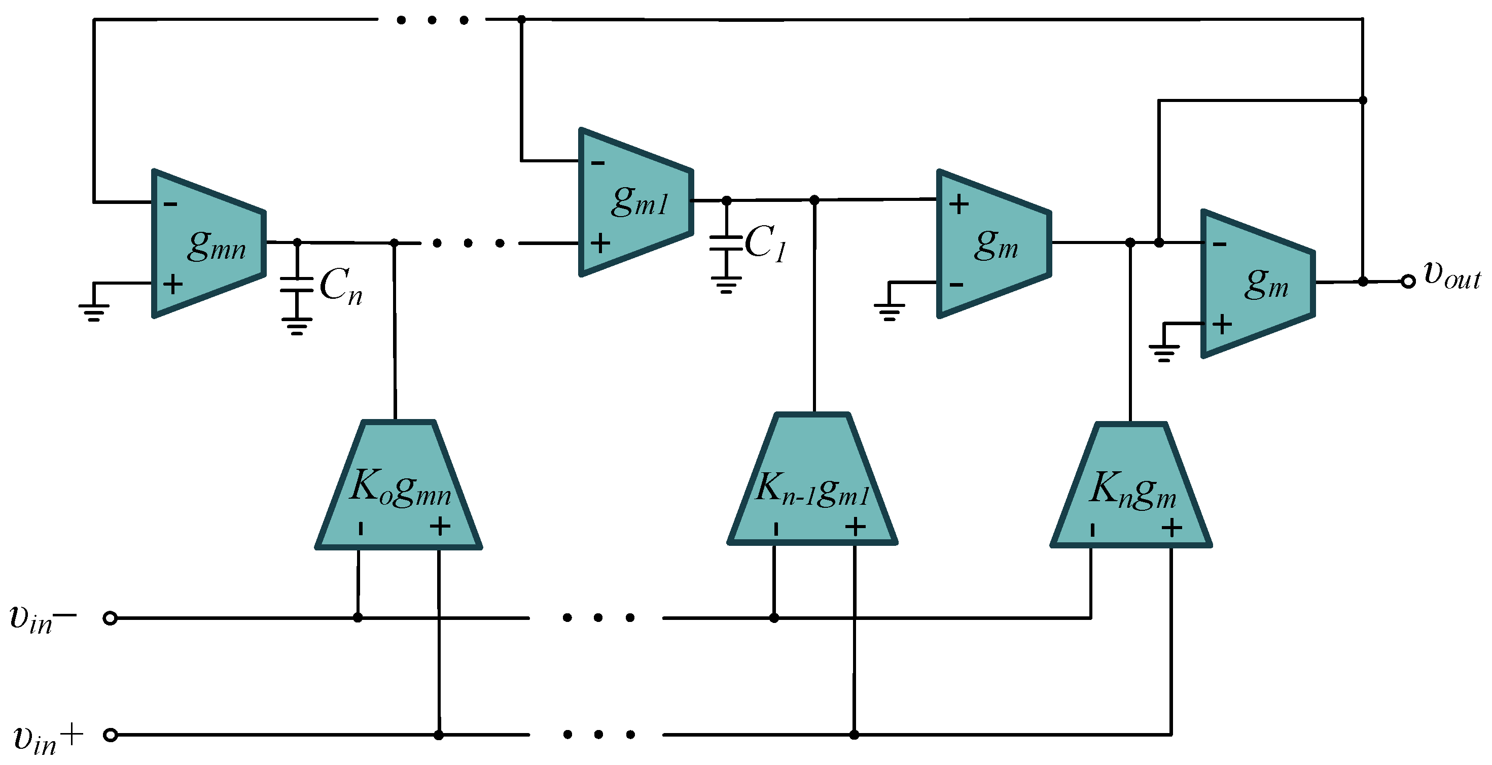
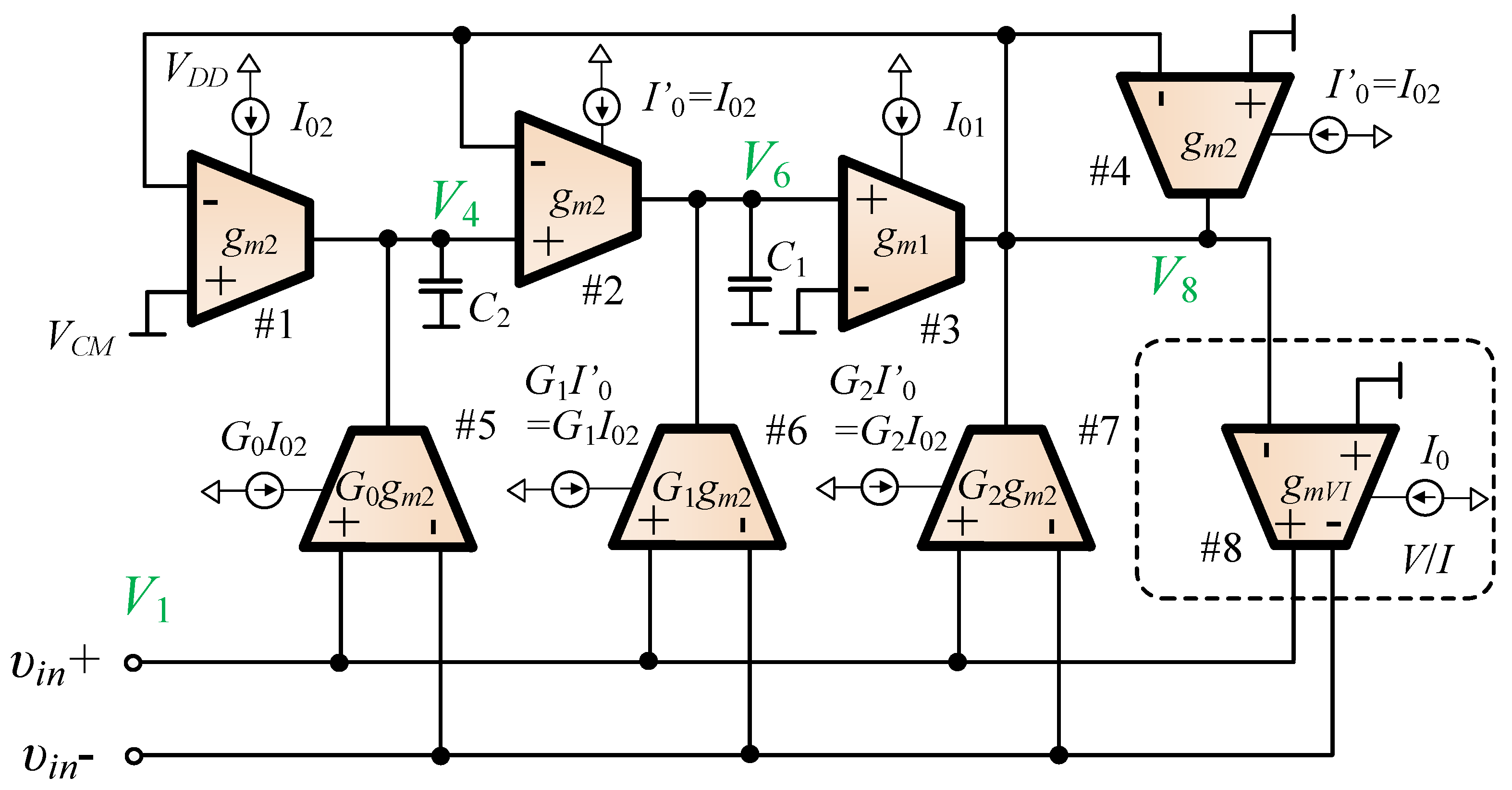
3.3. Designing of OTAs

In our paper, we will use OTAs with MOS transistors in the strong inversion region to operate at high frequency. The proposed OTAs are also referred to as gm cells with different gm values. OTAs (gm cells) are single-stage amplifiers for stability reasons, have a high output impedance because they have built-in cascodes, use source degeneration of the input diff pair by two MOSFETs operating in the triode region (see [24,25] and Section 14.1 in [32]), and use wide-swing current mirrors to have less headroom (see Section 6.3.1 in [33]).
The voltage supply is typical for the AMS 0.35 technology: VDD = −VSS = 2 V. First, we define a reference current Ibias in the acceptable value range for each OTA to be able to realise the required transconductances in Table 3. We consider that the source degeneration also reduces the resulting transconductance of the entire OTA compared to the transconductance of the input transistors. The optimum ratio between the dimensions of the input transistors and the dimensions of the degeneration transistors (the latter operate in the triode region) is N = (W/L)input/(W/L)deg = 6.7.
In the first step, we calculate the transconductances gm1,2 of the OTA input pair MN1,2 based on the required OTA transconductance gm with g m 1 , 2 = g m 1 + N / 4   = g m 1 + 6.7 / 4 = 2.675 g m . For example, to realise gm7=165.057 [μS] of OTA #7 in Figure 8, we need an input pair with gm1,2 = 2.675·165.057 [μS] = 441.53 [μS] in the electronic realisation of the OTA. This is a fairly high value.
To realise the given value of the transconductance, we decide between an NMOS or PMOS differential input stage, depending on the selected bias current Ibias and the acceptable dimensions of the input transistors. For a low value of the transconductance, we will use a PMOS input differential pair. For a medium value of transconductance, we will use an NMOS input differential pair. To achieve a high gm value and obtain a reasonable bias current, we will use an NMOS input differential pair and a symmetric CMOS OTA (see [5] and Chapter 7 in [34]). This means that we use three basic topologies of OTAs in our design, all of which are required to keep the bias currents within reasonable values. We distinguish between four versions of OTAs: OTA1 through OTA4. OTA1 and OTA2 are used for the realisation of medium 
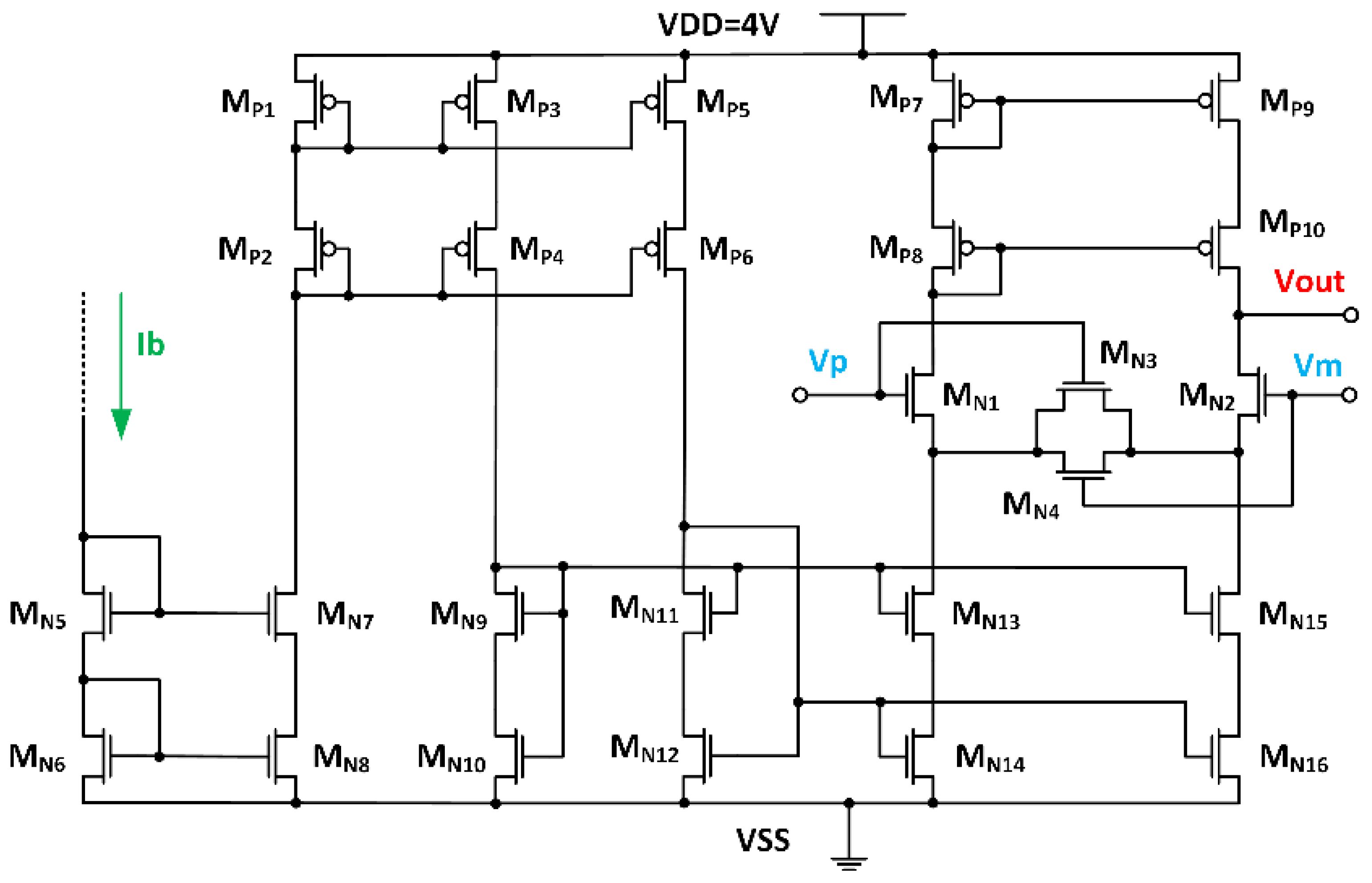
gm and have the same topology as shown in Figure 11, but differ only in the dimensions of the input NMOS diff pair. OTA3, which is shown in 
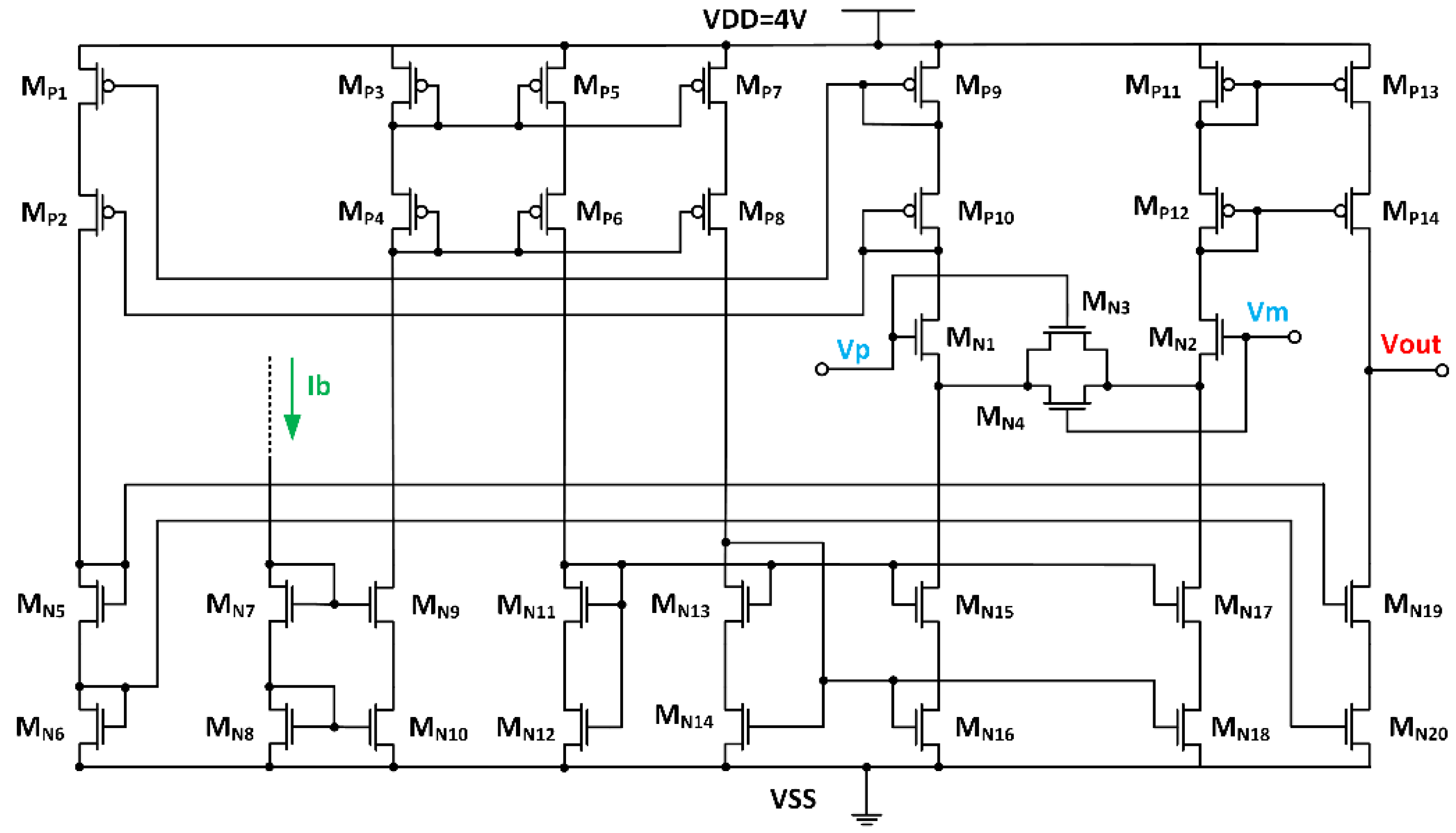
Figure 12, has a symmetrical CMOS OTA topology and is used for high gm values, and OTA4, which is shown in 
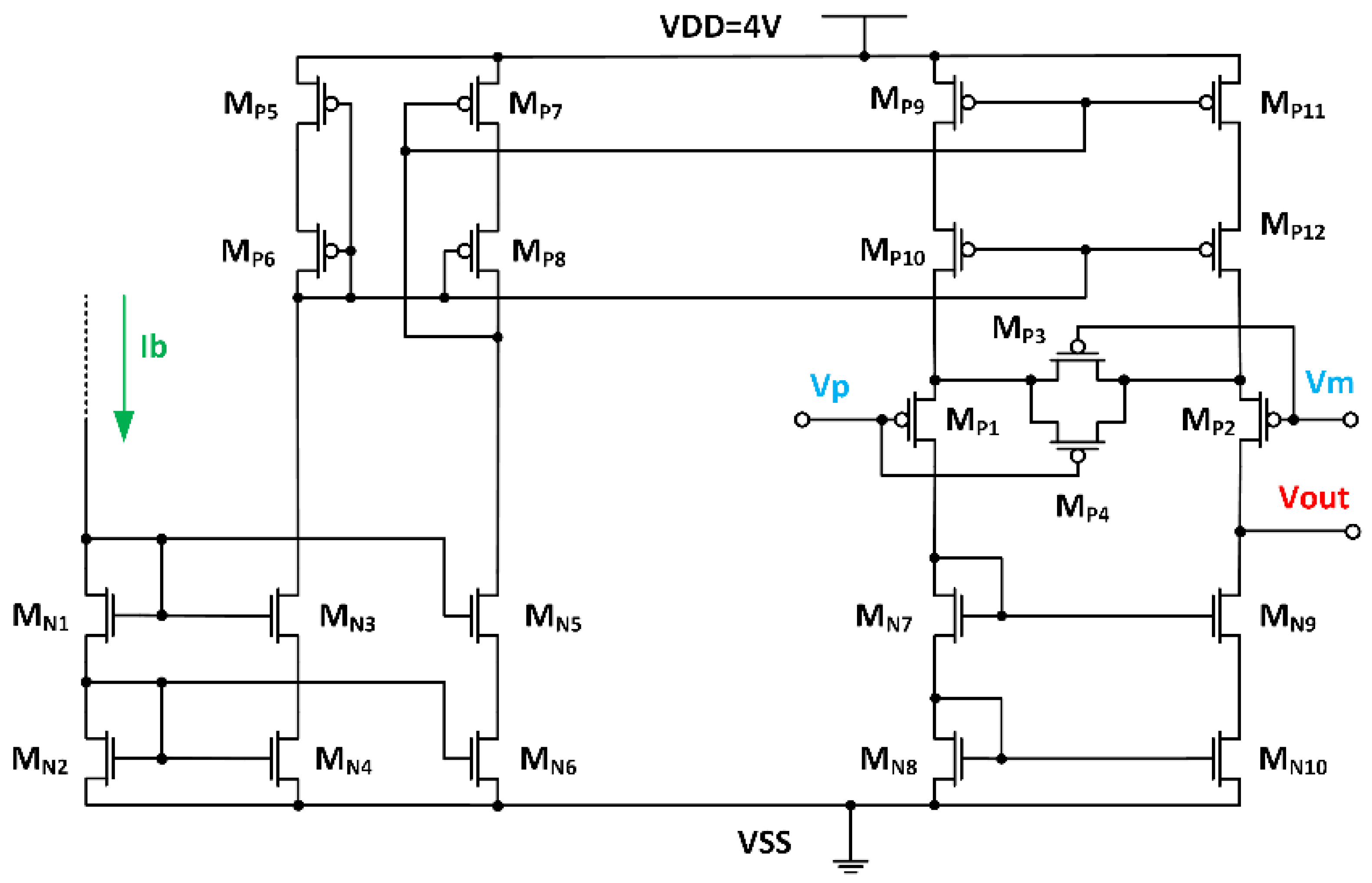
Figure 13, realises the low gm values and therefore has a PMOS input diff pair.
For hand calculations, we have extracted the parameters of the AMS 0.35 μm technology: for NMOS, K’n = μnCox = 117 [μA/V2], VTn = 0.507 [V], and λn = 0.05 [V−1], and for PMOS, K’p = μpCox = −42 [μA/V2], VTp = −0.697 [V], and λn = −0.08 [V−1].
We distinguish between three steps in the design of a single-stage OTA for our application:
(1)
In the case of the input transistors MN1 and MN2 in the input differential pair, we use:
W L 1 , 2 = g m n 1 , 2 2 2 K I D = g m n 1 , 2 2 2 μ C o x I D .
For the degeneration transistors MN3 and MN4 (which operate in the triode region) in the input differential pair, we then have:
W L 3 , 4 = 1 N W L 1 , 2 = 1 6.7 W L 1 , 2 .
Here we can also calculate the gate overdrive voltage (or saturation voltage):
V D s a t = 2 I D g m ,
(2)
In the case of transistors in wide swing cascode current mirrors in the sources of the input pair, we start our calculation with a selected (realistic) overdrive voltage VDsat between 100 mV and 200 mV and calculate gm with
g m = 2 I D V D s a t ,
and then the required transistor dimensions follow:
W L = 2 I D K V D s a t 2 = g m 2 2 K I D
(3)
In the case of transistors that form current mirrors in the drains of an input pair (active load), we perform our calculation in the same way as in case 2 and use the same Equations (28) and (29). The only difference that needs to be noted is that the transistors in this case are of opposite polarity than in case 2.
The W/L values, which were calculated with the above design equations and then simulated by Cadence for the OTAs in our circuit, can be found in Table 4, Table 5 and Table 6. We have obtained three groups of OTAs. Tuning for different CPE angles is performed by changing Ibias with all transistors operating safely in saturation. The required bias current Ibias to obtain the required transconductances in Table 3 for different orders α can be found in Table 7. To reduce the spread of Ibias currents, we need to include OTAs with higher transconductances. In the previous publication in [26], where only one type of OTA was used, the ratio of the critical bias current Ibias is between the maximum of 280 μA and the minimum of 0.9 μA and is higher than 300. In our design, where we chose different OTA topologies, the ratio between the maximum and minimum required bias current Ibias is 10, which is a 30-fold improvement. The dimensions of the MOS transistors in OTAs are given below each of the circuits in the tables. The final topology of the realised CPE is shown in Figure 14.
The MOSFET transistors used as nmos cells are NMOS4, which are designed with 4 fingers and 1 multiplier, and the pmos cells used are PMOS4, which are designed with 8 fingers and 1 multiplier from the PRIMLIB library in the AMS C35B4C3 technology. This technology has no defined multipliers, so instead of multipliers, unit transistors must be copied and connected in parallel. To reduce the influence of the process on the mismatch, the input diff pair has been designed for common centroid matching (A B B A/B A A B) and the current mirrors for interdigitation or linear centroid matching (C C B B A A A A B B C C); the current starts in the centre and flows in a line to the left and right.
The capacitors are realised as linear “cpoly” capacitors, whereby C1 is an 8 × 8 array of 64 unit cells with a capacitance of 156.25 fF (12.85 μm × 13.7 μm) and thus forms 10.0 pF. Capacitor C2 is a 25 × 25 array of 256 unit cells with a capacitance of 346.6 fF (19.5 μm × 20.25 μm) and thus forms 216.56 pF.
In our design, we chose the following bias currents Ibias for MOS transistors in OTAs:
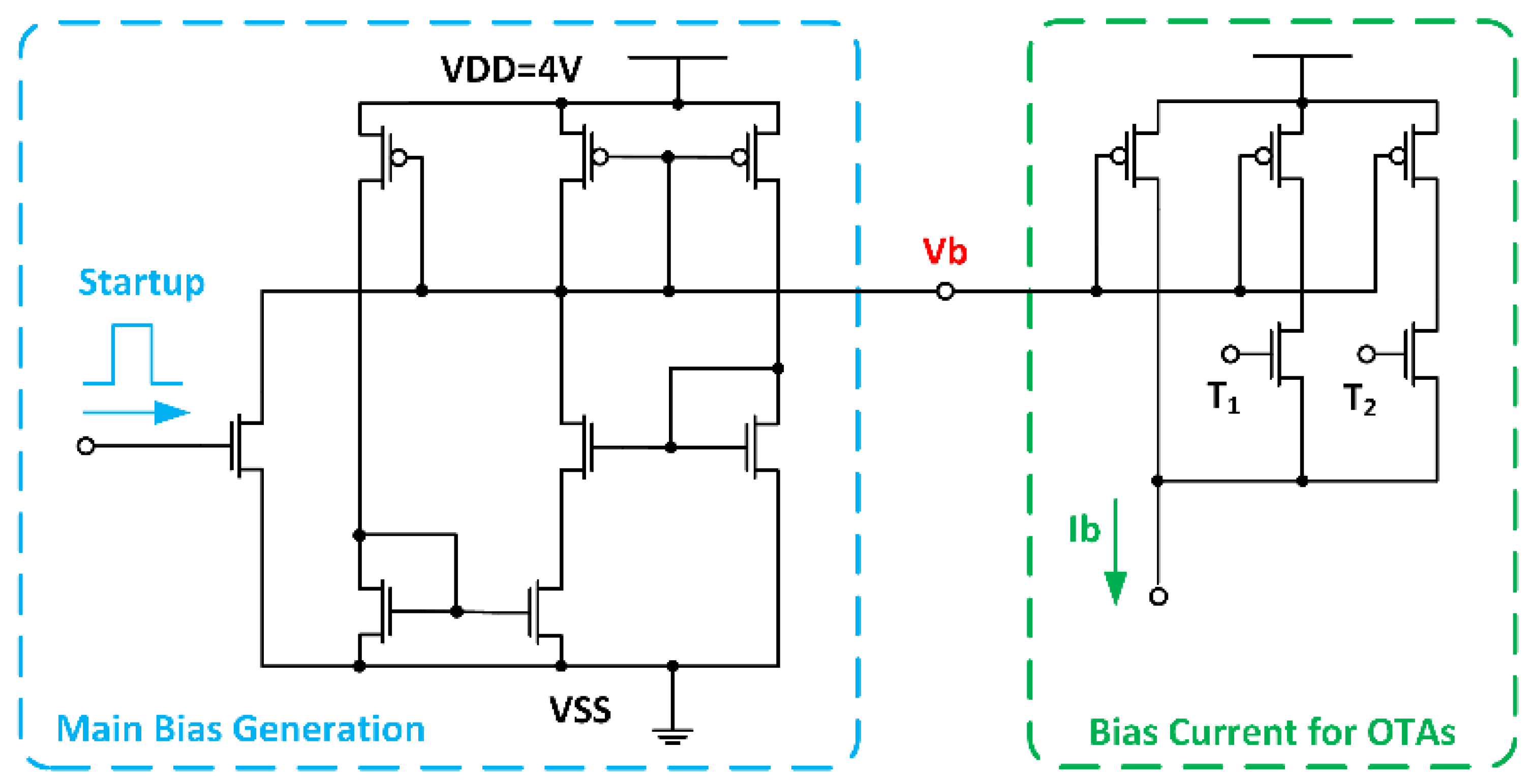
The circuit in Figure 15 is used to provide bias currents. The main bias generation circuit (blue block) is used to generate a stable bias current, which is later mirrored (green block) with a factor suitable for the individual OTAs. Since each OTA needs 3 different currents to implement different phases (30°, 45°, and 60°), the mirroring factor can be digitally controlled with 2 bits (T1 and T2). A manual startup was implemented as a failsafe mechanism to ensure the necessary initial conditions.
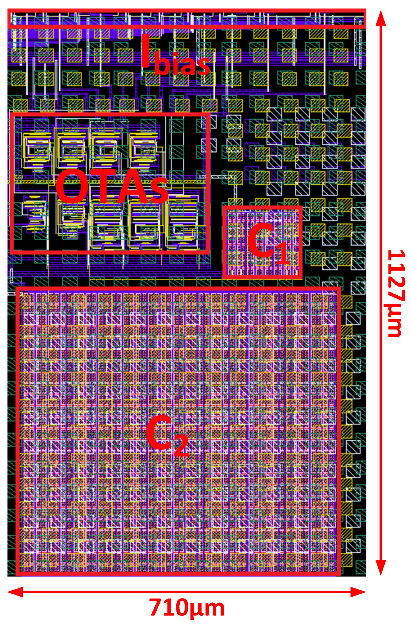
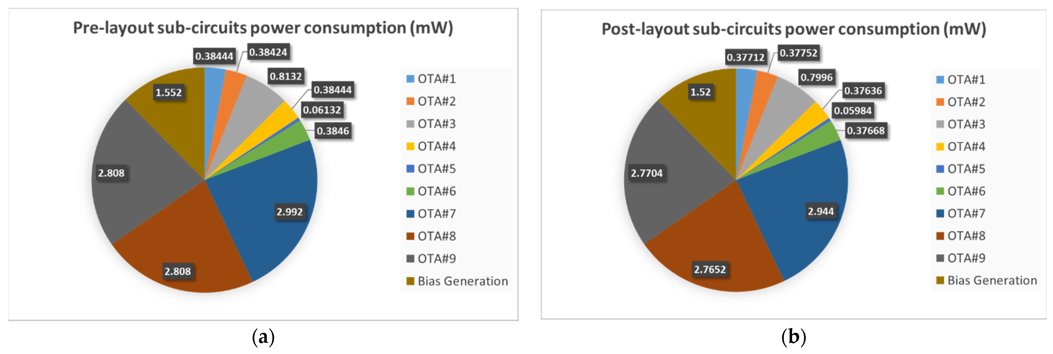
The whole system was implemented in the AMS 350 nm technology node using Cadence Virtuoso tools for the design process. The layout showing the size and location of the subcircuits is presented in Figure 16, indicating a total area of 710 × 1127 µm2. The post-layout study with corresponding simulated results was conducted as a proof of concept, and it is presented in the following Section 4.

3.4. Power Consumption

The power consumption of the entire system is 12.37 mW (12.57 mW pre-layout). Figure 17 shows the power consumption of the individual sub-circuits for pre-layout (Figure 17a) and post-layout (Figure 17b) analysis. For an explanation of the post-layout analysis, see Section 4.
It can be observed that most of the power (together, 68%) is consumed by OTA#7, OTA#8, and OTA#9 (all of type OTA3). The generation of the bias current also consumes a significant part of the power (12%), while the other OTAs together consume the rest (20%). There are slight differences between the results of the pre-layout and post-layout values. The results presented were simulated at the centre frequency (50 kHz) and at an angle of −60°, which is the worst angle for power consumption due to the highest bias currents. Note that the power consumption is slightly lower in the post-layout simulations because some parasitics limit the current spikes drawn from the VDD.

4. Simulated Post-Layout Results

4.1. Setting up the Post-Layout Analysis

The main programme tool used during the design process is Cadence Virtuoso. The first step is to import specific CMOS technology files that contain very accurate models for the desired technology node (AMS 350 nm). The imported models used for MOSFETs and capacitors already have parasitics included in their parameters, which makes them very realistic. Since the models consider the size and shape of the individual elements, even a pre-layout analysis can be quite accurate. The Virtuoso Schematic XL sub-tool is used to create the schematic, and the Virtuoso ADE Assembler sub-tool is used to perform various analyses (Transient, AC, and Monte Carlo). Once the schematic design is finalised and the designer is satisfied with the results of the pre-layout simulation, the layout design can be performed using the Virtuoso Layout XL sub-tool. The physical layout of the circuit includes models of MOSFETs and capacitors as well as the connecting metal lines used as wires. The Assura DRC sub-tool is used to perform the design rule check (DRC) to ensure that all physical elements can be implemented in the desired tech node. The Assura LVS sub-tool performs the Layout-vs-Schematic (LVS) check to ensure that the layout created matches the circuit schematic. Once LVS and DRC are error-free, the parasitics of the metal lines can be extracted with Assura QRC. An additional model of the entire circuit containing all parasitics is automatically created after extraction (the default name is av_extracted). The post-layout simulations were produced with Virtuoso ADE Assembler, but this time the av_extracted model is used instead of the standard schematic.

4.2. AC Analysis

The post-layout (solid) and pre-layout (dashed) results of the AC analysis are demonstrated in Figure 18. Figure 18a shows the magnitude-frequency characteristics of the implemented CPE element for three characteristic angles (−30°, −45°, and −60°). It can be observed that the slope by which magnitude falls with frequency corresponds with the implemented angle. For the classical capacitor, the slope would always be −20 dB per decade. Since the fractional order capacitors are presented, slopes are −6.67 dB, −10 dB, and −13.33 dB per decade for 30°, 45°, and 60°, respectively. The phase-frequency characteristics for three implemented angles are shown in Figure 18b.
A difference between post-layout and pre-layout data can be observed only at higher frequencies due to the additional parasitic capacitors introduced in the form of metal lines that connect elements. The difference between post-layout and pre-layout simulations is not big, as the FOC emulator circuit under consideration is quite simple. Note that demonstrated fractional elements operate as such only within a certain frequency range, which is a result of the approximation.

4.3. Transient Analysis

Figure 19, Figure 20 and Figure 21 present the results of the post-layout transient analysis. For each angle, the circuit was tested with a sine wave of 50 kHz (the central frequency within an operating range) and a 20 mV peak-to-peak amplitude. As expected, the corresponding phase shift between input voltage and input current was observed (−30°, −45°, and −60°). Since the amplitude of the input signal is relatively small and the OTAs used for the approximation are linear in this range, the input current distortion cannot be noticed.
Since the emulator of the CPE is a voltage-excited type, the excitation is defined by the voltage source in the form of an input voltage, and the response is in the form of a current waveform at the same input port as the driving-point impedance under test. Transient analysis in the analogue design environment of the Cadence software ver. IC6.1.7-64b.500.4 enables comprehensive testing and simulation of the operation of the circuit, including all parasitic effects and a large number of parameters in real operation. In contrast to AC analysis, which uses simplified elements in the simulations. The following diagrams are transient simulations from the post-layout analysis of the circuit with extracted parasitics. A look at these diagrams confirms the correct operation of the circuit and the correct phase shift of the current at the input in response to the excitation in the form of a voltage at the same input terminal.

4.4. PVT Corner Analysis

The PVT corner analysis was conducted for the extreme cases in the process (ss, ff, sf, fs), temperature (−10 °C and 110 °C), and supply voltage (3.5 V and 4.5 V). The resulting magnitude-frequency and phase-frequency characteristics for the implemented angles are shown in Figure 22, Figure 23, Figure 24, Figure 25, Figure 26 and Figure 27. It can be observed that the dispersion of the characteristics is lower as the angle is closer to 90°, i.e., a classical capacitor. Further investigation showed that the supply voltage has very little effect on the characteristics, so the main contributing factors to the dispersion are the process and temperature.

4.5. Monte Carlo Analysis

As additional verification, the Monte Carlo (MC) analysis for process and mismatch combined was conducted (100 samples for each angle). As a result, histograms showing variations in average phase shifts are presented in Figure 28, Figure 29 and Figure 30. The MC results also indicate greater variations as the angle is further away from 90°. Observed standard deviations are 2.696°, 2.083°, and 1.425° for angles of 30°, 45°, and 60°, respectively.

5. Conclusions

In this paper, we present the design of a constant-phase element realised with active elements such as OTAs and grounded capacitors. The OTAs are designed in a linearised version with all transistors in strong inversion. This approach is suitable for operation at high frequencies. The phase is tunable by changing the bias currents for each OTA. The digital tuning scheme has been proposed for the first time. There are various one-stage OTAs in use that achieve a very reasonable ratio between bias-current Ibias values, with a maximum ratio of 10. The results of the post-layout simulation in Cadene confirm the feasibility and functionality of the proposed approach. In previous works, authors have developed OTA-C CPE with sub-threshold MOSFETs. Therefore, our contribution is to investigate OTA-C CPE with MOSFETs in strong inversion, operating at high frequencies, and digitally controlled, which has been successfully demonstrated.
The future research topic is the construction of electronically controlled OTA-C constant-phase elements in which a large number of parameters can be controlled: centre frequency, impedance, and element order in fine steps. The design of digitally controllable FOEs (implementing both CPE and FOI in all four quadrants) operating at high frequencies and increasing the approximation order to higher than two is also a future research topic.

Author Contributions

Conceptualization, D.J. and C.P.; methodology, E.E. and M.V.; validation, E.E. and M.V.; formal analysis, E.E.; investigation, E.E.; writing—original draft preparation, E.E., D.J. and M.V.; writing—review and editing, E.E., D.J. and C.P.; project administration, D.J. and C.P. All authors have read and agreed to the published version of the manuscript.

Funding

This research received no external funding.

Data Availability Statement

Data are contained within the article.

Conflicts of Interest

The authors declare no conflicts of interest.

References

  1. Ortigueira, M. An introduction to the fractional continuous-time linear systems: The 21st century systems. IEEE Circuits Syst. Mag. 2008, 8, 19–26. [Google Scholar] [CrossRef]
  2. Elwakil, A. Fractional-order circuits and systems: An emerging interdisciplinary research area. IEEE Circuits Syst. Mag. 2010, 10, 40–50. [Google Scholar] [CrossRef]
  3. Langhammer, L.; Dvorak, J.; Sotner, R.; Jerabek, J.; Bertsias, P. Reconnection–less reconfigurable low–pass filtering topology suitable for higher–order fractional–order design. J. Adv. Res. 2020, 25, 257–274. [Google Scholar] [CrossRef] [PubMed]
  4. Tasneem, S.; Ranjan, R.K.; Paul, S.K.; Herencsar, N. Power-Efficient Electronically Tunable Fractional-Order Filter. Fractal Fract. 2023, 8, 31. [Google Scholar] [CrossRef]
  5. Tsikritsi, E.; Kapoulea, S.; Psychalinos, C. Implementation of the Fractional-Order Model of the Biceps Tissue during Fatigue Exercise. In Proceedings of the 2020 43rd International Conference on Telecommunications and Signal Processing (TSP), Milan, Italy, 7–9 July 2020; pp. 496–499. [Google Scholar] [CrossRef]
  6. Freeborn, T.J. A survey of fractional-order circuit models for biology and biomedicine. IEEE J. Emerg. Sel. Top. Circuits Syst. 2013, 3, 416–424. [Google Scholar] [CrossRef]
  7. Cabrera-Lopez, J.J.; Velasco-Medina, J. Structured Approach and Impedance Spectroscopy Microsystem for Fractional-Order Electrical Characterization of Vegetable Tissues. IEEE Trans. Instrum. Meas. 2020, 69, 469–478. [Google Scholar] [CrossRef]
  8. Wei, Z.; Zhang, B.; Jiang, Y. Analysis and Modeling of Fractional-Order Buck Converter Based on Riemann-Liouville Derivative. IEEE Access 2019, 7, 162768–162777. [Google Scholar] [CrossRef]
  9. Dimeas, I.; Petras, I.; Psychalinos, C. New analog implementation technique for fractional-order controller: A DC motor control. AEU-Int. J. Electron. Commun. 2017, 78, 192–200. [Google Scholar] [CrossRef]
  10. Prasad, R.; Kothari, K.; Mehta, U. Flexible fractional supercapacitor model analyzed in time domain. IEEE Access 2019, 7, 122626–122633. [Google Scholar] [CrossRef]
  11. Tian, J.; Xiong, R.; Shen, W.; Wang, J. A Comparative Study of Fractional Order Models on State of Charge Estimation for Lithium Ion Batteries. Chin. J. Mech. Eng. (Engl. Ed.) 2020, 33, 51. [Google Scholar] [CrossRef]
  12. Mishra, S.K.; Gupta, M.; Upadhyay, D.K. Active realization of fractional order Butterworth lowpass filter using DVCC. J. King Saud Univ.-Eng. Sci. 2020, 32, 158–165. [Google Scholar] [CrossRef]
  13. Jesus, I.S.; Tenreiro MacHado, J.A. Development of fractional order capacitors based on electrolyte processes. Nonlinear Dyn. 2009, 56, 45–55. [Google Scholar] [CrossRef]
  14. Westerlund, S.; Ekstam, L. Capacitor theory. IEEE Trans. Dielectr. Electr. Insul. 1994, 1, 970–973. [Google Scholar] [CrossRef]
  15. Westerlund, S. Dead matter has memory. Phys. Scr. 1991, 43, 174–179. [Google Scholar] [CrossRef]
  16. Liao, X.; Ran, M.; Yu, D.; Lin, D.; Yang, R. Chaos analysis of Buck converter with non-singular fractional derivative. Chaos Solitons Fractals 2022, 156, 111794. [Google Scholar] [CrossRef]
  17. Shah, Z.M.; Kathjoo, M.Y.; Khanday, F.A.; Biswas, K.; Psychalinos, C. A survey of single and multi-component fractional-order elements (FOEs) and their applications. Microelectron. J. 2019, 84, 9–25. [Google Scholar] [CrossRef]
  18. Cisse Haba, T.; Ablart, G.; Camps, T.; Olivie, F. Influence of the electrical parameters on the input impedance of a fractal structure realised on silicon. Chaos Solitons Fractals 2005, 24, 479–490. [Google Scholar] [CrossRef]
  19. Biswas, K.; Sen, S.; Dutta, P.K. Realization of a constant phase element and its performance study in a differentiator circuit. IEEE Trans. Circuits Syst. II Express Briefs 2006, 53, 802–806. [Google Scholar] [CrossRef]
  20. Adhikary, A.; Shil, A.; Biswas, K. Realization of Foster structure-based ladder fractor with phase band specification. Circuits Syst. Signal Process. 2020, 39, 2272–2292. [Google Scholar] [CrossRef]
  21. Tsirimokou, G.; Psychalinos, C.; Elwakil, A.S. Fractional-order electronically controlled generalized filters. Int. J. Circuit Theory Appl. 2017, 45, 595–612. [Google Scholar] [CrossRef]
  22. Tsirimokou, G.; Psychalinos, C.; Elwakil, A. Design of CMOS Analog Integrated Fractional-Order Circuits; Springer International Publishing AG: Cham, Switzerland, 2017; ISBN 978-3-319-55632-1. [Google Scholar]
  23. Tsirimokou, G.; Psychalinos, C.; Elwakil, A.S.; Salama, K.N. Electronically tunable fully integrated fractional-order resonator. IEEE Trans. Circuits Syst. II Express Briefs 2018, 65, 166–170. [Google Scholar] [CrossRef]
  24. Kuo, K.C.; Leuciuc, A. A linear MOS transconductor using source degeneration and adaptive biasing. IEEE Trans. Circuits Syst. II Analog. Digit. Signal Process. 2001, 48, 937–943. [Google Scholar] [CrossRef] [PubMed]
  25. Elamien, M.B.; Mahmoud, S.A. A Linear CMOS balanced output transconductor using double differential pair with source degeneration and adaptive biasing. In Proceedings of the 2016 IEEE 59th International Midwest Symposium on Circuits and Systems (MWSCAS), Abu Dhabi, United Arab Emirates, 16–19 October 2016; pp. 16–19. [Google Scholar] [CrossRef]
  26. Kostelac, F.; Coza, A.; Jurisic, D. Fractional-Order Elements Using Tunable OTA-C Structures. In Proceedings of the 2021 44th International Convention on Information, Communication and Electronic Technology (MIPRO), Opatija, Croatia, 27 September–1 October 2021; pp. 119–124. [Google Scholar] [CrossRef]
  27. Mijat, N.; Jurisic, D.; Moschytz, G.S. Analog Modeling of Fractional-Order Elements: A Classical Circuit Theory Approach. IEEE Access 2021, 9, 110309–110331. [Google Scholar] [CrossRef]
  28. Jurisic, D.; Mijat, N.; Moschytz, G. MATLAB Code for Calculating the Minimax Immitance for Approximating Fractional-Order Elements. Available online: https://www.mathworks.com/matlabcentral/fileexchange/96762-fractional-order-elements-foes-using-minimax-approximation (accessed on 20 April 2024).
  29. Krishna, B.T. Studies on fractional order differentiators and integrators: A survey. Signal Process. 2011, 91, 386–426. [Google Scholar] [CrossRef]
  30. Mason, S. Feedback Theory-Some Properties of Signal Flow Graphs. Proc. IRE 1953, 41, 1144–1156. [Google Scholar] [CrossRef]
  31. Mason, S. Feedback Theory-Further Properties of Signal Flow Graphs. Proc. IRE 1956, 44, 920–926. [Google Scholar] [CrossRef]
  32. Razavi, B. Design of Analog CMOS Integrated Circuits, 2nd ed.; McGraw-Hill: New York, NY, USA, 2017; ISBN 9780072524932. [Google Scholar]
  33. Carusone, T.C.; Johns, D.; Martin, K. Analog Integrated Circuits Design; John Wiley & Sons: Hoboken, NJ, USA, 2012; ISBN 9780470770108. [Google Scholar]
  34. Sansen, W. Analog Design Essentials; Springer: Berlin/Heidelberg, Germany, 2006; ISBN 9780387257464. [Google Scholar]
Figure 1. (a) Magnitude- and (b) phase-frequency characteristics of normalised ideal CPE for α = −1/3 (−30°), −1/2 (−45°), and −2/3 (−60°).
Electronics 13 02066 g001
Figure 2. OTA-C implementation of a voltage-excited reconfigurable IFLF structure of an integrator/differentiator with asymmetric input.
Electronics 13 02066 g002
Figure 3. Emulator for the realisation of the voltage-excited grounded impedance from the transfer function H(s) [22].
Electronics 13 02066 g003
Figure 4. OTA-C implementation of a voltage-excited reconfigurable IFLF structure of an integrator/differentiator with differential input.
Electronics 13 02066 g004
Figure 5. Emulator for the realisation of the voltage-excited floating input impedance from the transfer function H(s) [22].
Electronics 13 02066 g005
Figure 6. Signal-flow graph of the second-order IFLF structure for the voltage-excited floating FO capacitor/inductor.
Electronics 13 02066 g006
Figure 7. Signal-flow graph of the second-order IFLF structure in the final version with voltage nodes.
Electronics 13 02066 g007
Figure 8. IFLF structure with emulation scheme for the voltage-excited floating FO capacitor with maximum number of OTAs and transconductance value gm2. The OTAs are labelled from OTA#1 to OTA#8, where #1–#8 stands for number 1 to number 8.
Electronics 13 02066 g008
Figure 9. (a) Normalised amplitude-frequency (in dB) and (b) phase-frequency (in °) characteristics of 1/H(s), where H(s) is defined by CFE and MMX for α = 1/3 (30°), 1/2 (45°), and 2/3 (60°). Detailed analysis for the case H(s) with α = 1/2 (45°): (c) zoomed amplitude-frequency and (d) phase-frequency response comparison; (e) absolute amplitude error; and (f) absolute phase error.
Electronics 13 02066 g009
Figure 10. (a) Magnitude- and (b) phase-frequency characteristics simulation of the FOE impedance Z(s) for circuits in Table 2 and Table 3.
Electronics 13 02066 g010
Figure 11. OTA1 and OTA2 schematic.
Electronics 13 02066 g011
Figure 12. OTA3 schematic.
Electronics 13 02066 g012
Figure 13. OTA4 schematic.
Electronics 13 02066 g013
Figure 14. Final OTA-C emulation scheme for the voltage-excited floating FO capacitor. The OTAs are labelled from OTA#1 to OTA#9, where #1–#9 stands for number 1 to number 9.
Electronics 13 02066 g014
Figure 15. Bias current generation.
Electronics 13 02066 g015
Figure 16. Layout.
Figure 16. Layout.
Electronics 13 02066 g016
Figure 17. Power consumption of the individual sub-circuits. (a) Pre-layout. (b) Post-layout.
Electronics 13 02066 g017
Figure 18. (a) Magnitude- and (b) phase-frequency characteristics (φ = −30°, −45°, −60°). The dashed lines represent the pre-layout analysis, while the solid lines represent the post-layout analysis.
Electronics 13 02066 g018
Figure 19. Transient analysis (φ = −30°).
Electronics 13 02066 g019
Figure 20. Transient analysis (φ = −45°).
Electronics 13 02066 g020
Figure 21. Transient analysis (φ = −60°).
Electronics 13 02066 g021
Figure 22. Magnitude-frequency characteristics (φ = −30°).
Electronics 13 02066 g022
Figure 23. Phase-frequency characteristics (φ = −30°).
Electronics 13 02066 g023
Figure 24. Magnitude-frequency characteristics (φ = −45°).
Electronics 13 02066 g024
Figure 25. Phase-frequency characteristics (φ = −45°).
Electronics 13 02066 g025
Figure 26. Magnitude-frequency characteristics (φ = −60°).
Electronics 13 02066 g026
Figure 27. Phase-frequency characteristics (φ = −60°).
Electronics 13 02066 g027
Figure 28. MC variations due to process and mismatch (φ = −30°).
Electronics 13 02066 g028
Figure 29. MC variations due to process and mismatch (φ = −45°).
Electronics 13 02066 g029
Figure 30. MC variations due to process and mismatch (φ = −60°).
Electronics 13 02066 g030
Table 1. Second-order CFE and MMX approximations for three positive α values and normalised frequency ω0 = 1.
α (φ°)CFEMMX
1/3 (30°) 2.8 s 2 + 7 s + 1 s 2 + 7 s + 2.8 2.83673 s 2 + 7.45924 s + 1 s 2 + 7.45924 s + 2.83673
1/2 (45°) 5 s 2 + 10 s + 1 s 2 + 10 s + 5 5.03262 s 2 + 10.4397 s + 1 s 2 + 10.4397 s + 5.03262
2/3 (60°) 10 s 2 + 16 s + 1 s 2 + 16 s + 10 9.85595 s 2 + 16.1252 s + 1 s 2 + 16.1252 s + 9.85595
Table 2. Second-order MMX approximation (C = 500 pF @ 50 kHz) τi and Gi.
α (φ°)−1/3 (−30°)−1/2 (−45°)−2/3 (−60°)
τ10.426732 μs0.304902 μs0.1974 μs
τ28.37003 μs6.60306 μs5.208 μs
G22.836735.032629.85595
G1111
G00.3525190.1987040.10146
Table 3. Second-order MMX approximation (C = 500 pF @ 50 kHz) gmi and Ci.
α (φ°)OTA−1/3 (−30°)−1/2 (−45°)−2/3 (−60°)
gm1#323.434 μS32.7974 μS50.659 μS
gm2#1, 2, 425.874 μS32.7974 μS41.584 μS
G0gm2#59.1209 μS6.51696 μS4.219 μS
G1gm2#625.874 μS32.7974 μS41.584 μS
G2gm2#773.39 μS165.057 μS409.85 μS
gm, V/I#8157.08 μS157.08 μS157.08 μS
C1-10 pF10 pF10 pF
C2-216.56 pF216.56 pF216.56 pF
pseudo-cap. Cα2.31 uF/s0.67280.25 nF/s0.534.0 nF/s0.33
Table 4. MOSFET transistor dimensions of OTA1 and OTA2 (NMOS INPUT).
MOSFETAspect Ratio OTA-1Aspect Ratio OTA-2
MP1–MP1020 μm/1 μm20 μm/1 μm
MN1–MN214.4 μm/2 μm9 μm/2 μm
MN3–MN42.1 μm/2 μm1.4 μm/2 μm
MN92 μm/1 μm2 μm/1 μm
MN5–MN8, MN10–MN1610 μm/1 μm10 μm/1 μm
Table 5. MOSFET transistor dimensions of OTA3 (NMOS INPUT).
MOSFETAspect Ratio OTA-3
MP1–MP2, MP13–MP14100 μm/1 μm
MP3–MP1220 μm/1 μm
MN1–MN220 μm/2 μm
MN3–MN43 μm/2 μm
MN5–MN6, MN19–MN2050 μm/1 μm
MN122 μm/1 μm
MN7–MN11, MN13–MN1810 μm/1 μm
Table 6. MOSFET transistor dimensions of OTA4 (PMOS INPUT).
MOSFETAspect Ratio OTA-4
MP1–MP23 μm/2 μm
MP3–MP41 μm/4.5 μm
MP54 μm/1 μm
MP6–MP1220 μm/1 μm
MN1–MN1010 μm/1 μm
Table 7. Table of bias currents.
α (φ°)OTA−1/3 (−30°)−1/2 (−45°)−2/3 (−60°)
I01#3 (OTA2)4.6 μA8.0 μA17.4 μA
I02#1, 2, 4 (OTA1)4 μA5.6 μA8 μA
G0 I02#5 a (OTA4)7.2 μA4 μA2 μA (descending)
G1 I02#6 (OTA1)4 μA5.6 μA8 μA
G2 I02#7 b (OTA3)1.7 μA5 μA21.4 μA
I0, V/I#8, 9 (2× OTA3)1 μA1 μA1 μA
a For OTA #5, which has low transconductance values, we used the OTA with a PMOS input pair. b For OTA #7, which has high transconductance values, we used the current multiplier ×5.
Disclaimer/Publisher’s Note: The statements, opinions and data contained in all publications are solely those of the individual author(s) and contributor(s) and not of MDPI and/or the editor(s). MDPI and/or the editor(s) disclaim responsibility for any injury to people or property resulting from any ideas, methods, instructions or products referred to in the content.

