1. Introduction
Time-critical applications like medical devices, personal smart drones, autonomous vehicles, robots, industrial IoT, control systems, etc., need to be operated with delay- and power-optimized mechanisms. One of the best methods for lowering the delay, power, and energy use of digital integrated circuits (ICs) is supply voltage scaling [
1,
2]. In order to achieve the lowest energy consumption or the maximum energy efficiency, designs have been scaled to the sub-/near-threshold voltage range by edge devices [
3,
4,
5,
6]. These self-sufficient gadgets even lower the supply voltage below 100 mV, as they rely on environmental energy scavenging [
7]. Lowering supply voltages, however, might cause timing issues such as fractions and malfunctions in voltage-sensitive components like analog blocks and SRAM arrays. Therefore, for complicated System-on-Chips and application-specific integrated circuits, many power domains must be employed. Some of these power domains have a dynamic power source originating from the voltage at a nominal to sub threshold range, while others are operating at very low voltage or near-nominal voltage regions. To ensure stable connectivity inpower domains between high voltage (VDDH) and low voltage (VDDL) modules, the LSs are mostly wanted for level translation at various voltages in a multi-supply voltage system. Simple CMOS buffers driven by VDDL can handle high-to-low conversions, but additional design work is needed to achieve low-to-high LSs with the least amount of time, power, and area. The literature report describes a wide range of LSs [
8,
9,
10,
11,
12,
13,
14,
15,
16].
These LSs are often built using one of the two varieties of traditional LS topologies: the current mirror LS (CMLS) or cross-coupled LS (CCLS). Unfortunately, the CCLS has a significant problem with current contention, which causes the level change to take longer and the current consumption to increase. On the other hand, the CMLS often has a high static current, which results in considerable power overhead. This paper proposes a hybrid LS named the full-swing nanosecond delay hybrid level shifter (FDLS), for ultra-wide range and full swing for time critical applications. It combines the advantages of the topologies of CCLS and CMLS with a swing-aware output inverter. Two CMLS stages are used to dynamically modify the CCLS stage’s pull-up strength. Fast and ultra-wide-range level shifting is ensured by the great mitigation of contention currents seen in traditional CCLS. The suggested FDLS demonstrates the best delay and full swing among state-of-the-art LSs, according to both the measurement findings and simulation results. In comparison to the state-of-the-art LSs, the FDLS also exhibits contrasting minimum convertible input levels, propagation delays, transition energy usages, leakage power consumptions, and layout space. Additionally, the suggested FDLS exhibits strong supply voltage scaling and delay scalability [
17,
18,
19,
20].
Usually, two cross-coupled inverters make up the cross-coupled LS. One of the inverters receives the input, while the other receives the output. The current mirror LS works by producing an output voltage that matches the intended level shift by reflecting the current from a reference circuit.
Different applications can use the varied benefits offered by both CCLS and CMLSs, contingent upon the particular needs of the integrated circuit design. Current mirror LSs are distinguished by their accuracy and versatility, but cross-coupled LSs are preferred for their simplicity and quickness. These kinds of creative level-shifting approaches will surely become increasingly more important in the world of semiconductor design and manufacturing, as the need for more complicated and energy-efficient ICs grows.
The review on previously released LSs is examined and debated in
Section 2. In
Section 3, the proposed FDLS is shown. Evaluation of the proposed LS is provided in
Section 4 for the assessment of different LSs.
Section 5 presents the conclusion of the article.
2. Literature Survey
The previously reported LSs, modified versions of the CMLS, and the traditional CCLS are discussed in this chapter. The advantages and disadvantages of released LSs are examined and contrasted. Using complementary pull-down and pull-up networks, CCLS is able to achieve nearly 5% standby power compared with the basic LS. On the other hand, substantial current conflict occurs in the CCLS during high-to-low and low-to-high transitions. To initiate the switching, the powerful pull up network (PUN) driven by VDDH must be defeated by the pull down network (PDN) driven by VDDL. When VDDL decreases, it causes a sharp rise in delay and energy consumption, and when VDDL reaches the sub threshold area, it even causes malfunctions. Larger pull-down transistors or low-threshold voltage transistors can help with this problem, but larger devices will always require more space and energy during transitions, and low threshold voltage transistors will always result in greater leakage current [
8].
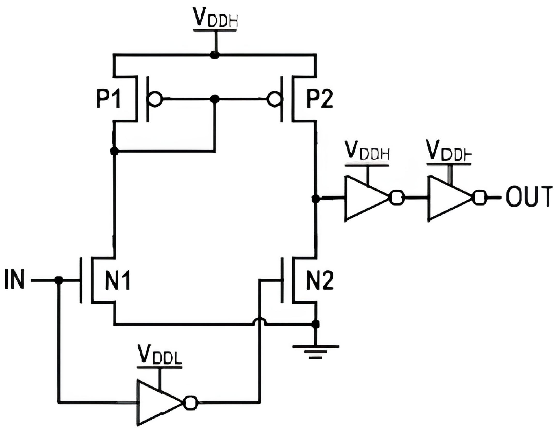
Figure 1 depicts the topology of the traditional CMLS, which does away with the existing CCLS contention problem. However, while IN stays at logic “1”, the CMLS experiences a significant static current.
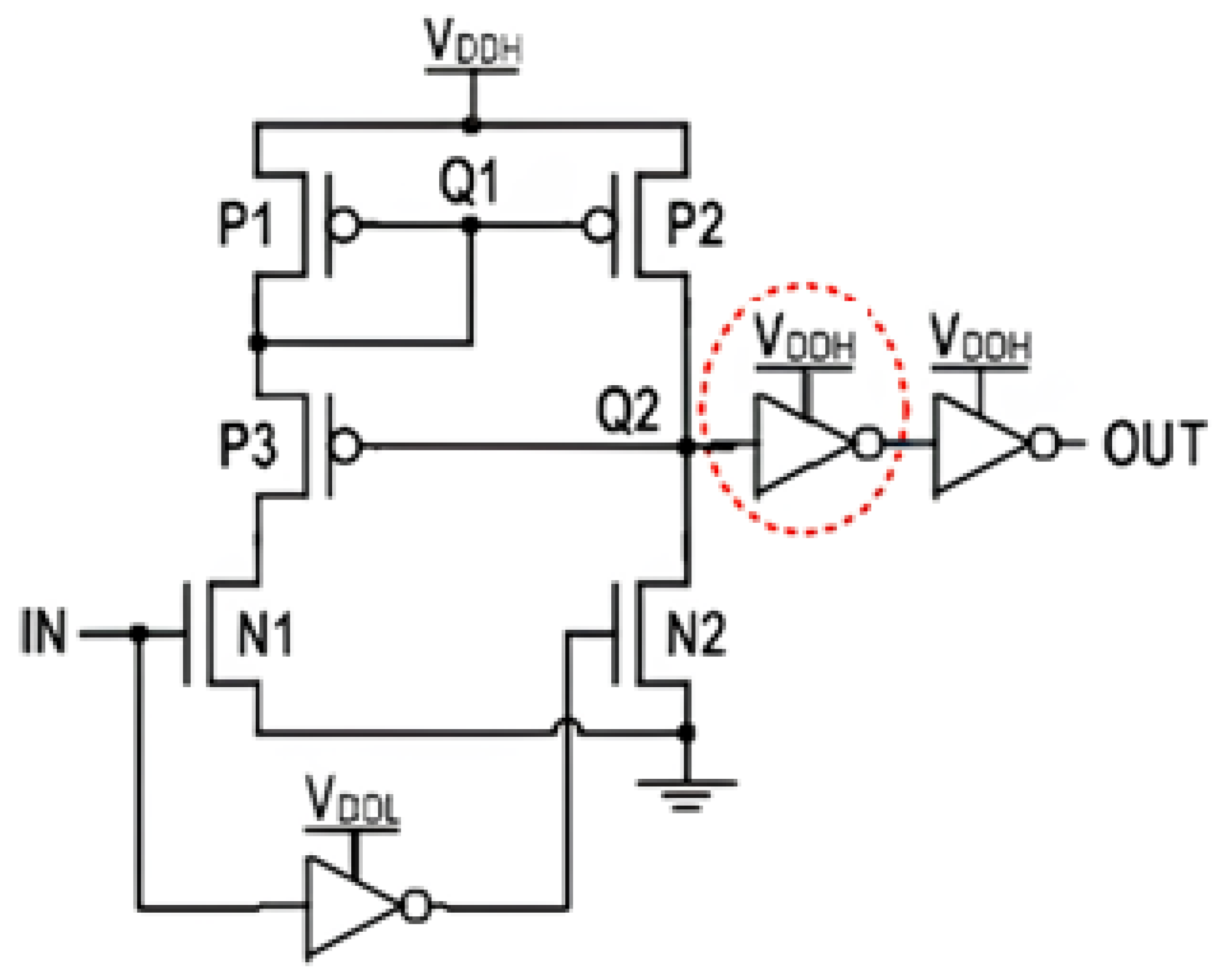
Figure 2 displays the Wilson CMLS (WCMLS), a modified CMLS [
10]. Inserting a feedback MOS transistor P3 closes the stagnant current route. On the other hand, the 0.2 V to 1.2 V transition is slowed down by the cut-off P3, which increases the voltage at node Q1. Moreover, because Q2 cannot be brought up to complete the VDDH, a substantial quantity of constant current flows via the first output side inverter that is attached to Q2 instantly.
The current-limiter CCLS is proposed in [
8,
21,
22]. The inclusion of multi-threshold voltage transistors and the diode-connected current limiter with MOS transistors N3 and N4 cause the pull-up network to help diminish the current contention issue stated above. However, when VDDL and VDDH are close to one another, the delay of the CCLS cannot scale properly because the PUN is perpetually feeble. The CCLS is not suited for voltage scaling applications due to the delay scalability problem.
The pre-amplifier CCLS is presented in [
9], with a pre-amplifier and an output latch constituting its major conversion step. When IN and OUT do not match, the pre-amplifier’s logic-error-correcting circuit produces the complimentary amplified signals. The stage of latching is a full-swing output that is produced from the amplified voltages using a cross-coupled topology. However, the production of intermediate voltage levels is tedious. This results in a significant area overhead, as well as a decrease in the speed at which the levels transition.
In [
11], a diode-chain CMLS is suggested as a solution to the problems of the WCMLS. In order to maintain enough strength in the pull-up, the voltage of the intermediate node is lowered using an input-controlled diode chain. As a result, the diode-chain CMLS achieves static-current-free and full-swing functioning, albeit at the diode chain’s high area cost.
A logic-error-detection-equipped CMLS is proposed in [
12]. Positive feedback provides a full swing of OUT and speeds up OUT transitions via joining the gate to the drain. The logic error detection circuit is where this design flaw is present. A low inversion input voltage level might not be able to fully draw down the action of the driving inverter during high-to-low transitions. Constrained conversion range and high energy use follow from the present dispute between P5 and N3, and if ERR does not grow, between P4 and N2.
The following is a synopsis in the literature review that identifies the desired characteristics of LSs.
Limited-current-contention: High transition energy consumption and a restricted conversion range are the drawbacks of a LS with a strong contention current.
Static-current-free: High static power consumption iscaused by incomplete voltage swings at internal nodes and/or unclamped static current paths.
Speed-limitation-less: Long transition delays are caused by current contention, drive strengths, and transitional voltage fluctuations, particularly at extremely low voltage levels.
Delay scalable: A LS’s delay should ideally go down when the voltage differential between VDDH and VDDL narrows
Area efficient: It is preferable to have a LS with fewer transistors and smaller transistors.
The five qualities listed above are used to assess each of the reviewed LSs and propose theFDLS in the evaluation chapter.
3. Proposed Full-Swing Nanosecond Delay Hybrid Level Shifter
To overcome the issues with static current, speed limitation, current contention, and voltage swing of the previously reported LSs, the new full-swing nanosecond delay hybrid LS structure that combines the benefits of CCLS and CMLS is proposed in this chapter. The full-swing nanosecond delay hybrid level shifter (FDLS) is dominant in terms of delay and energy.
Figure 3 displays its conceptual design. There is one CCLS stage and one CMLS stage in the main conversion circuitry. The operation of the proposed LS is described in two cases:
Figure 4a depicts the processes involved in the 0.20 V to 1.20 V transition and
Figure 4b depicts processes involved in the 1.20 V to 0.20 V transition. The switching factor of the FDLS is low in the order 0.75 to 0.95, influenced by the P5–N6 transistors, which are determined by W and L of the N7 as per Equation (1).
where
is the switching factor,
CL is the capacitive load, VDDH is the level shifter supply voltage, and
fIN is the input level shifting signal frequency.
A short circuit current between VDDH to GND through P5–N6 is controlled by the current-aware device
N7, which has been used here to limit the current under a situation when the OUT node has a swing lesser than the noise margins based on Equation (2).
where
CoxN7 is the oxide layer capacitance of
N7;
WN7 and
LN7 are the widths and length of
N7, respectively; and
VGSN7 and
VDSN7 are the Gate to Source and Drain to Source voltages, respectively, of the
N7 transistor.
VTN7 is the threshold voltage of
N7.
The voltage difference of first-order terms may pilot to the partial value and makes the OUT node voltage a strong zero or VDDH, and driving the output inverter produces a VOUT equal to VDDH, as per mathematical model Equation (3).
where V
P5-N6 is the voltage at the OUT node,
GmP5 is the transconductance of the P5,
VthP5 is the nominal
Vt of the P5,
VthMN6 is the nominal V
t of the N6, and
CL is the load capacitances of the OUT.
To charge NA in the FDLS and discharge the OUT node to GND, the rising current I
RISE is mirrored as I
FALL, the sum of C
L and the rate of transform of VOUT. As a result, rise times and fall times of OUT is made balanced, referring to Equation (4).
To augment the switching feature and ensure a low area for lower VDDL stoutness, a dual VTH logic approach was utilized alongside suitable transistor scaling. Purposely, low Vt devices were used in N2, N3, and N4, and the rest of the devices are regular Vt. The proposed design is bidirectional, and is capable of level-up or level-down.
3.1. Input (IN) Transition from 0.20 V to 1.20 V
Initially, IN is the 0.2 V and node NA is at a low voltage level of VSS. When IN transitions from 0.2 V to 0 V, both transistors N1 and N2 turn OFF, pulling the NC up and generating a current in P2. This mirror current through transistor P2 discharges NB down. While NB is discharged and the drive strength of transistor P3 turns out to be stronger and turned OFF, transistors N3 and N5 make transistor P5 OFF, and the down NA makes the transistor N6 ON lead to OUT equal to VSS through the discharging of transistor N6. Transistor N3 thus easily pulls the NA up with no issues from P3. In this case, the current contention issue is substantially mitigated with the aid transistors P3 and N5.
3.2. Input (IN) Transition from 1.20 V to 0.20 V
Initially, IN is 0 V, the MOS transistor N3 is in an OFF state, and node NA would be at a high voltage level of VDDH. When input IN transitions from 0 V to 0.2 V, both transistors labeled N1 and N2 turn ON, which pulls NC down, in turn generating the current in P2. The current through transistor P2 makes NB charge up. When NB is charged-up, and the drive strength of transistor P3 turns out to be weaker and turned ON, transistors N3 and N5 make transistor P5 ON, and the down NA makes the transistor N6 OFF. This leads to OUT being equal to VDDH through the charging of transistor P5. By leveraging the current mirror current, the current conflict between P3 and N5 was significantly concealed. Transistor N3 thereby pulls NA down without too much difficulty from P3. The current contention issue is substantially mitigated with the aid transistors P3 and N5.
The transistor N4 acts as a pass transistor to facilitate a static-current-free path between the VDDH and VSS through P4 and N3, maintaining sufficient pull-up and pull-down strengths between the arms of transistors P3 and P4. The intermediate voltage generation between NA and NB leads to a reduction in transition delays, especially when IN is at an ultra-low voltage level. The transistor N7 will act as short circuit protection between P5 and N6 withan inversion voltage between 0 V and 1.20 V of OUT.
4. Evaluation of Full-Swing Nanosecond Delay Hybrid Level Shifter
The proposed hybrid FDLS is analyzed using the cadence virtuoso tool for post-layout simulation in 45-nm CMOS technology. The suggested hybrid LS may convert input levels as low as 100 mV. Various metal layers are employed in this circuit to avoid overlap of metal connections.
Figure 5 depicts the layout of proposed FDLS. The area of the FDLS is 9.5 μm
2 and 13.5 μm
2 in the 45-nm technology. In the layout of circuits in 45 nm CMOS, the W/L size of almost all MOS devices are set to 90 nm/45 nm to reduce parasitic capacitances. Furthermore, LVT devices were used for N2, N3, and N4, and rests of the devices are regular Vt. It can be noticeable that in order to decrease the parasitic capacitance and size of P3, it has been put in the n-well, and body terminals of P1–P4 were tied to VDDH. In order to make delay low, both IN and OUT inverters are simulatedin another test node, as depicted in
Figure 3. This makes the delay between IN and OUT extremely low.
At 27 °C (room temperature), the suggested LS could provide voltage conversation from 0.20 V to 1.20 V at 1MHz input frequency. The input low voltage supply is operated with 0.2 V. The level up conversion simulation waveform is shown in
Figure 6. It is observed that in the hybrid CMOS level up shifter, the voltage level converts from 0.20 V to 1.20 V. The overall power consumption of the LS is 3.81 µW, the propagation delay is 8.38 ns, and the power delay product is 31.92 fWs, which is far better than the LSs of [
23,
24].
4.1. Robustness against Temperature Variations
A comparison on average power and propagation delay was performed by varying temperature from −50 °C to 30 °C at constant voltages VDDL = 0.20 V and VDDH = 1.20 V. The proposed LS has transition delays for 0.20 V to 1.20 V voltage conversion throughout a temperature range. The suggested FDLS has the least amount of delay fluctuation, indicating that the design is resilient to changes in temperature, and displays the transition delays for 0.20 V to 1.20 V level conversions throughout a temperature range. The suggested FDLS has the least amount of delay fluctuation, indicating that the design is resilient to changes in temperature. There is no effect on average power, energy consumption, and propagation delay by varying temperature from −50 °C to 30 °C at constant voltages VDDL = 0.20 V and VDDH = 1.20 V.
A comparison on energy and delay by varying temperature from −50 °C to 30 °C at constant voltages VDDL = 0.20 V and VDDH = 1.20 V is shown in
Figure 7. It displays the transition delays for a 0.20 V to 1.20 V level conversion throughout a temperature range. The least amount of delay variation is displayed by the suggested FDLS, which substantiates the robustness of FDLS design against the disparity in temperature. The suggested FDLS has the least amount of delay fluctuation, indicating that the design is resilient to changes in temperature. In order to ascertain the mean power and energy use of a circuit or apparatus at specified supply voltages of VDDL = 0.20 V and VDDH = 1.20 V at a certain temperature, we want a more comprehensive understanding of the circuit’s properties or a particular model to utilize.
4.2. Delay as a Function of Bias Voltages
The measured propagation delay versus VDDH varies from 1.0 V to 1.20 V at different constant VDDH values, and are 0.20 V, 0.30 V, and 0.40 V. A number of factors affect propagation delay in digital circuits, and one of them is the high-level supply voltage shown in
Figure 8. Propagation delay in general is the amount of time it takes for a digital circuit’s output to change in reaction to an alteration in its input. The amount of time that passes before a change in the input signal is reflected by a comparable change in the output signal is known as the propagation delay. Conversely, VDDH denotes the high-level power supply voltage in CMOS logic, specifying the voltage level at which the circuit functions when the logic high (1) is reached at the output. Propagation delay and supply voltage VDDH often have an inverse relationship: the propagation delay tends to decrease as the VDDH increases.
The measured propagation delay versus VDDL varies from 0.20 V to 0.40 V at different constant VDDL values, and are 1.00, 1.10, and 1.20. The low-level supply voltage in digital circuits can also have an impact on the propagation delay. An equation akin to the one for VDDH may be used to explain the link between propagation delays. An equation like the one for VDDH may be used to explain the link between propagation delays shown in
Figure 9.
The characteristics of propagation delay and VDDL are strongly connected while designing digital CMOS circuits. The term “propagation delay” describes the amount of time needed for an alteration in the input signal to result in an equivalent alteration in the output signal. However, it is important to pay attention to the propagation delay as well as VDDL optimization. A reduced VDDL can result in issues such as reduced noise margins, greater sensitivity to noise, and issues with signal integrity, while it can also improve power efficiency by reducing the power consumption. In order to attain the performance desired by circuits, the designers must consider the benefits of the propagation delay and VDDL, considering factors such as the power efficacy, noise margin, and overall reliability.
4.3. Power Consumption as a Function of Bias Voltages
A comparison of average energy consumption, power consumption, and propagation delay was obtained using VDDL from 0.20 V to 0.40 V at a constant voltageVDDH = 1.20 V as well as temperature 27 °C. The effects on energy consumption, power efficiency, and digital circuit performance can be seen by altering the voltage of the supply at low levels of VDDL, which is shown in
Figure 10. While the average power consumption might fall, it can be countered by a rise in leakage currents even at very low voltages, when VDDL falls to its threshold. Propagation latency is increased because of the lower voltage margin to allow for faster transistor switching. On the other hand, higher current levels in transistors lead to more power consumption per unit. The higher VDDL will reduce the latency of propagation. A higher VDDL can result in a lower energy use per operation because of quicker switching, even though overall energy consumption might increase. To achieve the optimal balance between performance, power, and energy efficiency, improving VDDL often entails balancing these trade-offs based on the unique requirements and limits of the application. Often, this is performed by utilizing techniques like dynamic voltage and frequency scaling. In contrast, in CMOS circuits, VDDL stands for low-level power supply voltage, which denotes the voltage level at which the circuit functions while its logic output is low. Propagation delay and VDDL often have a direct connection in which the propagation delay tends to grow as the low-level supply voltage VDDL drops. The reason for this connection is because a lower supply voltage causes the transistors to have less energy available, which slows down the pace at which they flip, and lengthens the propagation delay.
In reference to
Figure 10, digital circuit power consumption is heavily impacted by the high-level supply voltage VDDH. In a CMOS digital circuit, power is usually expressed as a square of VDDH using the formula PαVDDH
2. In other words, when VDDH rises, power consumption increases quadratically. Raising VDDH results in higher power consumption even if it can improve circuit performance by decreasing propagation latency. This connection highlights the crucial trade-off that engineers in digital circuit design must make between preserving energy economy and reaching required performance levels. In the construction and functioning of digital CMOS circuits, power consumption and VDDH are closely related characteristics.
In
Figure 11, the supply voltage at a high level in digital circuits is directly influenced by the power consumption. Particularly, P is proportional to VDDH, and the power dissipation rate in the CMOS digital circuit is proportional to the proportion of VDDH’s square. This means that a rise in VDDH leads to an increase in power consumption that is quadratic. Higher VDDH levels result in more power dissipation, even though they may reduce the propagation delay and boost the performance of circuits. Therefore, when choosing VDDH levels in circuit design, engineers must choose a balance between controlling power consumption while also maximizing performance.
The amount of power consumed by electrical circuits is directly linked to the voltage at the source and is frequently described in VDDH. When developing digital circuits, the voltage–power supply relationship is vital. Power dissipation in particular is a crucial aspect to take into consideration when designing low power systems, since it is recognized to rise with the proportion of power supply voltage. This ensures that the power supply’s voltage engineers can reduce the power consumption of electronic devices while making sure that the circuit operates properly.
4.4. Performance Analysis at Different Frequency Corners
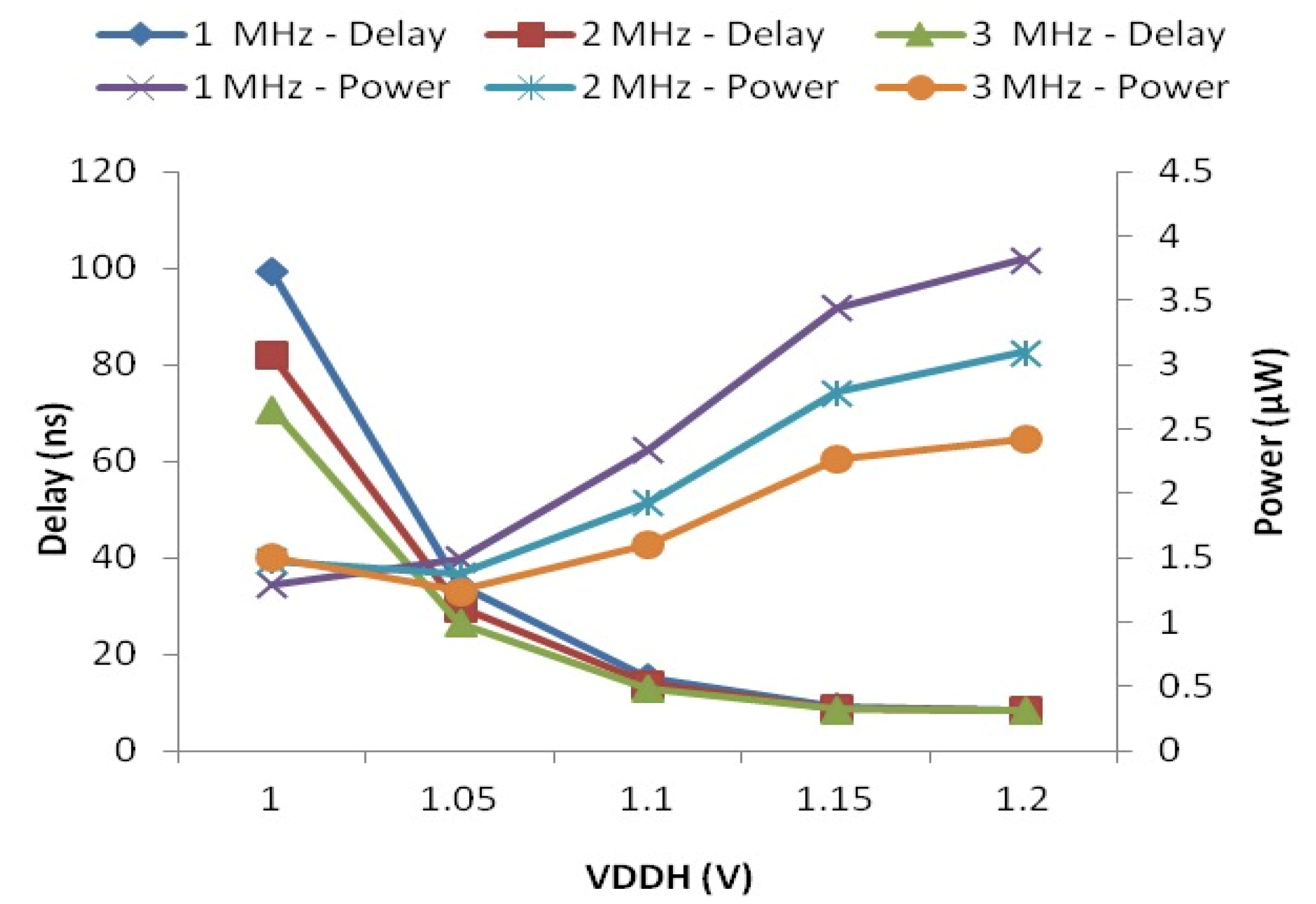
The supply voltage in digital circuits at a high level of VDDH can have a noteworthy impact on the power of a circuit. Power is usually described as a function of VDDH in the realm of digital design. This connection is crucial to optimizing power efficiency. In particular, a formula incorporating VDDH that is increased to a capacity of two, thereby demonstrating its quadratic impact upon power use, can be used to determine the power used by an electronic circuit. This illustrates how vital the supply voltage is when figuring out how energy-efficient digital circuits are. The power consumption could be drastically reduced by lowering the VDDH. But, since lower supply voltages generally cause longer delay times as a result of the reduced strength of signals, that decrease usually comes at the cost of speed. The swing is shown in
Figure 12. Therefore, one of the major issues in modern electronic circuits is to find an acceptable balance between power efficiency and performance. The length of time required for a signal to move from the input of a digital circuit into its output is referred to by the term propagation delay. Transistors can transition states faster, as the threshold value of the transistor decreases in conjunction with the voltage of the supply VDDH. The time to propagate decreases when the threshold voltage drops. There is a trade-off to be made, however; although the lower VDDH reduces the delay of propagation, it also reduces the margin of noise in the circuit and could make it more vulnerable to noise from the surrounding environment and other process changes.
In digital circuits, the threshold voltage of transistors can have a significant impact on the time to propagation. The threshold voltage of transistors is lowered, along with a decrease in the voltage of supply at low level VDDL. In the event of lowering the threshold voltage, switching speeds could be increased. This can decrease the duration of propagation. The reduction of VDDL could, however, lower the noise margin and increase susceptibility to changes in process and noise, as in the case of the high-level supply voltage. The power consumption is in a different relationship than VDDL. The general rule is that decreasing power supply voltages at the low and high levels, VDDH and VDDL, will reduce power consumption. In contrast to the reduction of VDDH, the reduction of VDDL typically has less of an effect on reducing power. This is because VDDH is the dominant factor in the equation of power consumption, while VDDL has a linear or lesser-than-quadratic impact on power. The propagation delays, power consumption, as well as VDDL trade-offs are similar with those of VDDH, but they are somewhat different in the sense of size and importance. Although reducing VDDH can result in higher energy savings than cutting VDDL, reducing VDDL could only decrease the time to propagate. Like VDDH, the parameters should be adjusted by the designers in accordance with the specific requirements of the specific application. The less-powerful VDDL is a good choice for low-power applications where speed is not an essential factor. However, it is possible to select the higher VDDL for high-performance systems to ensure efficiency while also reducing power consumption, according to
Figure 13.
Table 1 describes the delay and energy of the standard and proposed LSs. It depicts the contrast of the proposed FDLS to the best benchmark designs. The FDLS with full swing transistors makes a short circuit current between VDDH to GND through P5-N6, which are controlled by the current-aware device N7, which has been used here to limit the current under a situation that drags the delay to a very low value compared to other LSs. The OUT node has a lesser swing than the noise margins due to V
GSN7 and V
DSN7 being between the gate and the source as well as the drain and source voltages of the N7 transistor. As a consequence, our proposed FDLS achieves overall enhancements in quite a lot of performance metrics.
The minimum VDDL to convert to 1.20 V is 0.10 V, with a best case of 0.20 V. At 0.20 V and 27 °C, an 8.38 ns delay and 26.64 fJ energy consumption is achieved at 1 MHz input. The number of transistors required is 12 of the proposed state-of-the-art FDLSs, with an extremely competitive semiconductor area, and to some extent an increased energy per transition. The energy of [
25] is 18 fJ, which is low at a convertible VDDL of 0.35 V. But, the proposed FDLA is 26.64 fJ, at a convertible VDDL of 0.20 V. Compared with all the benchmark designs, the proposed FDLS has a low energy and delay. The energy per transition reported in [
26] is on par with FDLS, but the delay is double that of the FDLS and other LSs in [
27], and has huge energy consumption compared with all the LSs.
5. Conclusions
By utilizing a cross-coupled LS and current mirror LS, a hybrid structure was designed. The proposed FDLS is robust for good delay scalability and has a broad range of voltage level shifting, from deep sub-threshold voltage to a core supply voltage. It is an combination of CCLS and CMLS, maintaining their unique advantages while working together to resolve current contention and high static current difficulties. Full swing circuit optimization approaches are also used to increase speed and lower the energy use, delay, and energy consumption of the suggested FDLS. The proposed FDLS implemented by using 45 nm CMOS technology in Cadence tools and the simulation results prove that the circuit topology offers low propagation delay and good performance, with a supply voltage from 0.20 V to 1.20 V. At a level shifting voltage of 0.20 V, a 1 MHz input frequency in the proposed FDLS out performs, with a propagation delay of 8.38 ns, average power consumption of 3.81 µW, and an energy per transition of 26.64 fJ at 27 °C.


 ,
, 


