Article

A Method for Improving Radio Frequency Rectification Efficiency in Low-Resistance Loads

College of Electronics and Information Engineering, Sichuan University, Chengdu 610065, China
*
Author to whom correspondence should be addressed.
Electronics 2024, 13(13), 2496; https://doi.org/10.3390/electronics13132496
Submission received: 1 June 2024 / Revised: 20 June 2024 / Accepted: 24 June 2024 / Published: 26 June 2024
(This article belongs to the Section Power Electronics)

Abstract

:
Present radio frequency (RF) rectifiers usually suffer from poor power conversion efficiency (PCE) at low-resistance loads, and the currently proposed DC-DC converter cannot solve this problem well. Aiming at this above problem, we propose a novel DC-DC converter for rectifiers, which consists of a Boost–Buck circuit and a Buck circuit cascaded together to maintain high PCE at both high and low load resistance; the converter can also operate over a wide range of input powers. The proposed converter, along with a 2.45 GHz rectifier, was fabricated to verify its performance. With the converter, the load range of the rectifier when the overall PCE is over 50% was extended from 250 Ω–1250 Ω to 5 Ω–3000 Ω. The highest overall PCE reached up to 61% and the overall PCE at a small load of 5 Ω increased from 1.1% to 54%. The proposed converter can be used in wireless power transmission (WPT).

1. Introduction

RF rectifying circuits are crucial in the microwave field to convert microwave energy into DC energy [1]. They have been widely used in wireless charging, radio frequency identification (RFID) systems, and energy harvesting systems [2,3,4]. However, one of the paramount problems with the present rectifiers [5,6,7,8] is that they usually suffer from poor conversion efficiency at low-resistance loads. Low-resistance loads may cause inefficiencies in the system, resulting in energy waste. For some devices, such as motors, batteries, speakers, and small light bulbs, their resistance is so low that they cannot be directly utilized in RF rectifying circuits.
Many researchers have studied rectifiers with a wide load range and have proposed various topologies. In [9], a maximum power point tracking (MPPT) method was proposed, which achieved high rectification efficiency from 100 Ω to 5000 Ω and an overall RF-dc–dc efficiency of over 60%. In [10], a rectifier based on the reflected power compensation network (RPCN) was designed, which could maintain a relatively high PCE (over 50%) when the load range varied from 8 kΩ to 97 kΩ at an incident power of 7.5 dBm. In [11], a novel rectifier based on a branch-line coupler was presented. The proposed rectifier improved the bandwidth range of the load and achieved an efficiency of over 50% when the load was 50 Ω. In [12], two compact patch rectennas, whose rectification efficiency could exceed 70% when the load was 50 Ω, were presented, and the proposed rectenna does not require matching networks. In [13], a reconfigurable rectifier with two operation modes was presented. The rectifier can operate under a load of 50~1500 Ω, with the maximum output power reaching 12 mW. However, the above technologies still cannot achieve high PCE under extremely low-resistance loads.
Another approach to maintaining high PCE over a wide load range is using DC-DC converters. The commonly used DC-DC converters in energy harvesting systems are Boost–Buck converters [14,15], Buck converters [16], and Boost converters [17]. Usually, the input impedance of these converters will be influenced by load if it is small. At present, many novel converters have also been proposed [18,19,20,21], but they mostly operate under high-power conditions for boosting and bucking. Therefore, there has been little discussion on the applicable range of load values.
The above methods are basically unable to effectively solve the problem of poor rectification efficiency of the RF rectifier under low-resistance loads. To address this problem, this paper proposes a DC-DC convert for RF rectifiers to maintain high PCE under low-resistance loads. The proposed converter consists of a cascaded Boost–Buck circuit and Buck circuit, which provides a stable input impedance under low-resistance loads to enable the rectifier to achieve maximum power transfer. In addition, it can operate over a relatively wide input power range and also have a relatively wide load impedance range. The maximum PCE of the proposed converter is 85%.
The subsequent sections are structured as follows: Section 2 describes the basic structure of the rectifier circuit. Section 3 introduces the basic principle and implementation process of the proposed DC-DC converter. Section 4 describes the experimental results and analysis. Section 5 summarizes the findings and contributions of this work.

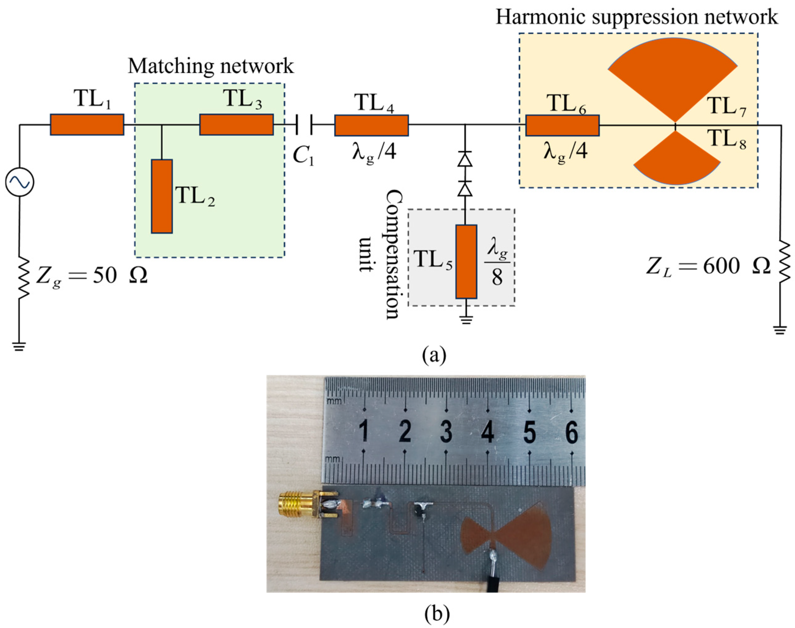
2. The Structure of the Rectifier Circuit

The designed rectifier is shown in Figure 1, which is a typical shunt rectifier and mainly consists of the following three parts: the matching network, the imaginary part compensation unit [22], and the harmonic suppression network. The used Schottky diode is HSMS282C. This circuit works at a frequency of 2.45 GHz. When the input power is 28.5 dBm, it achieves its maximum rectification PCE of 71.7%, which means that the maximum power obtained by the load is 510 mW. This power can be applied to motors and speakers with an operating voltage of 2 V and can also charge low-capacity batteries.

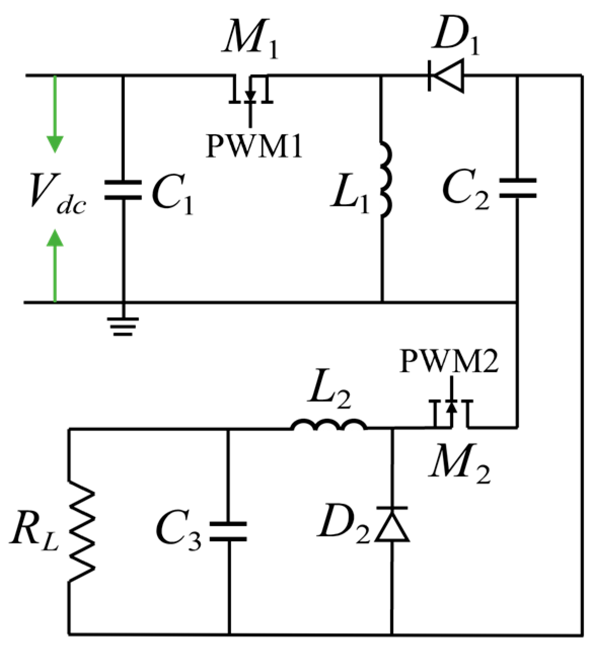
3. The Proposed DC-DC Converter

Microwave can be used in WPT to achieve long-distance energy transfer. At present, the proposed rectifier cannot be directly applied to low-resistance loads. DC-DC converters can be combined with rectifiers to achieve efficient energy conversion under low-resistance loads. The proposed DC-DC converter can charge the battery or drive some low-resistance devices, thus simplifying the design of the driving circuit.
The schematics of the Boost–Buck circuit and Buck circuit are shown in Figure 2a,b. When the load resistance is small, the current through the inductance is continuous, and the circuit is in continuous conduction mode (CCM). When the load resistance is large, the current through the inductance is discontinuous, and the circuit is in discontinuous conduction mode (DCM), as shown in Figure 3a,b.
According to [14], when the load resistance is large and the Boost–Buck circuit is in DCM, its input impedance is independent of the load, meaning a constant input impedance can be realized. Its input impedance is
R i n 1 = 2 L 1 f s 1 D 1 2 ,
where D1 is the duty cycle of the PWM1 signal, fs1 is the frequency of the PWM1 signal, and L1 is the circuit’s inductance. However, when the load resistance RL is small and the Boost–Buck circuit is in CCM, its input impedance is [14]
R i n 1 = 1 D 1 1 2 R L .
According to (2), the input impedance will be affected by the load resistance. Thus, the Boost–Buck circuit is not suitable for rectification at low-resistance loads.
The input impedance of the Buck circuit in DCM is [14]
R i n 2 = 2 L 2 f s 2 D 2 2 U i n 1 U i n 1 U L ,
where Uin1 is the input voltage of the Buck circuit, UL is the load voltage, D2 is the duty cycle of the PWM2 signal, fs2 is the frequency of the PWM2 signal, and L2 is the circuit’s inductance. The input impedance of the Buck circuit in CCM is [14]
R i n 2 = 1 D 2 2 R L .
According to (3) and (4), as long as the duty cycle of the PWM2 signal is appropriately reduced, the Buck circuit can have a large input impedance under low-resistance loads.
The Buck circuit can achieve a high input impedance, and if we cascade the Buck circuit behind the Boost–Buck circuit, the Boost–Buck circuit can work in DCM to obtain a stable input impedance.
By cascading the Boost–Buck circuit and the Buck circuit, we can realize DC impedance matching for low-resistance loads and high-resistance loads. The circuit structure is shown in Figure 4. Using (1) and (2), the critical load value RL0 of the Buck–Boost circuit in DCM can be calculated, which is
R L 0 = 2 L 1 f s 1 1 D 1 2 .
Therefore, as long as Rin2RL0, the Boost–Buck circuit can operate in DCM, which means
R L 2 L 1 f s 1 D 2 2 1 D 1 2 L 2 f s 2 L 1 f s 1 1 D 1 D 2 2 1 .
Assuming that this circuit has no losses and the input energy is equal to the output energy, we can obtain
U i n 2 R i n 2 = U L 2 R L 2 ,
where Uin is the input voltage and UL is the load voltage. The relationship between Uin and UL can be obtained by (7) and (1), which is
U L U i n = R L R i n = D 1 R L 2 L 1 f s 1 .
When RL > Rin, the circuit is used for boosting, and when RL < Rin, the circuit is used for bucking.
According to (1), we choose the appropriate parameters to ensure that the input impedance of the Boost–Buck circuit is about 600 Ω. We select a relatively low frequency and duty cycle to reduce the losses of the MOSFET. For Buck circuits, reducing the duty cycle is beneficial for increasing the input impedance of the Buck circuit, but a too-small duty cycle will affect the performance of the circuit. The suitable parameters of the PWM signals are shown in Table 1. The parameters of the components used in the circuit are shown in Table 2.

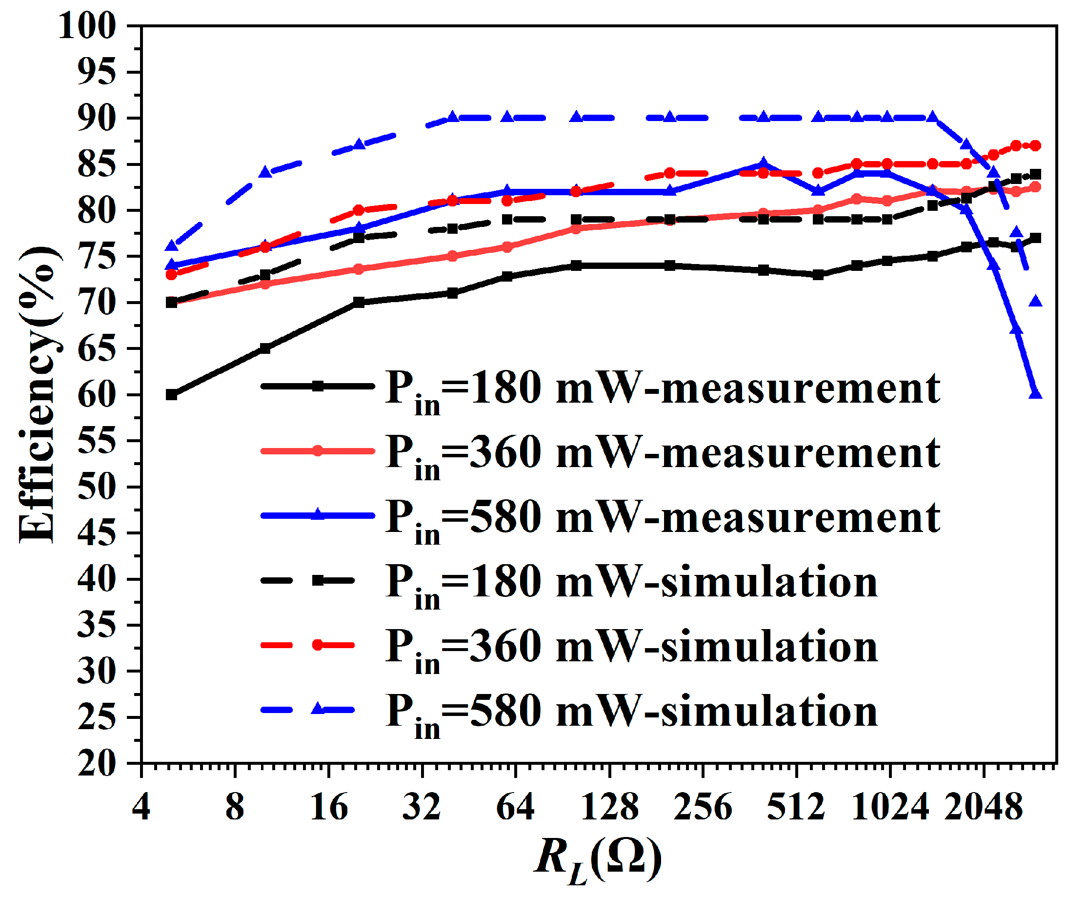
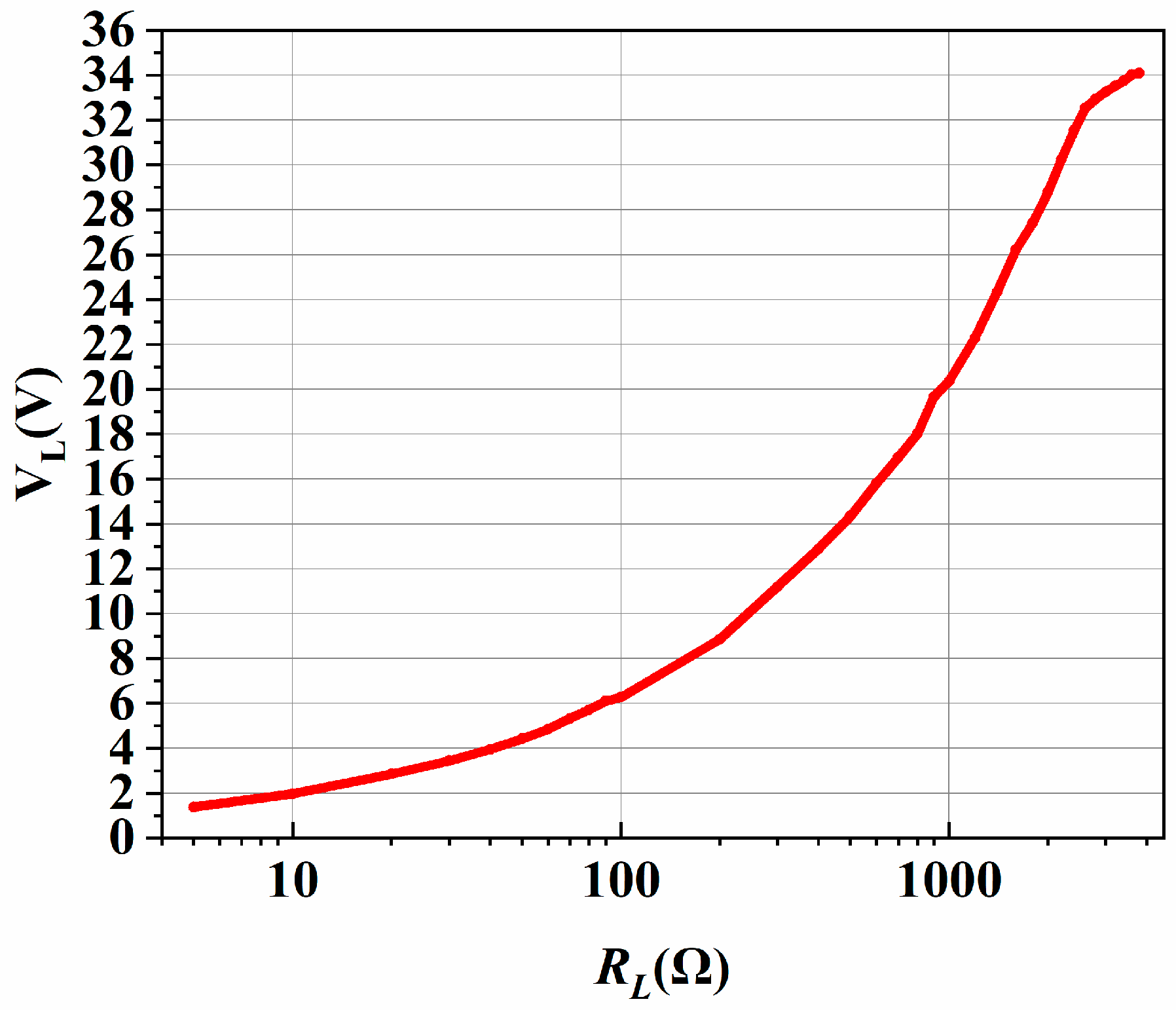
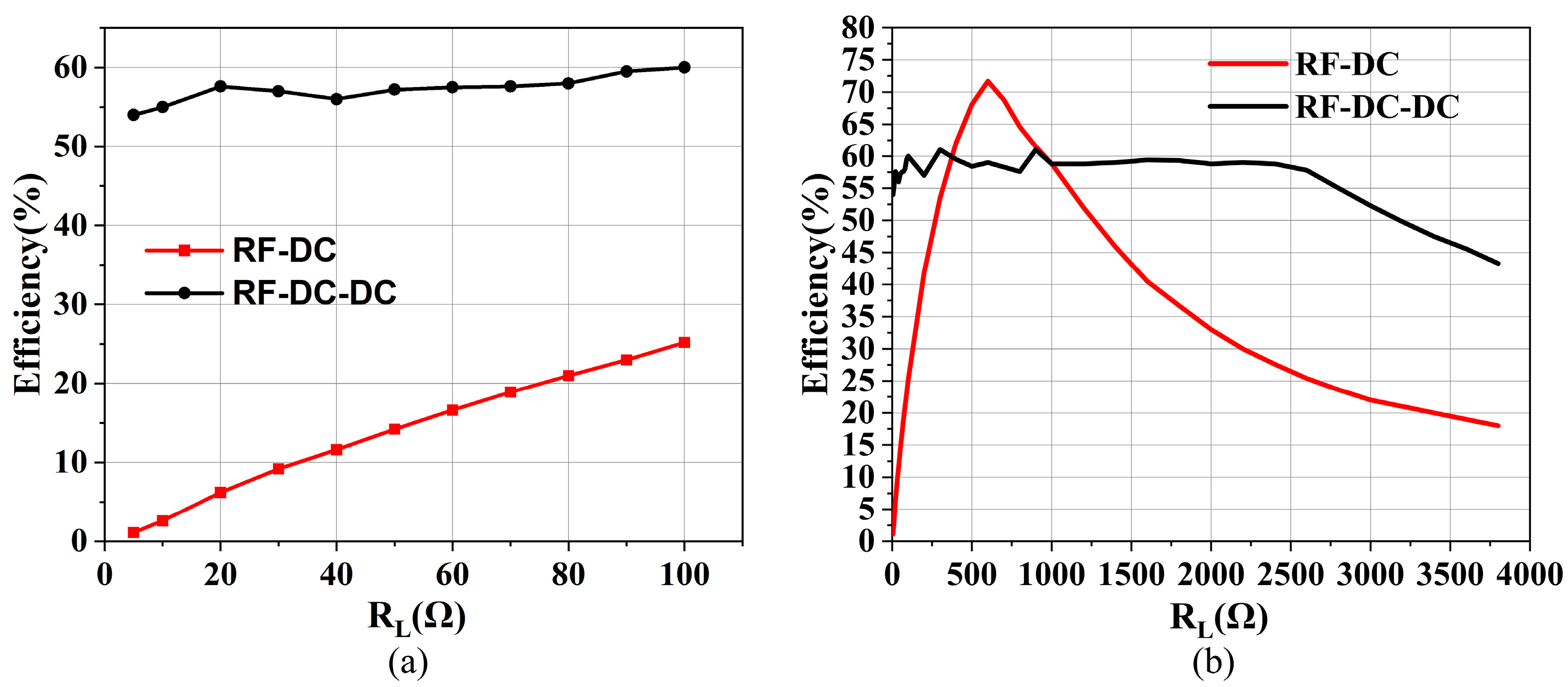
4. Experimental Validation and Discussion

We first tested the efficiency of the designed rectifier with an input power of 28.5 dBm and a frequency of 2.45 GHz. The results are shown in Figure 5. The measured efficiency is consistent with simulation, and the maximum efficiency (71.7%) can be achieved at 600 Ω.
Figure 6a shows the prototype of the proposed DC-DC converter. As shown in Figure 6b, the relationship between the efficiency and input power of this DC-DC converter is simulated and measured under different loads. According to the results, the PCE of the converter increases with the increase in power and eventually stabilizes. When the power is high, its efficiency will decrease because the voltage in the circuit exceeds the normal operating voltage of some devices. Of course, devices with higher withstand voltage values can be chosen, but they will cause greater losses at low power.
Figure 7 shows the relationship between the input impedance of the converter and the load resistance value. Although the input impedance of the converter is affected by input power and load resistance, the input impedance is relatively stable within a certain range of load resistance (5 Ω–3000 Ω).
Figure 8 shows the relationship between the PCE of the converter and the load value at different input power levels. The PCE of the converter is higher than 60% within the power range of 180 mW to 580 mW. As the input power and load resistance value increase, the PCE of the converter will increase and eventually stabilize.
According to Figure 6 and Figure 8, the conversion efficiency of the converter is also affected by input power. Conversion efficiency deteriorates with the decrease in input power, especially for low resistance. The main cause of this problem is that the circuit board produced has certain losses, and the two largest losses are the conduction loss of the Schottky diode and the switching loss of the MOSFET [23]. Because of the ideal devices in the simulation, the conversion efficiency is very high. The main reason for the decrease in efficiency when the load resistance is high is that the voltage on some devices is too high beyond the normal operating voltage range.
Finally, the converter is connected behind the rectifier to measure the load voltage VL and the overall rectification efficiency. Figure 9 shows the relationship between the measured voltage and the load resistance value.
Figure 10a shows the overall PCE under a low-resistance load. When input power is 28.5 dBm, its overall rectification efficiency reaches 54% at 5 Ω. Compared with the efficiency without the DC-DC convert, the overall efficiency increased by 52.9%. Figure 10b shows the overall rectification efficiency exceeds 50% from 5 Ω to 3000 Ω, with a maximum overall efficiency of 61%. According to the results, the converter can greatly improve the overall rectification efficiency when the load resistance is small.
Table 3 shows a comparison between the proposed converter and some prior works. In [9,14], efficient energy transfer was achieved over a wide load range by connecting a Boost–Buck converter behind the rectifier, and the maximum load range with an overall PCE exceeding 50% reached 100~10,000 Ω. However, the converters are not suitable for efficient rectification under low-resistance loads (e.g., 5 Ω), and the maximum power range they can apply to is relatively narrow. In [16], the use of Buck circuits improved the PCE under low-impedance loads, but the load range was narrow. The other converters in Table 3 are not suitable for low-impedance loads. Therefore, our proposed DC-DC converter has significant advantages in improving PCE under low-impedance loads and also has a relatively wide load and power range.
Since the designed rectifier can not only maintain high PCE under low-resistance loads but also has a wide load range, connecting it to the rectifier can adapt to different devices or dynamic loads in the WPT system to ensure maximum energy transmission.

5. Conclusions

In this paper, we have proposed a DC-DC converter that consists of a cascaded Boost–Buck circuit and Buck circuit to improve the load range and PCE of rectifiers, especially at small load resistance. The proposed DC-DC converter has been fabricated and tested. It can provide a stable output impedance for the rectifier and achieve an over 50% PCE when the load resistance is from 5 Ω to 3000 Ω. The PCE at a small resistance of 5 Ω is improved from 1.1%. to 54%. This converter can also operate over a wide input power range with a maximum conversion efficiency of 85%. The DC-DC converter can be used for boosting and bucking and also can be used in power wireless power transmission to achieve maximum power transmission. In the future, we will continue to optimize the performance of the proposed converter to improve its energy conversion efficiency and achieve higher integration.

Author Contributions

Conceptualization, Z.J., H.Z. and Y.Y.; methodology, Z.J.; validation, R.L. and Z.J.; writing—original draft preparation, Z.J. and R.L.; writing—review and editing, Y.Y.; project administration, H.Z. All authors have read and agreed to the published version of the manuscript.

Funding

This research was funded by the National key research and development plan (Grant number: 2023YFB4603500), Hefei major projects (Grant number: 2022-SZD-004).

Data Availability Statement

The original contributions presented in the study are included in the article, further inquiries can be directed to the corresponding author.

Conflicts of Interest

We declare that we do not have any commercial or associative interests that represent a conflict of interest in connection with the work submitted.

References

  1. Hemour, S.; Zhao, Y.; Lorenz, C.H.P.; Houssameddine, D.; Gui, Y.; Hu, C.M.; Wu, K. Towards Low-Power High-Efficiency RF and Microwave Energy Harvesting. IEEE Trans. Microw. Theory Tech. 2014, 62, 965–976. [Google Scholar] [CrossRef]
  2. Wang, N.X.; Wang, H.W.; Mei, J.; Mohammadi, S.; Moon, J.; Lang, J.H.; Kirtley, J.L. Robust 3-D Wireless Power Transfer System Based on Rotating Fields for Multi-User Charging. IEEE Trans. Energy Convers. 2021, 36, 693–702. [Google Scholar] [CrossRef]
  3. Kang, H.-B.; Choi, B.-G.; Sung, M.Y.; Chung, J. Dual Field Communication Scheme for UHF (860–960 MHz) Gen2 RFID Chip. Integr. Ferroelectr. 2011, 125, 1–10. [Google Scholar] [CrossRef]
  4. Xu, P.; Flandre, D.; Bol, D. Analysis and Design of RF Energy-Harvesting Systems with Impedance-Aware Rectifier Sizing. IEEE Trans. Circuits Syst. II Express Briefs 2023, 70, 361–365. [Google Scholar] [CrossRef]
  5. Rotenberg, S.A.; Podilchak, S.K.; Re, P.D.H.; Mateo-Segura, C.; Goussetis, G.; Lee, J. Efficient Rectifier for Wireless Power Transmission Systems. IEEE Trans. Microw. Theory Tech. 2020, 68, 1921–1932. [Google Scholar] [CrossRef]
  6. Muhammad, S.; Tiang, J.J.; Wong, S.K.; Iqbal, A.; Smida, A.; Azizi, M.K. A Compact Dual-Port Multi-Band Rectifier Circuit for RF Energy Harvesting. Comput. Mater. Contin. 2021, 68, 167–184. [Google Scholar] [CrossRef]
  7. Zhao, F.; Inserra, D.; Gao, G.; Huang, Y.; Li, J.; Wen, G. High-Efficiency Microwave Rectifier with Coupled Transmission Line for Low-Power Energy Harvesting and Wireless Power Transmission. IEEE Trans. Microw. Theory Tech. 2021, 69, 916–925. [Google Scholar] [CrossRef]
  8. Muhammad, S.; Tiang, J.J.; Wong, S.K.; Nebhen, J.; Smida, A.; Waly, M.I.; Iqbal, A. Broadband RCN-based RF-rectifier with a large range of power for harvesting ambient wireless energy. AEU Int. J. Electron. Commun. 2022, 152, 154228. [Google Scholar] [CrossRef]
  9. Huang, Y.; Shinohara, N.; Mitani, T. A Constant Efficiency of Rectifying Circuit in an Extremely Wide Load Range. IEEE Trans. Microw. Theory Tech. 2014, 62, 986–993. [Google Scholar] [CrossRef]
  10. Song, G.; Liu, X.; Liu, C. Wide-Range Rectifier for Wireless Power Transfer Based on Power Compensation. IEEE Microw. Wirel. Compon. Lett. 2021, 31, 509–512. [Google Scholar] [CrossRef]
  11. Zhang, X.Y.; Du, Z.X.; Xue, Q. High-Efficiency Broadband Rectifier with Wide Ranges of Input Power and Output Load Based on Branch-Line Coupler. IEEE Trans. Circuits Syst. I Regul. Pap. 2017, 64, 731–739. [Google Scholar] [CrossRef]
  12. Liu, C.; Lin, H.; He, Z.; Chen, Z. Compact Patch Rectennas without Impedance Matching Network for Wireless Power Transmission. IEEE Trans. Microw. Theory Tech. 2022, 70, 2882–2890. [Google Scholar] [CrossRef]
  13. Li, Y.; Yan, Y.; Yang, H.; Hu, J.; He, Z. A Reconfigurable Rectifier-Based Power Improving Method of Free-Standing Two-Coil Magnetic Field Energy Harvesters Over a Wide Load Range. IEEE Trans. Power Electron. 2023, 38, 5638–5643. [Google Scholar] [CrossRef]
  14. Huang, Y.; Shinohara, N.; Mitani, T. Impedance Matching in Wireless Power Transfer. IEEE Trans. Microw. Theory Tech. 2017, 65, 582–590. [Google Scholar] [CrossRef]
  15. Fu, M.; Zhang, T.; Zhu, X.; Ma, C. A 13.56 MHz wireless power transfer system without impedance matching networks. In Proceedings of the 2013 IEEE Wireless Power Transfer (WPT), Perugia, Italy, 15–16 May 2013; pp. 222–225. [Google Scholar]
  16. Moriwaki, Y.; Imura, T.; Hori, Y. Basic study on reduction of reflected power using DC/DC converters in wireless power transfer system via magnetic resonant coupling. In Proceedings of the 2011 IEEE 33rd International Telecommunications Energy Conference (INTELEC), Amsterdam, the Netherlands, 9–13 October 2011; pp. 1–5. [Google Scholar]
  17. Dolgov, A.; Zane, R.; Popovic, Z. Power Management System for Online Low Power RF Energy Harvesting Optimization. IEEE Trans. Circuits Syst. I Regul. Pap. 2010, 57, 1802–1811. [Google Scholar] [CrossRef]
  18. Ajami, A.; Ardi, H.; Farakhor, A. A Novel High Step-up DC/DC Converter Based on Integrating Coupled Inductor and Switched-Capacitor Techniques for Renewable Energy Applications. IEEE Trans. Power Electron. 2015, 30, 4255–4263. [Google Scholar] [CrossRef]
  19. Leal, W.C.; Godinho, M.O.; Bastos, R.F.; Aguiar, C.R.d.; Fuzato, G.H.F.; Machado, R.Q. Cascaded Interleaved DC–DC Converter for a Bidirectional Electric Vehicle Charging Station. IEEE Trans. Ind. Electron. 2024, 71, 3708–3717. [Google Scholar] [CrossRef]
  20. Bui, V.C.; Nguyen, M.K.; Duong, T.D.; Vo, D.V.; Lim, Y.C.; Choi, J.H. A Novel Isolated DC–DC Converter for High Step-Down Applications. IEEE Access 2023, 11, 81545–81562. [Google Scholar] [CrossRef]
  21. Yuan, Y.; Peng, N.; Liu, W.; Yi, C. A Linear-Resonant Hybrid Bridge DC–DC Converter. IEEE Trans. Ind. Electron. 2023, 70, 1478–1488. [Google Scholar] [CrossRef]
  22. He, Z.; Lan, J.; Liu, C. Compact Rectifiers with Ultra-wide Input Power Range Based on Nonlinear Impedance Characteristics of Schottky Diodes. IEEE Trans. Power Electron. 2021, 36, 7407–7411. [Google Scholar] [CrossRef]
  23. Ho, T.S.; Ramiah, H.; Churchill, K.K.P.; Chen, Y.; Mak, P.I.; Martins, R.P. Extended Power Dynamic Range and Enhanced Power Conversion Efficiency of a Switched-Capacitor DC–DC Converter: A Tutorial. IEEE Trans. Circuits Syst. II Express Briefs 2024, 71, 1606–1612. [Google Scholar] [CrossRef]
Figure 1. The structure of the rectifier circuit. (a) Schematic diagram. (b) Circuit layout.
Electronics 13 02496 g001
Figure 2. (a) Boost–Buck circuit. (b) Buck circuit.
Electronics 13 02496 g002
Figure 3. (a) CCM. (b) DCM.
Electronics 13 02496 g003
Figure 4. The proposed DC-DC converter circuit.
Electronics 13 02496 g004
Figure 5. Simulation and measurement values of rectification circuit efficiency.
Electronics 13 02496 g005
Figure 6. (a) The fabricated converter. (b) The experimental and simulated relationship between efficiency and input power.
Electronics 13 02496 g006
Figure 7. Experimental and simulated input impedance of this converter.
Electronics 13 02496 g007
Figure 8. Experimental and simulated conversion efficiency of this converter.
Electronics 13 02496 g008
Figure 9. Measured load voltage.
Electronics 13 02496 g009
Figure 10. Measured results. (a) Low-resistance loads. (b) Wide load range.
Electronics 13 02496 g010
Table 1. The parameters of the PWM signal.
PWM SignalFrequencyDuty Cycle
PWM153 kHz24%
PWM220 kHz20%
Table 2. The components in the converter.
ComponentPart No.Description
MOSFET M1 and M2FDS4559VDSS = 60 V;
RDS (on) = 75 mΩ (VGS = 4.5 V)
Inductance L1 and L290125-330UHL = 330 µH; Rdc = 0.05 Ω;
Idc = 8 A
Schottky diodes D1 and D2SS34VRRM = 40 V; VFM = 0.55 V
Table 3. The comparison of DC-DC converters.
Ref.Freq.
(MHz)
DC-DC ConverterLoad Range for Overall PCE > 50%Maximum Conversion Efficiency of the ConverterApplicable Power RangeYear
[17]1960Boost converter in CRM at low power level, in DCM at higher power levelNo discussion87%50 µW~1000 µW2010
[16]13.16Buck converter in CCM4.7 Ω~50 ΩNo discussionNo discussion2011
[9]2450Boost-Buck converter in DCM100 Ω~5000 Ω86%21 mW~102 mW2014
[18]-Boost converter-96.9%20~300 W2015
[11]2450No DC-DC converter50 Ω~450 Ω——2 mW~100 mW2016
[14]2450Boost-Buck converter in DCM100 Ω~10,000 Ω86%No discussion2019
[10]915No DC-DC converter8 kΩ~97 kΩ——0.6 mW~32 mW2021
[12]2450No DC-DC converter50 Ω~200 Ω——20 mW~200 mW2022
[13]5 × 10⁻⁵No DC-DC converter50 Ω~1500 Ω——No discussion2023
This work2450Boost-buck converter in DCM +Buck converter in CCM at low-resistance loads, in DCM at high resistance loads5 Ω~3000 Ω85%180 mW~580 mW2024
Disclaimer/Publisher’s Note: The statements, opinions and data contained in all publications are solely those of the individual author(s) and contributor(s) and not of MDPI and/or the editor(s). MDPI and/or the editor(s) disclaim responsibility for any injury to people or property resulting from any ideas, methods, instructions or products referred to in the content.

