Abstract
In this study, a broadband linearizer design method based on an extended design space is proposed to optimize the design complexity and linearization performance of conventional linearizers for broadband operation. The gain characteristics of the power amplifier (PA) and linearizer are fitted to simplify the analyses and to quickly derive the ideal objective function of the linearizer design. Then, the 1 dB compression point of a nonlinear system is redefined and used to further extend the design space of the linearizer. To verify the proposed design method, a millimeter-wave linearizer prototype based on the extended design space was designed and fabricated. The linearizer was tested with continuous-wave and 100 MHz two-tone signals from 40 GHz to 43 GHz. The measurement results of the linearized PA showed that the output 1 dB power point () was improved by more than 1.7 dB, the phase error was reduced by more than 15, and the third-order intermodulation distortion (IMD3) was suppressed by 8.6 dB–13.1 dB over the working frequencies. The proposed linearizer achieved good linearization performance, low power consumption, and simple design implementation, and it was not necessary to tune the bias during broadband operation, making it applicable in complex communication scenarios.
1. Introduction
Millimeter-wave (MMW) communications can provide richer available spectra and higher data capacity than the conventional sub-6 GHz band; however, the wider RF working bandwidth and signal bandwidth of the MMW band exacerbate conflicts between the energy efficiency and signal quality of communication systems [1,2,3,4]. Linearization techniques can effectively alleviate these conflicts [5,6,7]. Digital predistortion (DPD) techniques are widely used in sub-6 GHz communication systems to maintain good efficiency and linearity; however, the cost and power consumption of DPD increases dramatically with the increase in the RF working bandwidth and signal bandwidth [8,9,10]. Considering that the MMW band has lower limitations on inter-channel interference than the sub-6 GHz band, analog linearization techniques with simple implementations and low power costs are more suitable for MMW communication systems [11,12,13].
Diode-based analog predistortion linearizers are currently among the most widely used analog linearization techniques. A simple open-loop operation allows for extremely low power consumption but limits the linearization performance, especially in broadband operation [12,13,14,15,16,17,18,19,20]. Several new design methods have been proposed to enhance the performance of analog linearizers. The spice model and the measured impedance of the diode were used to predict the performance of a linearizer in [14,15,16]. Vector modulators and multipliers can be utilized to tune the predistortion signals generated by a linearizer [17,18]. The amplitude and phase compensation of a linearizer were decoupled to improve the tuning accuracy and linearization performance in [19,20]. However, bias tuning remains an unavoidable means of enhancing the linearization performance of broadband linearizers at multiple frequencies, leading to increased complexity in both design and use.
Recently, a linearizer design platform based on the minimum amplitude and phase error was proposed in [21]. It was validated for linearizer design in the sub-6 GHz band and demonstrated superior performance; however, the preset objective function for linearizer design on the platform was based on a single frequency, and with the increase in the RF bandwidth in MMW communication, the difficulty of synthesizing linearizer design using multi-frequency objective functions increased dramatically. Considering the reduced requirement for linearity in the MMW band, simplified design and fast synthesis for broadband operation in exchange for a small reduction in linearization performance are conducive to the widespread use of linearizers.
In this study, the gain curves of a PA and linearizer are fitted to simplify the analysis and quickly derive the ideal objective function of the linearizer. Because the design goals of a broadband linearizer at different frequencies are difficult to satisfy simultaneously, the 1 dB compression point of a nonlinear system was redefined and used to extend the design space of the linearizer. Based on the extended design space, a broadband linearizer was then designed to verify the proposed design method. The linearizer was tested with continuous-wave and two-tone signals from 40 GHz to 43 GHz, and good linearization performance was achieved with a simple design and implementation.
This study is organized as follows. In Section 2, the extended design space for linearizers is proposed and analyzed. In Section 3, a linearizer prototype based on the extended design space is presented. The linearization platform setup and measurement results are described in Section 4. Finally, the conclusions of this study are presented in Section 5.
2. Theory and Analysis
2.1. Three-Segment Fitting of Gain Curves for a PA and Linearizer
The schematic of a cascaded linearizer–PA system for linearization is shown in Figure 1a. The input power of the linearizer is defined as , the output power of the linearizer and the input power of the PA are defined as , and the output power of the PA is defined as . By using the linearizer, the input 1 dB compression power () and output 1 dB compression power () of the PA can be extended.
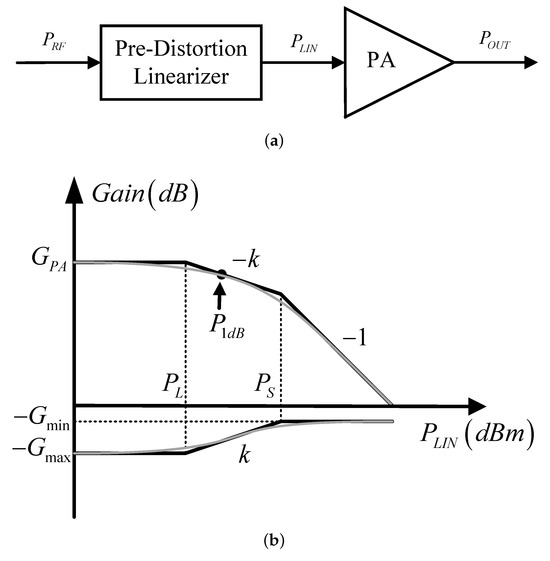
Figure 1.
(a) Schematic of the cascaded linearizer–PA system for linearization. (b) Fitting of the gain curves of the PA and predistortion linearizer.
To design a predistortion linearizer with effective compensation, the gain curves of the PA and linearizer should be inverse. To analyze the curves naturally, real gain curves, shown by the gray lines in Figure 1b, were fitted to three line segments, shown by the black lines [22].
The gain curve of the PA versus its input power () exhibits gain compression features, as shown at the top of Figure 1b. The first segment characterizes the gain features with a small input power; the PA works in the linear region, and the gain was fixed at . The second segment is the tangent line of the real gain curve at , the slope of which is ; this was used to fit the gain compression region. The third segment was used to model the gain curve of the PA in the saturation region. In this region, the output power is constant and invariant with the input power changes, and the gain has a negative correlation with the input power. The input power that the gain of the PA starts to compress is defined as , and the power at which the output power stops increasing is defined as .
The gain of the linearizer versus its output power () with the gain compensation feature is depicted at the bottom of Figure 1b. It was easier to calculate the gain compensation curve versus its output power than versus its input power, as the gain of the linearizer could be added to the gain of the PA using the same reference.
For an actual PA, the , , and are known and constant, allowing the gain compensation curve to be determined. In order to minimize the distortion due to gain compression, the slope of the gain compression region needs to be eliminated. Through simple mathematical derivation, it is easy to find that the gain compensation curve needs to be symmetrical with respect to the gain compression curve. As shown at the bottom of Figure 1b, the gain of the linearizer increases with slope k when the gain of the PA decreases with slope . Note that if the PA works in the linear region or the saturation region, the gain of the linearizer does not improve the linearity; this, the gain of the linearizer was fixed to in the linear region and in the saturation region in order to simplify the design.
Using the gain compensation curve of the linearizer versus its output power in Figure 1b, it can be easily found that the gain of the linearizer can be written as
Moreover, the gain function of the linearizer is provided by
According to (1) and (2), the ideal gain of the linearizer versus its input power can be simply derived as follows:
Based on the gain characteristics of the PA and Equation (3), the objective function for the design of the linearizer can be calculated, and the linearized PA achieves good linearity when the gain of the linearizer complies with Equation (3). However, it is difficult for broadband linearizers and PAs to simultaneously satisfy the gain functions in (3) at different frequencies. The conventional linearizer control method for improving broadband performance by adjusting the bias voltage is not applicable to complex communication scenarios. The objective function of the linearizer requires an extension of the solution space in order to fit the design theory of broadband linearizers without bias tuning. The 1 dB compression point of the PA is usually used to evaluate its linear output capabilities, and can be used to extend the design space of linearizers to some degree.
2.2. Extension of the Definition of the 1 dB Compression Point
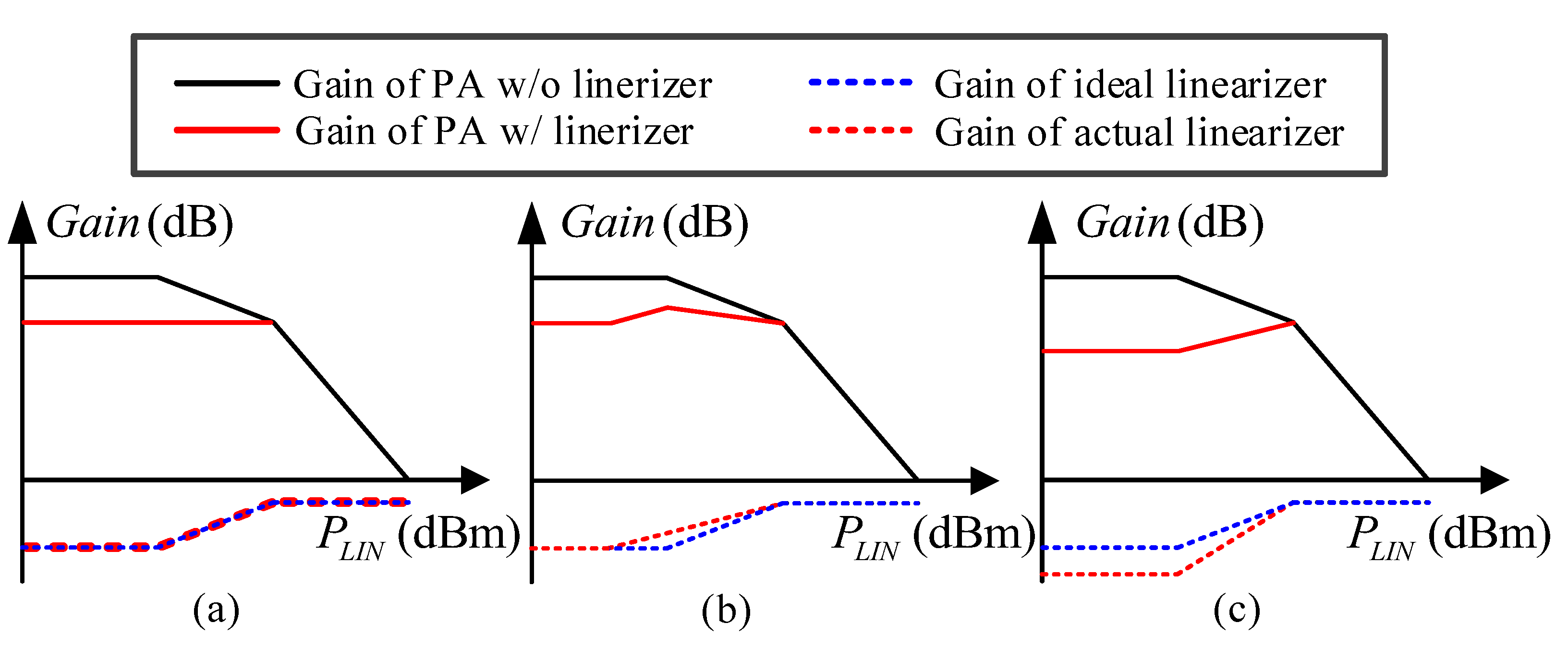
The 1 dB compression point of the PA is defined as the actual gain compressed by 1 dB compared with the linear gain; the output power of the PA at that point is usually considered the maximum output with good linearity [23]. The gain characteristics of a cascaded linearizer–PA system are more complex than those of a PA. For an ideal linearizer, as shown in Figure 1b, the gain compression characteristics of the PA can be fully compensated without introducing additional gain fluctuations. The actual linearizer–PA system exhibits gain expansion characteristics, as the gain expansion turn-on point of the linearizer is earlier than the gain compression turn-on point of the PA or the linearizer overcompensates for the gain compression of the PA, as shown in Figure 2.
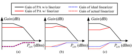
Figure 2.
Gain curves of different linearizer–PA systems: (a) ideal compensation, (b) gain expansion due to earlier turn-on, and (c) gain overcompensation.
Because a PA may exhibit gain expansion characteristics after using a linearizer, and because the nonlinearity produced by gain expansion or compression of 1 dB is comparable for nonlinear systems, the conventional definition of the 1 dB compression point of the PA needs to be extended to match that when the gain of the system first fluctuates by 1 dB from the small-signal gain. This can be achieved through either gain expansion or gain compression. The input and output power at this point is then defined as the 1 dB power point for the system.
Similarly, the conventional definition of the PA’s linear output power range when using the 1 dB compression point can be extended. In this case, the design goal of the linearizer is redefined as ensuring that the gain fluctuation of the linearized PA system in comparison with the small-signal gain is less than 1 dB over the dynamic range of the input, which provides more space for the design of linearizers.
2.3. Design Space Extension for Broadband Linearizers
This section provides an analysis of the gain characteristics of the design space of the linearizer based on the redefined linearizer design goal from the previous section. The phase characteristics can usually be compensated for by optimizing the design of the PA; thus, the analysis in this section can be used when phase compensation is required.
For the fitting curve of the gain in Figure 1b, the minimum gain of the linearizer was assumed to be 0 dB in order to simplify the analysis, which was achieved by tuning the gain of the small-signal amplifier to compensate for the insertion loss of the linearizer. The expanded gain space of the linearized PA system is shown by the shaded area in Figure 3. The x-axis represents the input power of the PA, i.e., the output power of the linearizer. The power range of the shaded area is from the PA’s gain compression turn-on point to the saturation input , and the gain range is the gain fluctuation of 1 dB in comparison with the linear gain of the PA. A linearized PA can be considered to achieve good linearity when the gain curves of the cascaded linearizer–PA system are within the shaded area, as shown in Figure 3.
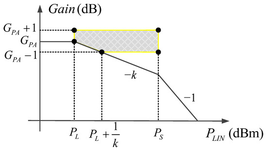
Figure 3.
Expanded gain space of the linearized PA system (shaded area).
It can be seen in Figure 3 that the output power of the gain expansion turn-on point of the ideal linearizer should be equal to ; however, power limitations lead to increased complexity of linearizer design. In this section, three cases are analyzed where the gain expansion turn-on point of the linearizer is equal to, greater than, and less than .
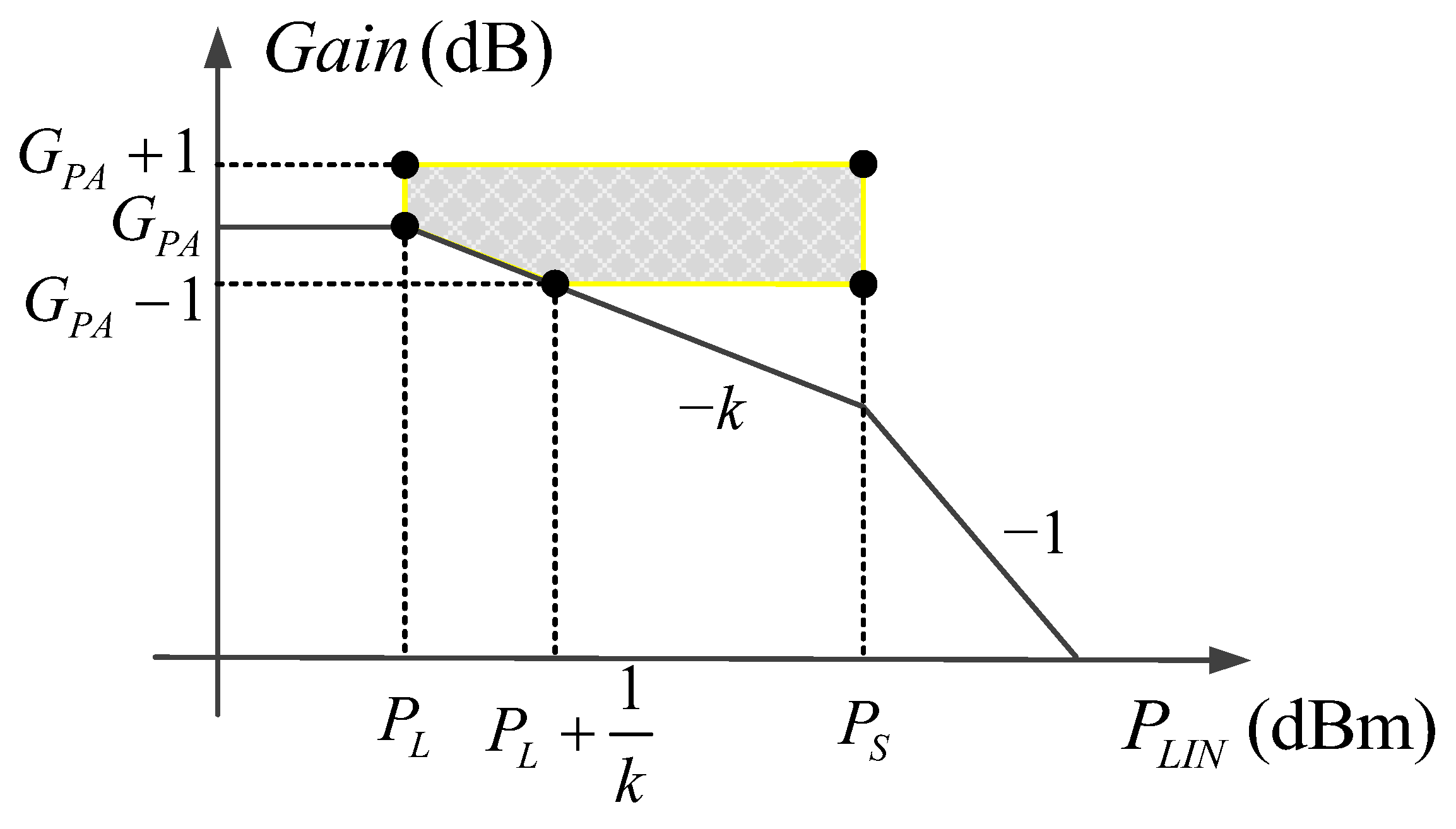
2.3.1. The Gain Expansion Turn-On Point Is Equal to
Figure 4 shows a partial view of the shaded area from Figure 3; the endpoints of the area are labeled using the power and gain, and the area is the gain space of a cascaded linearizer–PA system with good linearity. Because the gain expansion turn-on point of the linearizer is equal to , it can be seen that the cascaded gain curve crosses the point of .
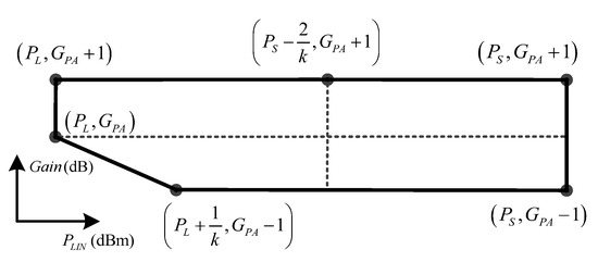
Figure 4.
Gain space of the cascaded system with good linearity.
First, the maximum expansion slope available for the design of the linearizer is analyzed. It can be seen in Figure 4 that the cascaded gain cannot be greater than when the power is less than . On the one hand, assuming that the cascaded gain is equal to at a power of less than , if the gain of the linearizer continues to expand, then the cascaded gain will be more than with the power increase. Thus, the linearization design goal of ensuring that gain fluctuations are less than 1 db is not achieved. If the gain of the linearizer is kept constant, then the gain compression of the PA from the power of to the saturated power point will be more than 2 dB, making the cascaded gain less than ; again, the goal of the linearization design is not achieved. Usually, the saturation power of a PA is defined as the output power with gain compression of 3 dB or more. From the gain curve of the PA shown in Figure 1b, it can be found that
where . Equation (4) can be rewritten as
Notably, all of the analyses in this section based on Figure 4 are restricted to the power–gain relationship given in (5).
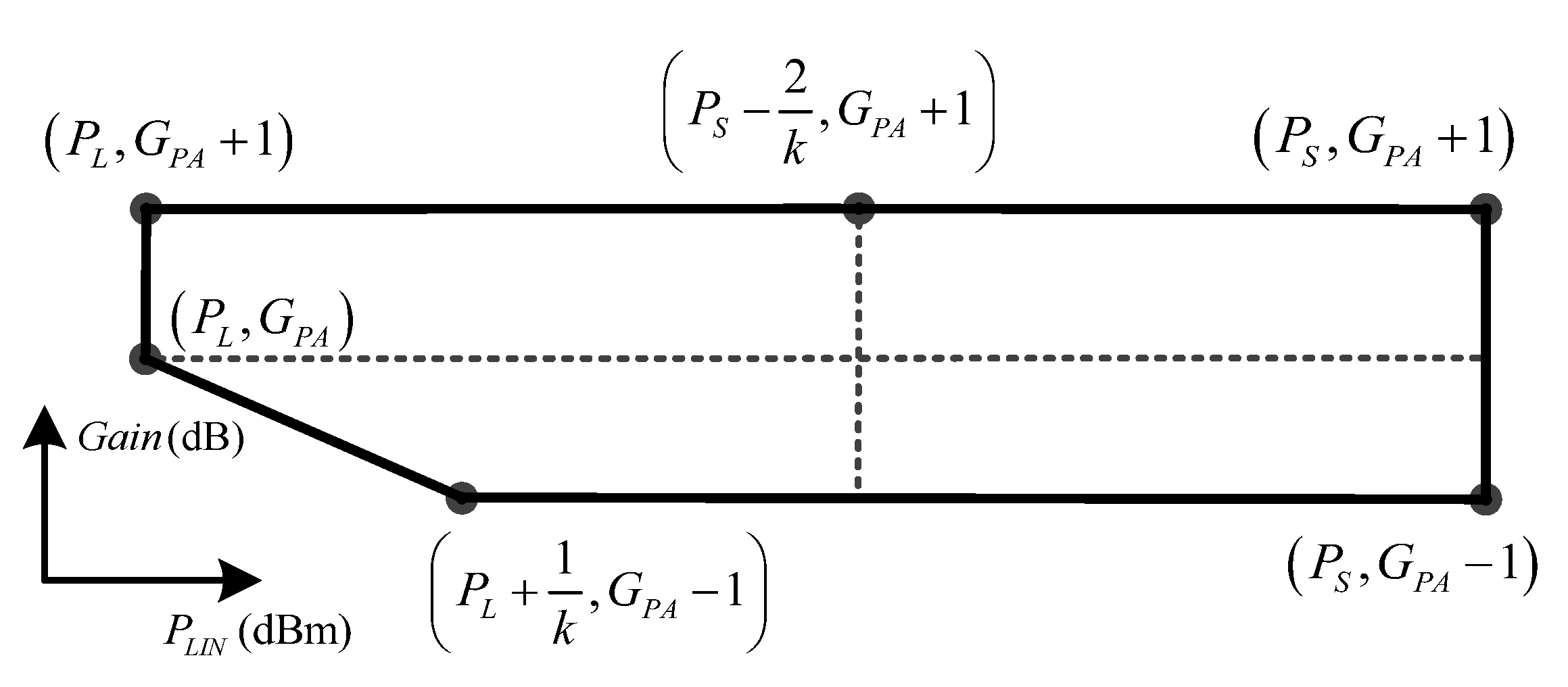
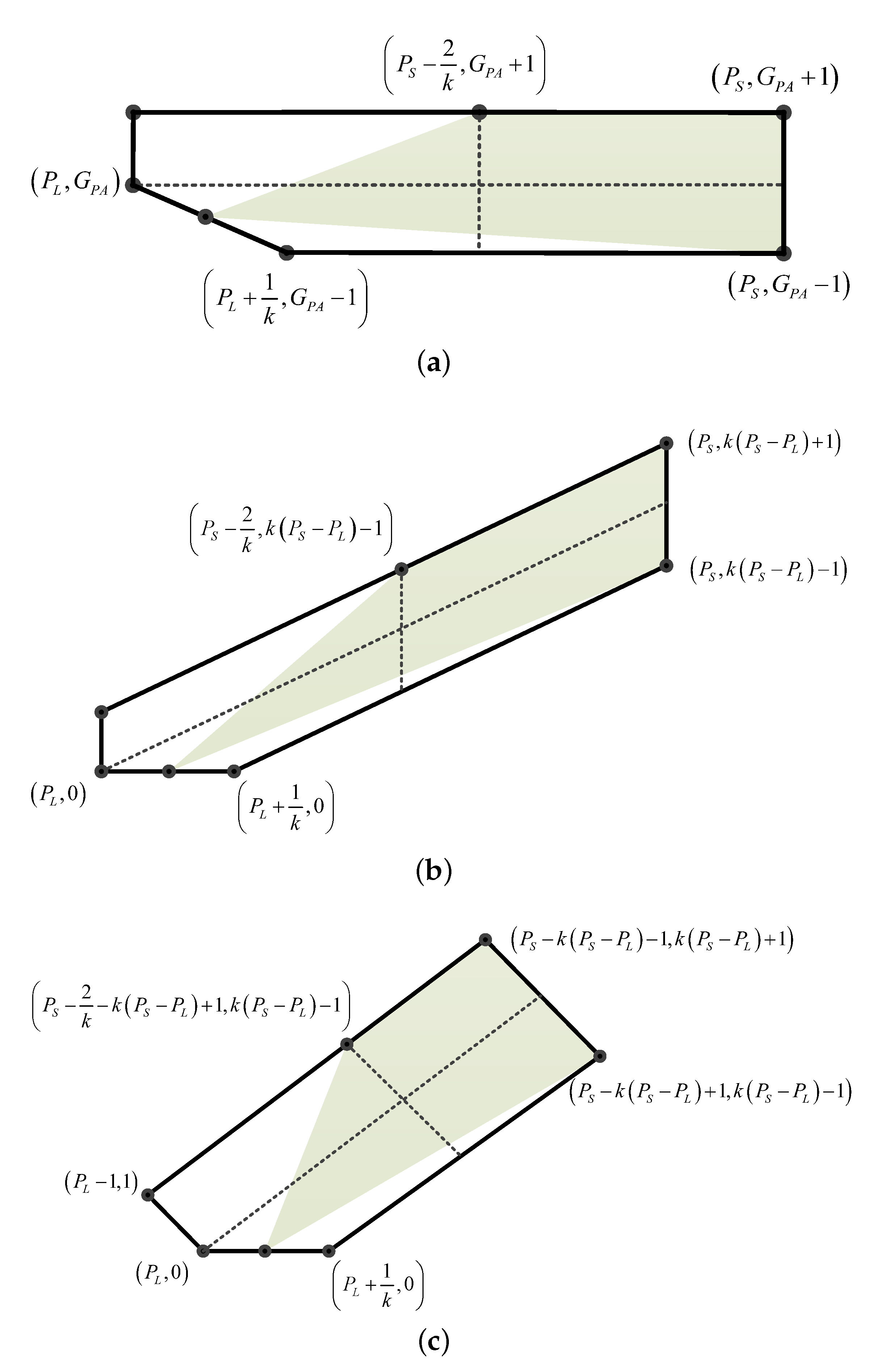
Next, the minimum expansion slope available for the design of the linearizer is analyzed. Similar to the analysis of the maximum slope, it is obvious that the cascaded gain cannot be less than when the power is less than , otherwise the linearization design goal is not achieved. Based on the above analysis, the cascaded gain design space in which the gain characteristics of the linearizer and PA begin to change simultaneously (i.e., the gain expansion turn-on point is equal to ) and achieve the linearization design goal is shown by the shaded area of Figure 5a.
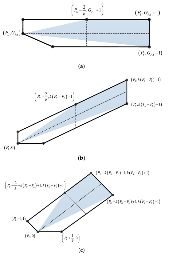
Figure 5.
Design gain space of (a) a cascaded system with the same turn-on point, (b) a linearizer versus its output, and (c) a linearizer versus its input.
It should be noted that the gains mentioned in the analysis in this section correspond to a power-independent variable . The cascaded gain can be written as
According to the gain of the PA, as shown in Figure 1b and Equation (6), the design gain space of the linearizer versus its output power is presented in the shaded area of Figure 5b. Then, the design gain space of the linearizer versus its input power can be obtained from (2), as shown in the shaded area of Figure 5c. The area is the objective gain space of the linearizer design. The linearizer–PA system is able to achieve the preset linearization goal if its cascaded gain curves are located in the shaded area shown in Figure 5c. Similar analyses can be used when the gain expansion turn-on point of the linearizer is greater or less than .
2.3.2. The Gain Expansion Turn-On Point Is Less than
For the case in which the gain expansion turn-on point of the linearizer is less than , the gain characteristics of the linearizer have two operating states (expanding and constant); thus, the gain of the linearizer at the output power of should achieve the following condition:
which can make the cascaded gain fluctuation less than 1 dB. The cascaded gain design space that achieves the linearization design goal is shown in the shaded area of Figure 6a. The cascaded gain at the power of can be any value from to . Similar to the previous analysis, the gain design space of the linearizer versus its output power can be seen in Figure 6b, and the space versus input power can be seen in Figure 6c.
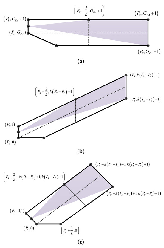
Figure 6.
Gain design space of (a) a cascaded system with an earlier linearizer turn-on, (b) a linearizer versus its output, and (c) a linearizer versus its input.
2.3.3. The Gain Expansion Turn-On Point Is Greater than
For the case in which the gain expansion turn-on point of the linearizer is greater than , the turn-on point of the linearizer obviously cannot be greater than , otherwise the gain compression would exceed 1 dB and the linearization design goal would not be achieved. The cascaded gain design space with later linearizer turn-on is shown in the shaded area of Figure 7a, while the gain design space of the linearizer versus its output and input power can be seen in Figure 7b and Figure 7c, respectively.
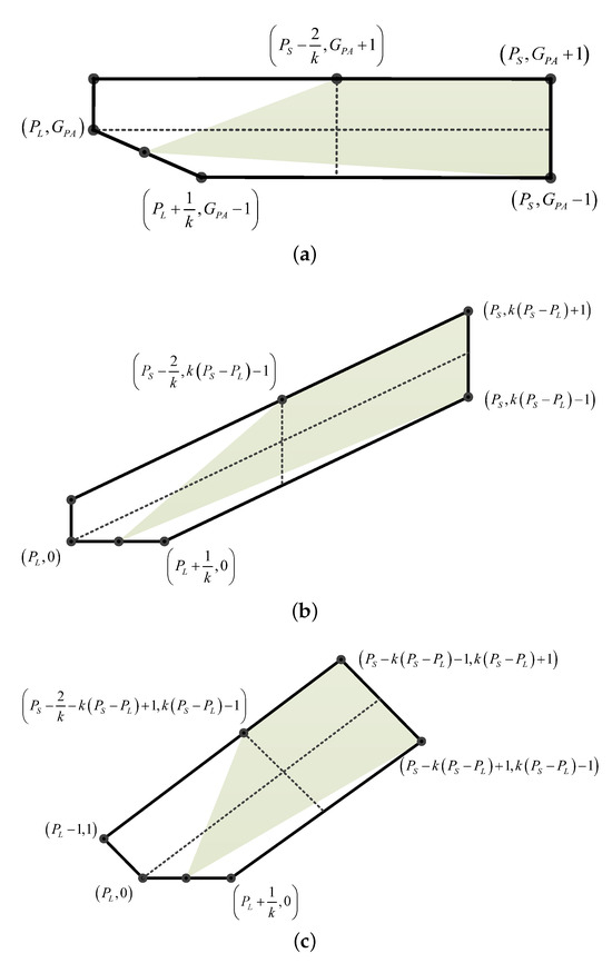
Figure 7.
Gain design space of (a) a cascaded system with a later linearizer turn-on, (b) a linearizer versus its output, and (c) a linearizer versus its input.
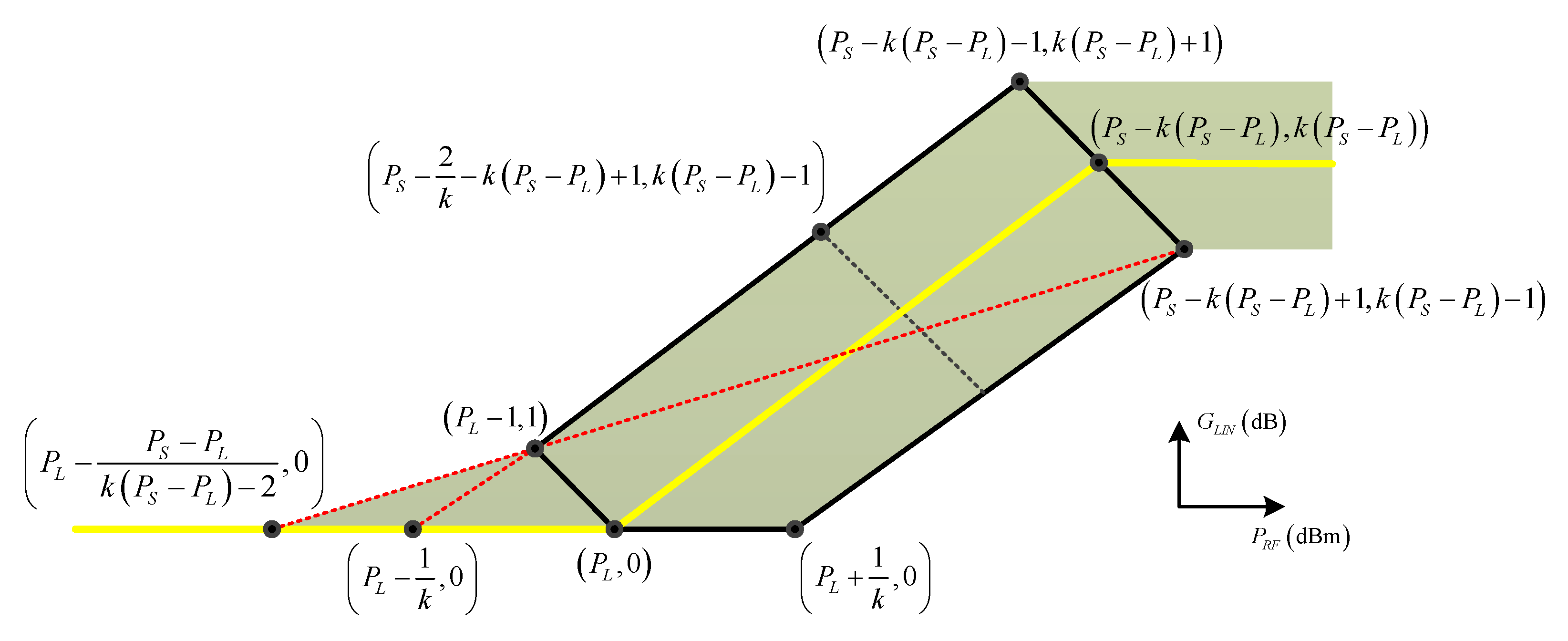
According to Figure 5c, Figure 6c, and Figure 7c, the expanded gain design space of the linearizer can be obtained as shown in Figure 8. The yellow line in Figure 8 is the ideal gain curve of the linearization design, and the green area shows the expanded design space based on the proposed definition of the 1 dB power point. It should be noted that when the output power of the linearizer is greater than , as indicated by the green area on the right side of the black box line in Figure 8, the PA operates in the saturation region and the linearizer does not have sufficient compensation capabilities to improve the linearity of the PA; thus, the characteristics of linearizer in this region do not need to be considered in the design process. When the gain characteristics of the designed linearizer fall within the green region, those of the cascaded linearizer–PA system achieve the preset linearization goal, that is, the linearized PA has a gain fluctuation of less than 1 dB compared with its small-signal gain before it reaches saturated output power.
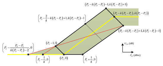
Figure 8.
Expanded gain design space of the linearizer.
3. Linearizer Design Based on the Extended Design Space
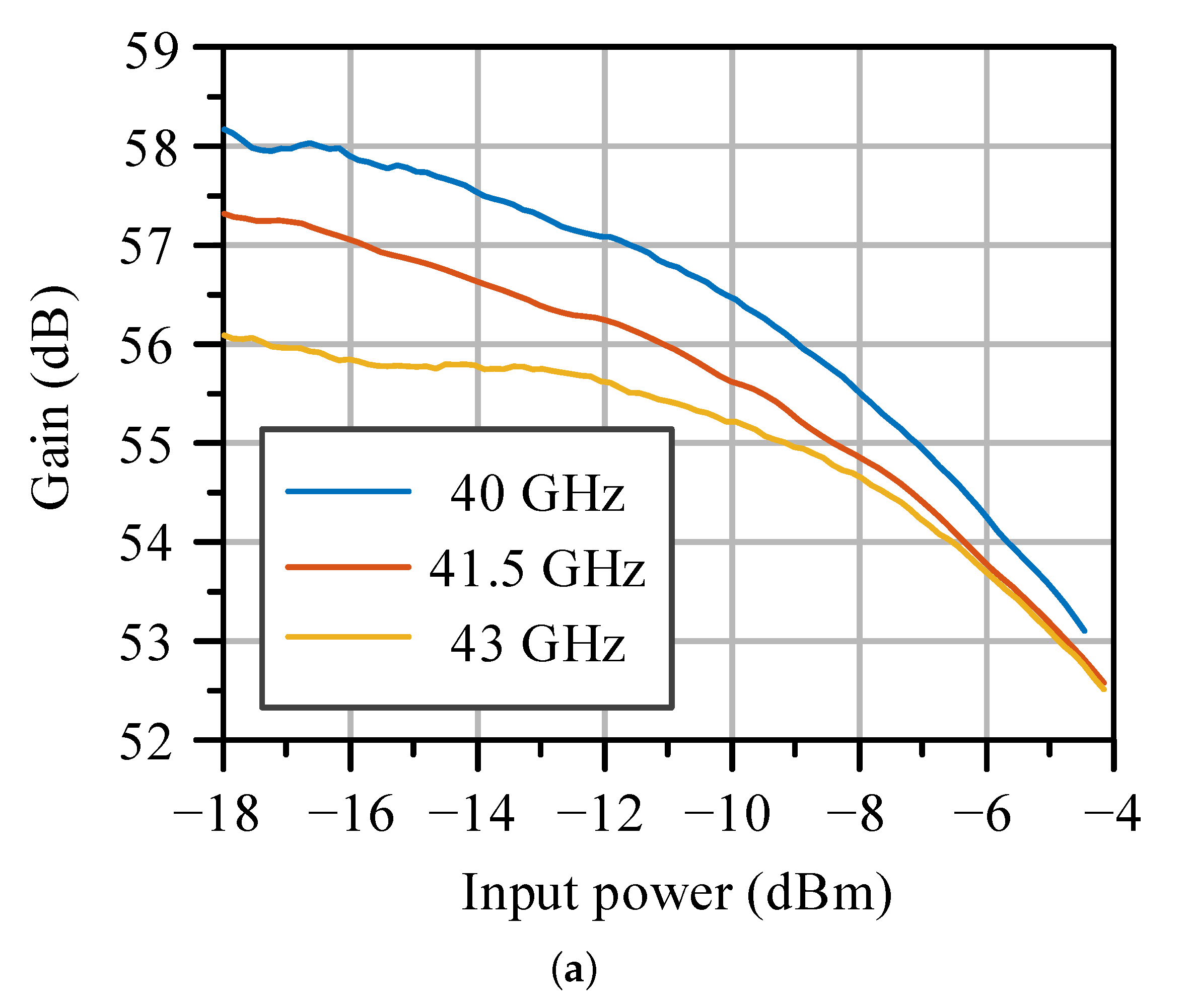
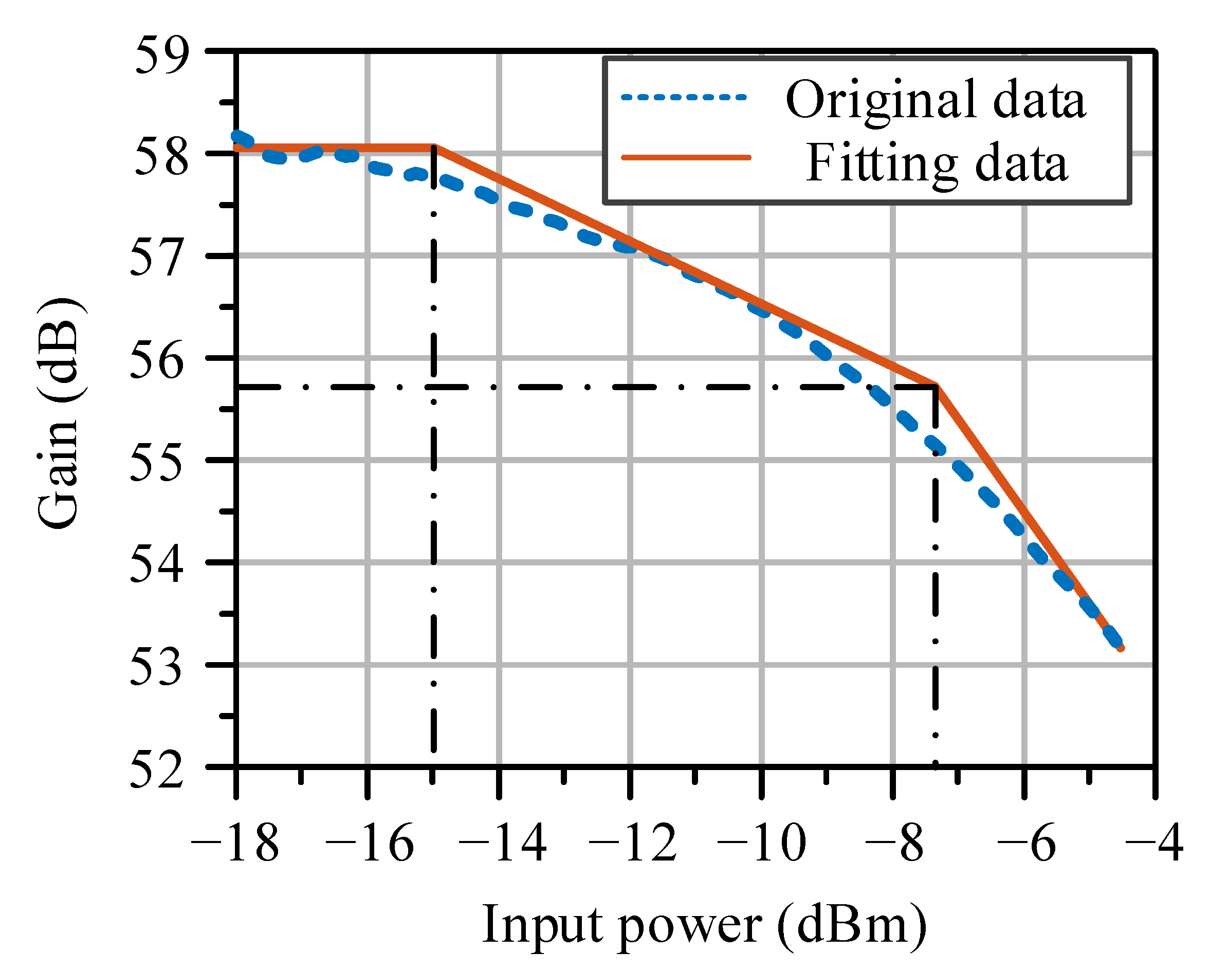
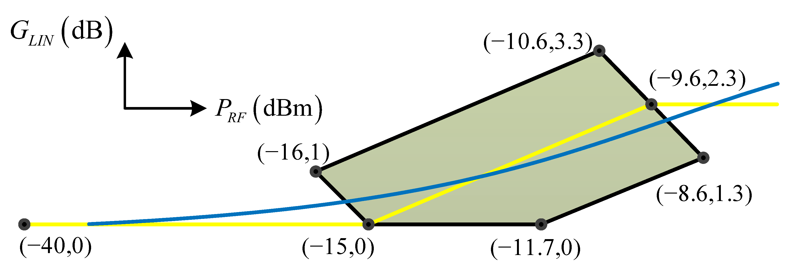
To verify the proposed method of design space expansion, a linearizer was designed and simulated for a millimeter-wave PA with a saturation power of 65 W operating from 40 to 43 GHz. The gain and phase characteristics of the PA are detailed in Figure 9, and the small-signal phase was normalized to 0. The gain characteristics of the PA were first fitted in three segments using the method presented in Section 2.1. As an example, the gain characteristics of the PA at a frequency of 40 GHz were fitted to the three segments, as shown in Figure 10, with the key parameters of the fitting curves obtained as follows: of 58 dB, of −15 dBm, of −7.3 dBm, and a gain compression slope of −0.3. The expanded gain design space was derived according to the key parameters and Figure 8, and is shown in the green area of Figure 11. The design space analyses and calculations for the phase characteristics were the same as for the gain characteristics.

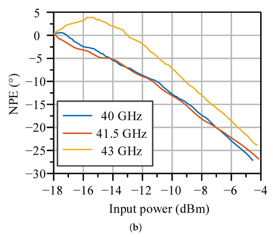
Figure 9.
(a) Gain characteristics and (b) normalized phase error (NPE) of the PA.
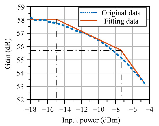
Figure 10.
Original and fitted gain characteristics of the PA at a frequency of 40 GHz.

Figure 11.
Gain design space (green area) and measured gain curve (blue line) of the linearizer at 40 GHz.
Then, a diode-based linearizer was designed while ensuring that its gain curve fell within the extended design space, as shown in Figure 11. A -type network was chosen to design the linearizer [19]. The series microstrip line of the -type network was replaced with four-stage cascading microstrip lines to obtain multiple amplitude and phase characteristics, and the bias voltage, resistor, and network parameters were tuned such that the gain curve of the linearizer fell within the design space.
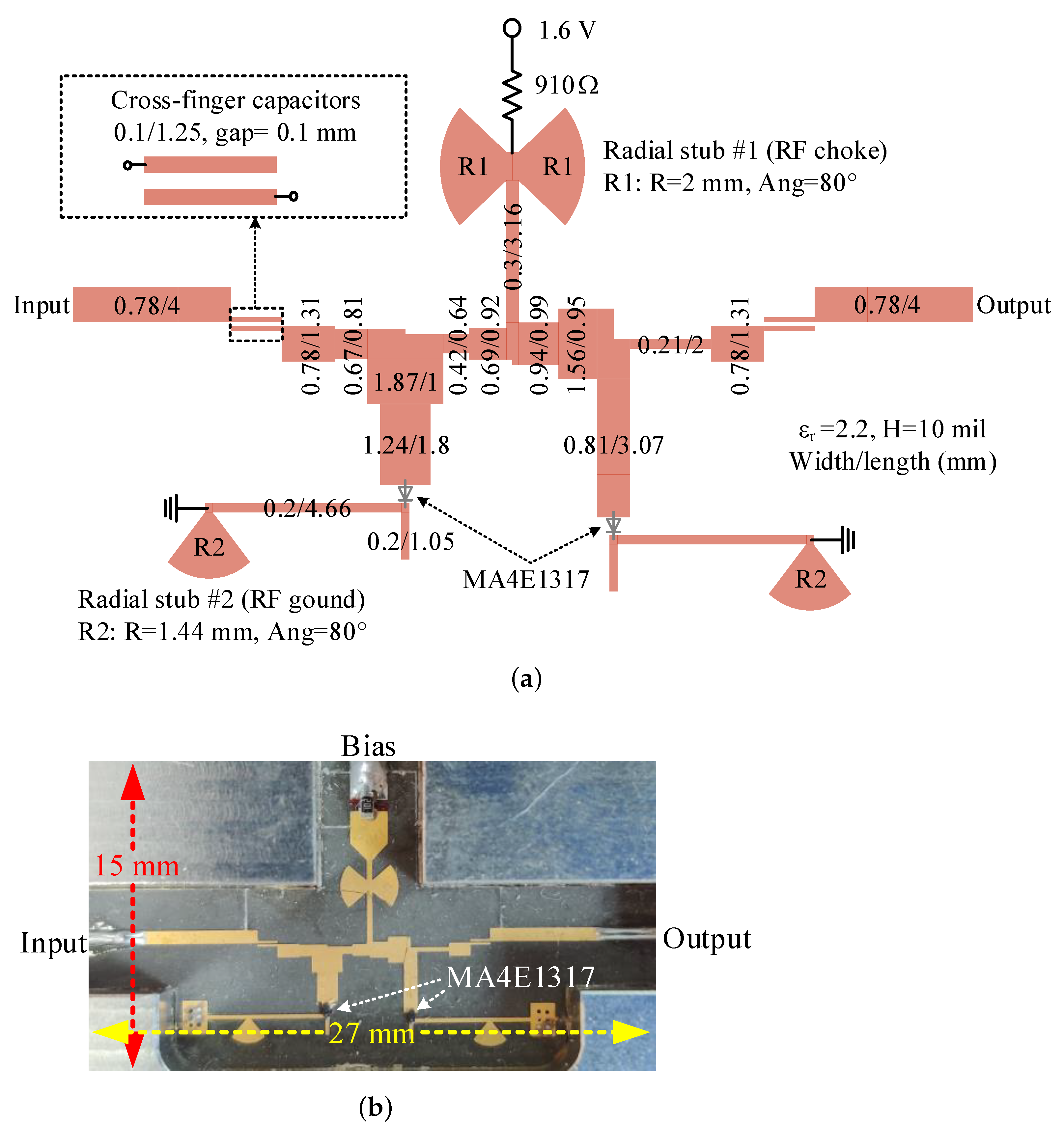
The layout of the proposed linearizer is shown in Figure 12a. An MA4E1317 millimeter-wave Schottky diode produced by MACOM was used was, and the substrate was a Rogers RT/duroid 5880 ( = 2.2, H = 10 mil). The first radial stub had a radius of half a wavelength, allowing for use as an RF choke, and the second radial stub with a half-wavelength line was used to short the RF signal, which can reduce the inductance effect in comparison with bias to the ground. The DC block of the input and output was realized using microstrip cross-finger capacitors with an insertion loss of less than 0.1 dB.

Figure 12.
(a) Layout of the proposed linearizer and (b) photograph of the fabricated linearizer.
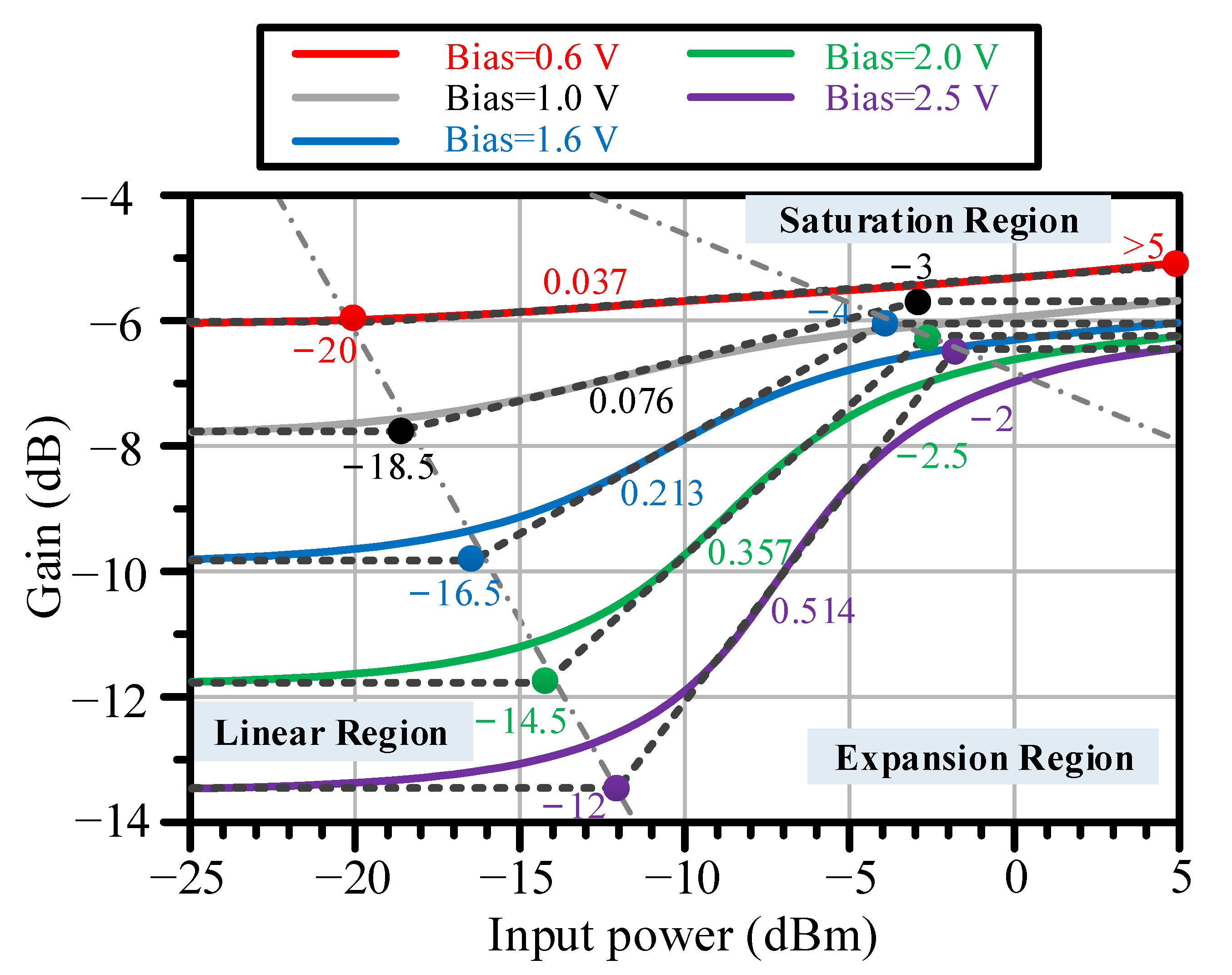
The simulation results for the linearizer at 40 GHz with different bias voltages are provided in Figure 13. Differently colored lines and text correspond to different bias voltages, and the bias resistor was fixed to 910 . The gain characteristics at the gain expansion turn-on and turn-off points of the linearizer with different biases are shown in Figure 13 in three separate regions. According to the previous analysis, the linearizer design focused on the turn-on points and expansion regions, as shown in Figure 13. From the line of the turn-on points (i.e., the dividing line between the linear region and expansion region), as shown in Figure 13, it was calculated that the linearizer had similar gain expansion turn-on output power (i.e., ) when the network parameters were determined and that the bias mainly affected the expansion slope.

Figure 13.
Simulation results for the proposed linearizer at 40 GHz with different bias voltages.
Comparing the design space shown in Figure 11 with that shown in Figure 13, it should be noted that the minimum gain of the linearizer in Figure 11 was assumed to be 0 dB in order to simplify the analysis. The gain shown in Figure 13 was achieved by cascading a small-signal amplifier after the linearizer to realize a small-signal gain of 0 dB. The ideal linearizer function obtained with (3) corresponded to a gain curve with a bias of 2 V, as shown in Figure 13. However, when using the extended design space shown in Figure 8 to calculate the linearizer design space for 41.5 GHz and 43 GHz, the linearizer was unable to achieve the preset linearization goal at 43 GHz and a bias of 2 V. Considering the design space of multiple frequencies and the configuration of the small-signal amplifier, a bias of 1.6 V was finally chosen to implement the proposed linearizer.
4. Measurements and Results
4.1. Measurement Platform
The proposed linearizer was fabricated and tested at 40 GHz, 41.5 GHz, and 43 GHz. A photograph of the fabricated circuit is shown in Figure 12b. The measurement platform used in this study was previously introduced, and the schematic of the linearization platform is shown in Figure 14. A continuous-wave test and two-tone signal test were both performed with the N5247A network analyzer from Keysight. The broadband signal excitation could not be tested due to platform limitations.
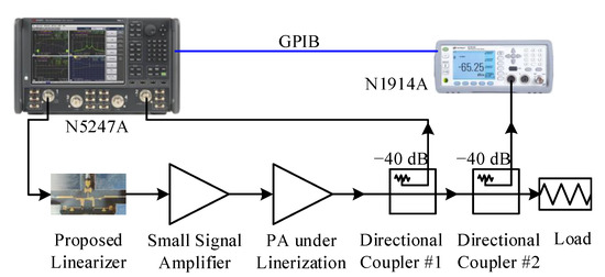
Figure 14.
Schematic of the linearization platform.
An AMMC-5040 small-signal amplifier from Broadcom was used to compensate for the insertion loss of the linearizer, ensuring that the gain of the linearizer was greater than 0 dB within its operating power. This allowed the cascaded linearizer–PA system to maintain the preset output dynamic range without the input dynamic range being extended due to the loss introduced by the linearizer. The bias voltage and current of the AMMC-5040 were 4 V and 150 mA, respectively. The bias current of the linearizer was about 1 mA, and the total power consumption of the proposed linearizer with non-negative gain within the operating power was about 0.6 W.
The output of the PA was fed into a directional coupler with a coupling of −40 dB, with the coupled signal used as the reception signal for the N5247A. Another directional coupler with a coupling of −40 dB was used to couple the signal to an N1914A power meter from Keysight for power calibration. The N5247A and N1914A were connected and interactively controlled using GPIB. A load was utilized for power collection. Because the proposed linearizer does not need to regulate the power supply for testing at broadband frequencies, not all of power supplies in the measurement platform are provided here.
4.2. Continuous-Wave Test
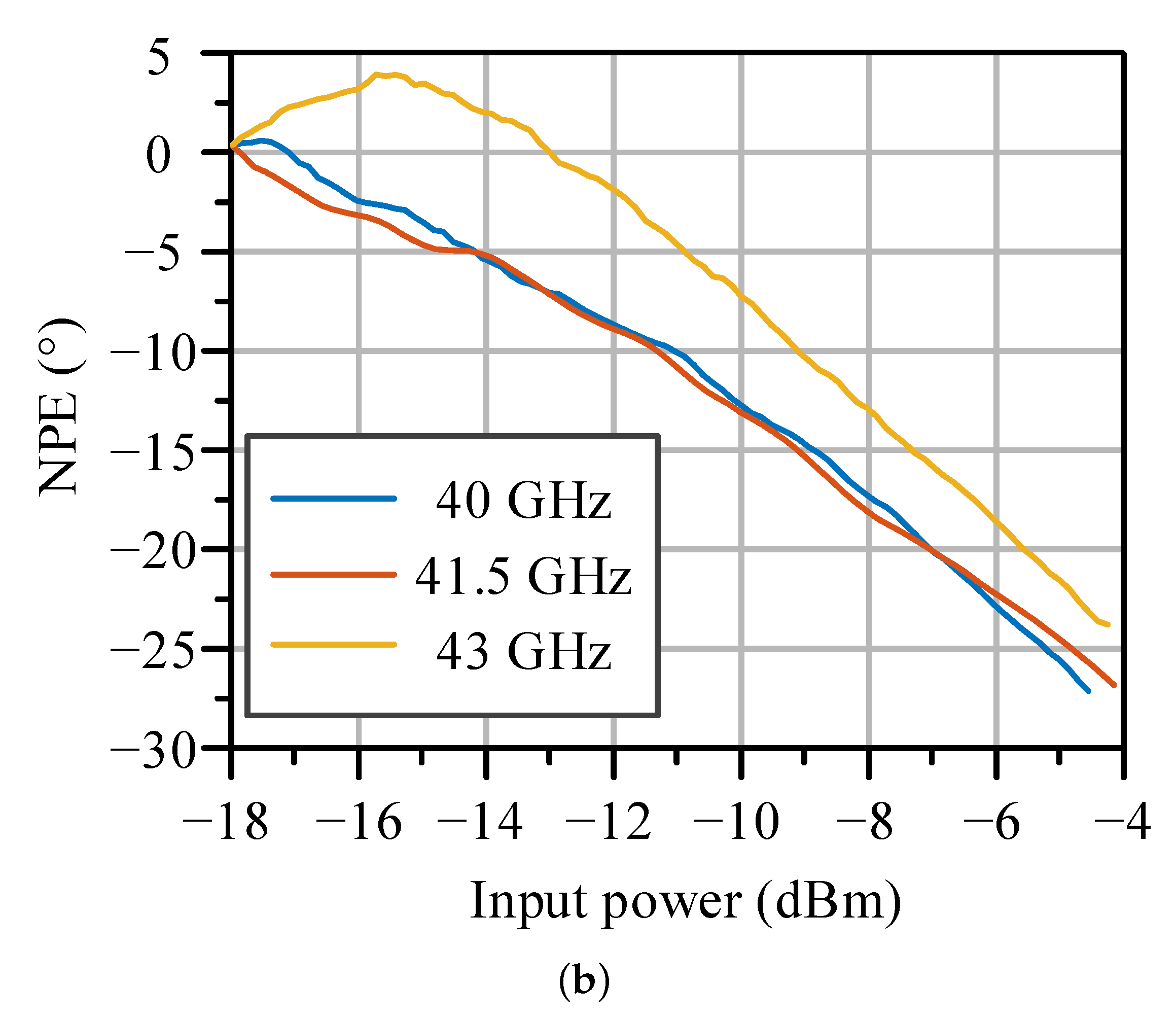
The proposed linearizer was first tested with a continuous wave. The scanning power of the N5247A was set from −20 dBm to 0 dBm at 40 GHz, 41.5 GHz, and 43 GHz. The measured gain and NPE characteristics of the linearizer are detailed in Figure 15. The MA4E1317, which had a bias of 1.6 V and 910 , offered a phase compensation of about 30 over the frequency range. The gain curve of the linearizer at 40 GHz is shown in Figure 11 for comparison; the minimum gain of the linearizer was greater than 0 dB when the small-signal amplifier was added, and it can be seen that the gain curve fell within the design space (green) and achieved the preset linearization goal.
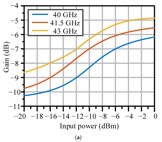
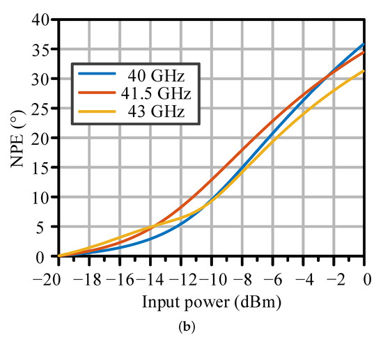
Figure 15.
(a) Measured gain characteristics of the linearizer and (b) measured phase characteristics of the linearizer.
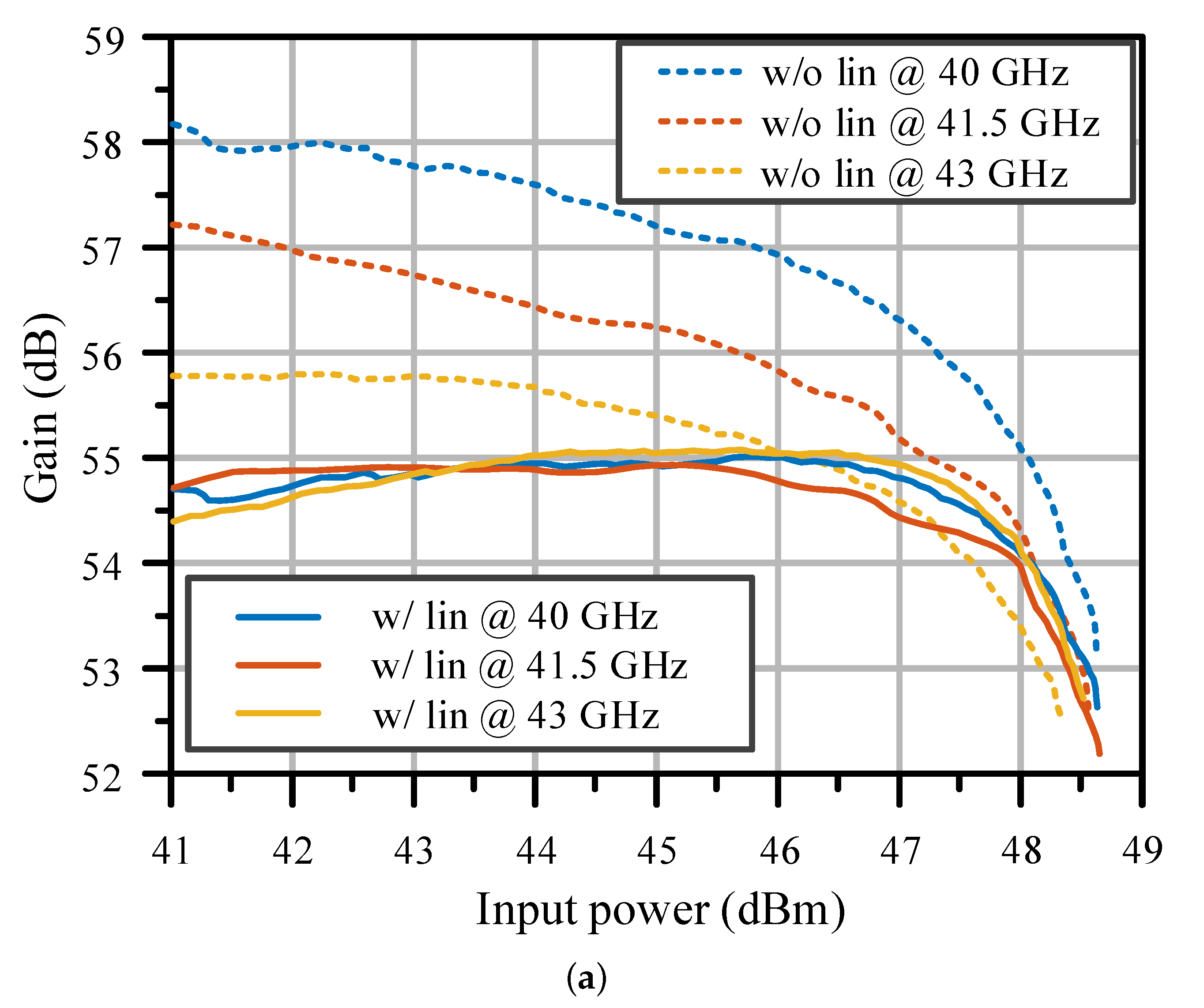
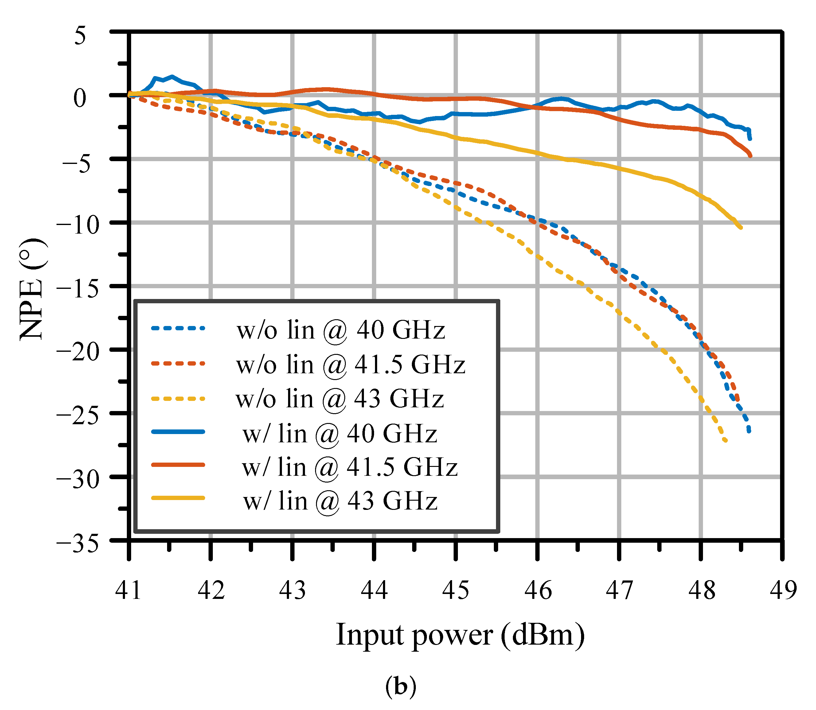
Next, the cascaded linearizer–PA was tested under the same conditions. The measured gain characteristics of the linearized PA are detailed in Figure 16. It can be seen in Figure 16a that the linearized PA had a gain fluctuation of less than 1 dB compared with the small-signal gain before the output power of 48 dBm, while the output 1 dB power point () and the NPE were improved by more than 1.7 dB and 15 at the power of 48 dBm over the operating frequency range, respectively.

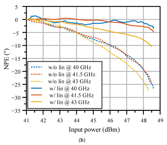
Figure 16.
(a) Measured gain characteristics of the linearized PA and (b) measured phase characteristics of the linearized PA.
4.3. Two-Tone Signal Test
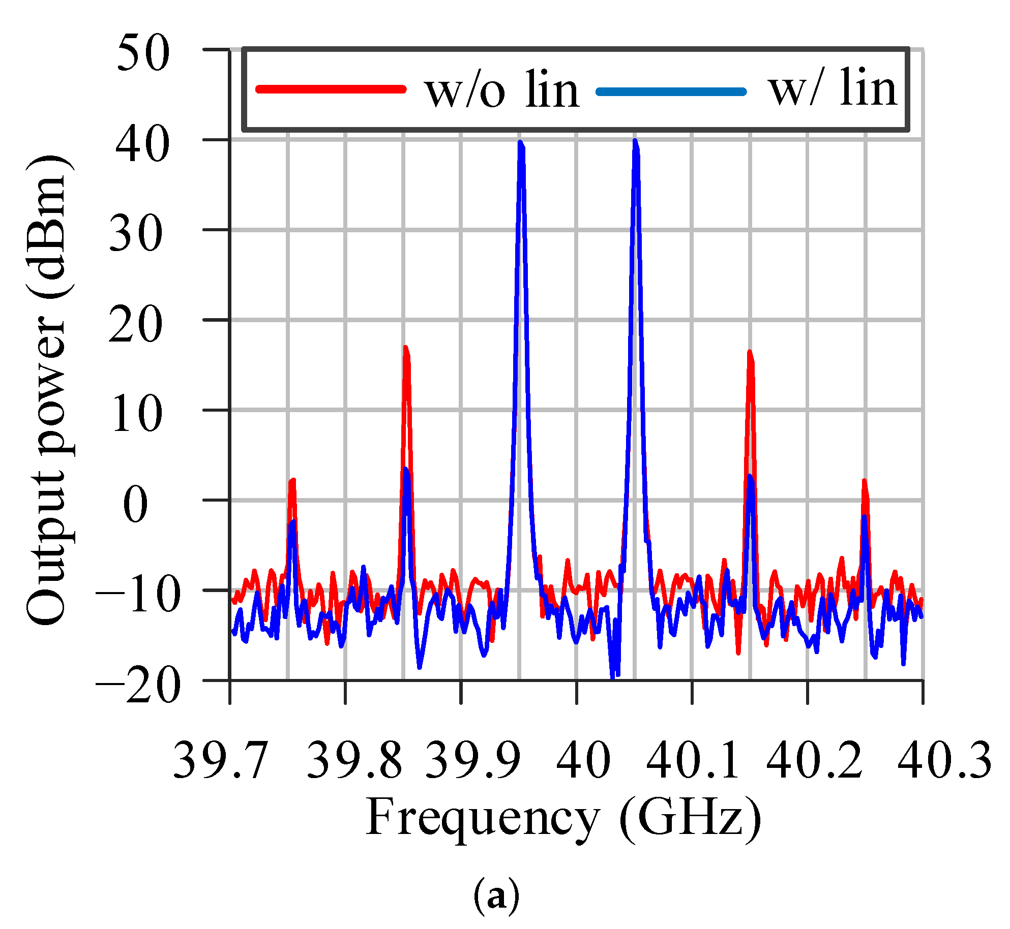
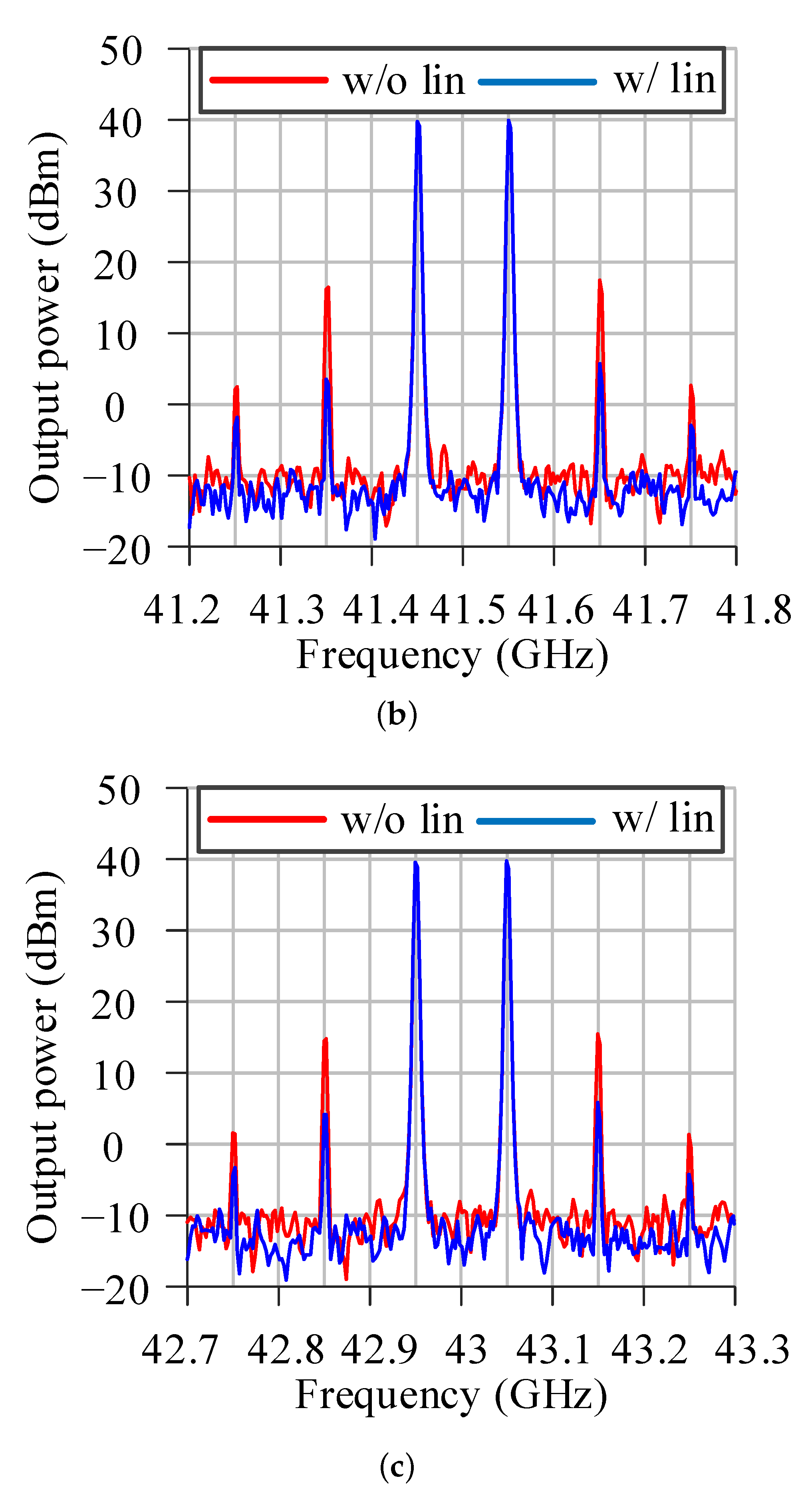
Then, the linearized PA was tested with a two-tone signal with a spacing of 100 MHz. The total output power of the PA was fixed at a 6 dB output back-off (OPBO). The third-order intermodulation distortion (IMD3) of the PA with and without the linearizer at the center frequencies of 40 GHz, 41.5 GHz, and 43 GHz was measured, with the results shown in Figure 17. The IMD3 was suppressed by more than 13.1 dB, 10.5 dB, and 8.6 dB, respectively, at these frequencies. All of the experimental results are summarized in Table 1.

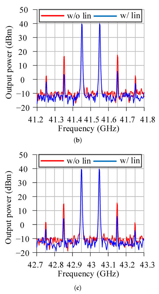
Figure 17.
Spectra of the two-tone signal output with and without the linearizer at a center frequency of (a) 40 GHz, (b) 41.5 GHz, and (c) 43 GHz.

Table 1.
Experimental results.
The proposed broadband linearizer based on an extended design space was designed to achieve good linearization over the entire working frequency without bias tuning. A comparison between selected diode-based broadband linearizers and the one proposed in this work is presented in Table 2. The IMD3 suppression values in the table were all measured at 6 dB OPBP. The proposed linearizer achieved IMD3 suppression values of 8.6 dB–13.1 dB with a 100 MHz two-tone signal at 6 dB OPBO from 40 GHz to 43 GHz. A comparison between recent diode-based linearizers and the one proposed in this work is presented in Table 2. Considering the linearization performance, power consumption, working bandwidth, and design complexity, the proposed linearizer is comparable to the state of the art.
Table 2.
Comparison with recent diode-based linearizers.
5. Conclusions
In this study, a broadband linearizer based on an extended design space is proposed and analyzed. The definition of the 1 dB power point greatly extends the design space of the linearizer, and the three-segment fitting curves further simplify the analysis and computation of the design space. To verify the proposed method, a linearizer prototype was fabricated and tested from 40 GHz to 43 GHz. The measurement results of the linearized PA showed that the value was improved by more than 1.7 dB, the phase error was reduced by more than 15, and the IMD3 was suppressed by 8.6 dB–13.1 dB over the working frequency range. The proposed linearizer achieved good linearization performance, low power consumption, and simple design implementation, and there was no need to tune the bias during broadband operation, making it applicable to complex communication scenarios.
Author Contributions
Conceptualization, P.H. and C.S.; methodology, P.H.; validation, P.H., M.S., P.W. and C.S.; investigation, P.H.; writing—original draft preparation, P.H. and M.S.; writing—review and editing, P.H. All authors have read and agreed to the published version of the manuscript.
Funding
This work was supported in part by the National Natural Science Foundation of China under Grants 62271114, 62101077, and 61871075, in part by the Science and Technology Special Program of Huzhou under Grant 2022YZ45, and in part by the Scientific Research Foundation for the Yangtze Delta Region Institute (Huzhou) of the University of Electronic Science and Technology of China under Grant U03220082.
Data Availability Statement
The data that support the findings of this study are available within the article.
Conflicts of Interest
The authors declare no conflicts of interest.
References
- Xiao, M.; Mumtaz, S.; Huang, Y.; Dai, L.; Li, Y.; Matthaiou, M.; Karagiannidis, G.K.; Björnson, E.; Yang, K.; Chih-Lin, I.; et al. Millimeter wave communications for future mobile networks. IEEE J. Sel. Areas Commun. 2017, 35, 1909–1935. [Google Scholar] [CrossRef]
- Niu, Y.; Li, Y.; Jin, D.; Su, L.; Vasilakos, A.V. A survey of millimeter wave communications (mmWave) for 5G: Opportunities and challenges. Wirel. Netw. 2015, 21, 2657–2676. [Google Scholar] [CrossRef]
- Park, B.; Jin, S.; Jeong, D.; Kim, J.; Cho, Y.; Moon, K.; Kim, B. Highly linear mm-wave CMOS power amplifier. IEEE Trans. Microw. Theory Tech. 2016, 64, 4535–4544. [Google Scholar] [CrossRef]
- Yu, C.; Jing, J.; Shao, H.; Jiang, Z.H.; Yan, P.; Zhu, X.W.; Hong, W.; Zhu, A. Full-angle digital predistortion of 5G millimeter-wave massive MIMO transmitters. IEEE Trans. Microw. Theory Tech. 2019, 67, 2847–2860. [Google Scholar] [CrossRef]
- Haider, M.F.; You, F.; He, S.; Rahkonen, T.; Aikio, J.P. Predistortion-based linearization for 5G and beyond millimeter-wave transceiver systems: A comprehensive survey. IEEE Commun. Surv. Tutor. 2022, 24, 2029–2072. [Google Scholar] [CrossRef]
- Katz, A.; Wood, J.; Chokola, D. The Evolution of PA Linearization: From Classic Feedforward and Feedback Through Analog and Digital Predistortion. IEEE Microw. Mag. 2016, 17, 32–40. [Google Scholar] [CrossRef]
- Zhang, H.; Sanchez-Sinencio, E. Linearization Techniques for CMOS Low Noise Amplifiers: A Tutorial. IEEE Trans. Circuits Syst. 2011, 58, 22–36. [Google Scholar] [CrossRef]
- Peng, J.; You, F.; He, S. Under-sampling digital predistortion of power amplifier using multi-tone mixing feedback technique. IEEE Trans. Microw. Theory Tech. 2021, 70, 490–501. [Google Scholar] [CrossRef]
- Guan, L.; Zhu, A. Green communications: Digital predistortion for wideband RF power amplifiers. IEEE Microw. Mag. 2014, 15, 84–99. [Google Scholar] [CrossRef]
- Yu, C.; Guan, L.; Zhu, E.; Zhu, A. Band-limited Volterra series-based digital predistortion for wideband RF power amplifiers. IEEE Trans. Microw. Theory Tech. 2012, 60, 4198–4208. [Google Scholar] [CrossRef]
- Zhang, D.; Fu, W.; Deng, X.; Xu, X.; Zhang, B.; Yu, H.; Ma, K. X-to Q-Band MMIC Predistortion Linearizers with Tunable Frequency-Dependent Phase Conversion Capacity Using GaAs HEMT Technology. IEEE Trans. Microw. Theory Tech. 2022, 71, 1536–1549. [Google Scholar] [CrossRef]
- Xiao, Z.; You, F.; Hao, P.; Wang, Y.; He, Q.; Shen, C.; Li, C.; Ma, M.; Wu, J.; Fan, Y.; et al. A Ka-Band CMOS Power Amplifier with OP1dB Improvement Employing a Diode-Connected Analog Linearizer. IEEE Trans. Circuits Syst. Express Briefs 2023, 70, 2271–2275. [Google Scholar] [CrossRef]
- Deng, H.; Zhang, D.; Lv, D.; Zhou, D.; Zhang, Y. Analog Predistortion Linearizer with Independently Tunable Gain and Phase Conversions for Ka-band TWTA. IEEE Trans. Electron Devices 2019, 66, 1533–1539. [Google Scholar] [CrossRef]
- Yamauchi, K.; Mori, K.; Nakayama, M.; Mitsui, Y.; Takagi, T. A microwave miniaturized linearizer using a parallel diode with a bias feed resistance. IEEE Trans. Microw. Theory Tech. 1997, 45, 2431–2435. [Google Scholar] [CrossRef]
- Zhu, R.; Zhang, X.; Shen, D.; Zhang, Y. Ultra Broadband Predistortion Circuit for Radio-over-Fiber Transmission Systems. J. Lightw. Technol. 2016, 34, 5137–5145. [Google Scholar] [CrossRef]
- Rezaei, S.; Hashmi, M.S.; Dehlaghi, B.; Ghannouchi, F.M. A systematic methodology to design analog predistortion linearizer for dual inflection power amplifiers. In Proceedings of the 2011 IEEE MTT-S International Microwave Symposium, Baltimore, MD, USA, 5–10 June 2011; pp. 1–4. [Google Scholar] [CrossRef]
- Gumber, K.; Rawat, M. Low-Cost RFin–RFout Predistorter Linearizer for High-Power Amplifiers and Ultra-Wideband Signals. IEEE Trans. Instrum. Meas. 2018, 67, 2069–2081. [Google Scholar] [CrossRef]
- Gumber, K.; Rawat, M. Analogue predistortion lineariser control schemes for ultra-broadband signal transmission in 5G transmitters. IET Microwaves Antennas Propag. 2020, 14, 718–727. [Google Scholar] [CrossRef]
- Hao, P.; He, S.; You, F.; Shi, W.; Peng, J.; Li, C. Independently tunable linearizer based on characteristic self-compensation of amplitude and phase. IEEE Access 2019, 7, 131188–131200. [Google Scholar] [CrossRef]
- Tang, H.; He, S.; Hao, P.; Song, M.; Guo, J.; Xiao, Z.; Zhang, X.; Zeng, S.; Liu, Y.; Zhang, X.; et al. A Design Method for Reflective Analog Predistorter with Independently Tunable Gain. IEEE Microw. Wirel. Technol. Lett. 2024, 34, 338–341. [Google Scholar] [CrossRef]
- Song, M.; He, S.; You, F.; Zhang, X.; Zhong, C.; Yin, Y.; Xiao, Z.; Tang, H.; Guo, J.; Hao, P. An Analog Predistorter for Doherty Power Amplifiers Based On Minimum Gain and Phase Deviation. IEEE Trans. Circuits Syst. Express Briefs, 2024; early access. [Google Scholar]
- Kao, K.Y.; Hsu, Y.C.; Chen, K.W.; Lin, K.Y. Phase-Delay Cold-FET Pre-Distortion Linearizer for Millimeter-Wave CMOS Power Amplifiers. IEEE Trans. Microw. Theory Tech. 2013, 61, 4505–4519. [Google Scholar] [CrossRef]
- Cripps, S.C. RF Power Amplifiers for Wireless Communications; Artech house Norwood: Norwood, MA, USA, 2006; Volume 250. [Google Scholar]
- Belluot, J.; Rhun, G.L.; Augoyat, P.; Mouchon, G.; Maati, A.; Katz, A.; Gray, B.; Dorval, R. A 40 W Ka-Band RF Amplification Chain for Space Telecommunication SSPA Applications. In Proceedings of the 2019 49th European Microwave Conference (EuMC), Paris, France, 1–3 October 2019; pp. 404–407. [Google Scholar] [CrossRef]
- Yang, Y.; Chen, W.; Feng, Z. A Broadband Analog Predistortion Linearizer Based on Tunable Diodes for Ka Band Power Amplifier. In Proceedings of the 2020 International Conference on Microwave and Millimeter Wave Technology (ICMMT), Shanghai, China, 17–20 May 2020; pp. 1–3. [Google Scholar] [CrossRef]
- Hao, P.; He, S.; You, F.; Ge, J. Broadband linearizer based on equivalent power-dependent impedance function of diode and load match network. Microw. Opt. Technol. Lett. 2021, 63, 499–503. [Google Scholar] [CrossRef]
- Liu, T.; Su, X.; Wang, G.; Zhao, B.; Fu, R.; Zhu, D. A Broadband Analog Predistortion Linearizer Based on GaAs MMIC for Ka-Band TWTAs. Electronics 2023, 12, 1503. [Google Scholar] [CrossRef]


Disclaimer/Publisher’s Note: The statements, opinions and data contained in all publications are solely those of the individual author(s) and contributor(s) and not of MDPI and/or the editor(s). MDPI and/or the editor(s) disclaim responsibility for any injury to people or property resulting from any ideas, methods, instructions or products referred to in the content. |
© 2024 by the authors. Licensee MDPI, Basel, Switzerland. This article is an open access article distributed under the terms and conditions of the Creative Commons Attribution (CC BY) license (https://creativecommons.org/licenses/by/4.0/).