Article

A Robust CCS Predictive Current Control for Photovoltaic Energy Storage System Based on a Nonlinear Disturbance Observer

School of Electrical Engineering, Xi’an University of Technology, Xi’an 710048, China
*
Author to whom correspondence should be addressed.
Electronics 2023, 12(9), 1985; https://doi.org/10.3390/electronics12091985
Submission received: 22 March 2023 / Revised: 20 April 2023 / Accepted: 21 April 2023 / Published: 24 April 2023
(This article belongs to the Special Issue System Integration of Renewable Energy Generation)

Abstract

:
This article introduces a new control strategy for a bidirectional DC/DC converter used in photovoltaic energy storage systems (PV-ESSs), aimed to address the DC bus voltage deviation problem. The purpose of this paper is to design and practically implement a robust continuous control set predictive current control (CCS-PCC) method based on a nonlinear disturbance observer (NDO) to tightly regulate the common DC bus voltage in islanded DC microgrids. The CCS-PCC controller is used to replace the current loop PI controller, which effectively overcomes the shortcomings of the traditional linear lag control and improves the dynamic performance of the system. At the same time, the CCS-PCC method solves the inherent defect of finite control set predictive current control (FCS-PCC), where the switching frequency is not fixed. It effectively reduces the current ripple and realizes constant frequency control. In order to effectively suppress the DC bus voltage fluctuation during transients, the nonlinear disturbance observer is designed and combined with CCS-PCC. The feedforward method based on the NDO was utilized to enhance the disturbance rejection capability of the system. The simulation and experimental results show the feasibility and effectiveness of the proposed CCS-PCC+NDO approach, both during transient and steady-state operating conditions.

1. Introduction

Due to the depletion of fossil fuels and the aggravation of environmental pollution, the effective development and utilization of renewable energy sources has gained tremendous attention. As most of the distributed sources (e.g., PV, fuel cells, energy storage systems, etc.) are DC power and there is growing penetration of DC loads into microgrids, DC microgrids are becoming more and more attractive [1]. Compared with AC microgrids, DC bus voltage is the only measure of system power balance. DC microgrids have the advantage of being easy to control and do not have problems with frequency stability, synchronization, reactive power balance and harmonics. In recent years, DC microgrids have been widely used in different fields, such as renewable energy systems [2], data centers, electric vehicles [3], etc. Despite the aforementioned advantages of DC microgrids, there are various challenges that need to be addressed, especially in islanded DC microgrids.
Maintaining the stability of DC bus voltage is the critical control task in DC microgrids. The changes of photovoltaic output power, load mutations and the usage of a great number of power electric converters may make the DC bus voltage fluctuate [4]. Especially in islanded DC microgrids, the microgrids not only provide power balance but also supply load current. Therefore, large DC bus voltage fluctuations are not acceptable for many applications where there are sensitive DC loads connected to the DC link [5]. In order to ensure the stable operation of the system, transient DC bus voltage control is especially critical.
Ref. [6] introduces a mode-adaptive decentralized control scheme that improves the classical droop method. Despite the advantages of facilitating flexible mode definition, seamless mode transition and reliable power-sharing, the proposed energy management method cannot offer tight regulation of the common DC bus voltage. In order to address the inherent shortcomings of linear droop control, a nonlinear control method is proposed to improve voltage regulation and the load current-sharing accuracy in [7]. Three novel nonlinear droop control schemes are analyzed and implemented to adaptively adjust the droop gains. In the above papers, although the DC bus voltage fluctuations are suppressed from the perspective of energy management, the suppression effect of transient fluctuations is unsatisfactory.
Power electronic converters are the main building blocks in microgrids for renewable energy sources (RESs) and ESSs. The bidirectional DC/DC converter is a bridge connecting renewable energy sources and the energy storage medium. It provides power control and voltage and current regulation to ensure stable, reliable and efficient operation of DC microgrids [8]. The various disturbance problems in PV-ESSs can be solved through the improvement of converter topology and control strategy of the bidirectional DC/DC converter. In [9], a novel bidirectional isolated DC/DC converter with high voltage gain and wide input voltage is proposed, which can improve the efficiency of the converter, reduce the voltage surges on switches, and have the characteristics of zero voltage switching on certain switches. Several studies have been conducted on bidirectional DC/DC converter topology, especially focusing on the utilization of soft switching technology [10,11,12]. In [13], it is proved by theoretic analysis that the traditional double closed-loop PI control method cannot guarantee system stability under all conditions, and an improved theoretical control method is proposed. The current controller for a bidirectional hybrid DC/DC converter in [14] is designed by using the Bode-based frequency domain, where simulation and experimental results indicate that the reference current can be tracked well by using the control method with good dynamic stability. Although the proposed method offers several improvements, the characteristic of the traditional linear lag control limits the improvement of the system’s dynamic performance.
In order to overcome the disadvantages of the linear control method, some advanced nonlinear control methods—such as sliding mode control [15,16], passivity-based control [17] and backstepping control [18]—have been proposed to improve the dynamic performance and stability of the system. However, most of these nonlinear control methods fall under lag control. As a powerful technique for optimized performance tracking, model predictive control (MPC) has attracted great attention in recent years [19]. MPC is a kind of lead control method that uses a dynamic model of the system to predict its future response and has the advantages of fast dynamic response and simple design. It has been used widely in the fields of motor control [20,21,22], aircraft [23] and power converters [24,25,26,27,28,29,30,31,32,33,34,35]. In [26], a control method of a five-level grid-connected photovoltaic inverter based on the model predictive control is applied for controlling active and reactive powers injected into the grid. In [27], the model predictive control is used to improve the performance of pre-compensated power supplies, and the output voltage reference can be modified dynamically. In [28], a novel TS fuzzy-based adaptive MPC controller is proposed to modify the ESS current according to the changes in the CPL power included in a DC microgrid. This method can improve the dynamic performance and disturbance rejection capability of the system. A robust predictive current control for a photovoltaic energy storage system based on a second-order tracking differentiator (STD) is proposed in [29]. Ref. [31] proposed an improved model predictive control method using optimized voltage vectors and switching sequences. Compared with FSF-MPC, the improved MPC method can significantly reduce the switching loss. The article [32] introduces a general ANN-MPC approach to address the computational challenge of adopting MPC in highly complex power converters. In [33], a model predictive control method with autotuning weighting factor capability is presented. The proposed MPC method simplifies the controller design considerably. In [34], a dual-layer model predictive control method is proposed to control the charging/discharging behaviors efficiently. Considering the above analysis, the dynamic performance and robustness of the system are improved by using this lead control method. However, most of the presented MPC controls focus on the finite control set MPC.
In addition, an accurate system model is required to achieve high-precision tracking performance, which is always hindered by system uncertainties and external disturbances in real situations. Combining MPC with a disturbance observation/compensation process is a possible solution [36,37]. In [36], a voltage-current double closed-loop and power feedforward control method is proposed in a DC/DC converter. In [37], an MPC controller integrating with a nonlinear disturbance observer is proposed for a buck converter, aiming to realize accurate voltage tracking. However, this method is not verified in the bidirectional DC/DC converter.
In this article, a robust continuous control set predictive current control (CCS-PCC) method is proposed, which is able to enhance the dynamic response of the closed-loop control system against transients, tightly regulate the DC bus voltage and provide high-stability margins against the different loads. At the same time, the CCS-PCC method can reduce the current ripple effectively and realize constant frequency control. Compared with FCS-PCC, the proposed control method can reduce the current ripple in boost model and buck mode by 77.3% and 75%. Meanwhile, a nonlinear disturbance observer is designed and combined with CCS-PCC to improve the disturbance rejection capability of the DC-bus, especially in transients, which can track the equivalent load current quickly in the system without adding any extra current sensors. The uncertainties and disturbance items can be checked and compensated directly to the current loop. The DC bus voltage fluctuations can be suppressed effectively by feedforward compensation, and the system dynamic performance is further improved.
This paper is organized as follows: the structure of a typical islanded DC microgrid is described and the mathematical model of the bidirectional DC/DC converter is established in Section 2. In Section 3 the proposed control strategy is presented. The design of the CCS-PCC controller in different operation modes is presented. The NDO-based voltage loop feedforward principle is analyzed. The design process of NDO is given and the stability analysis is also performed in this section. The correctness and effectiveness of the proposed method are verified by the simulation and experimental results in section IV and section V, respectively. Finally, a conclusion ends this paper.

2. System Structure and Modeling

A typical islanded DC microgrid with various sources and loads is shown in Figure 1. The system consists of PV power generation units, energy storage systems (ESSs), power electronic converters and different kinds of loads.
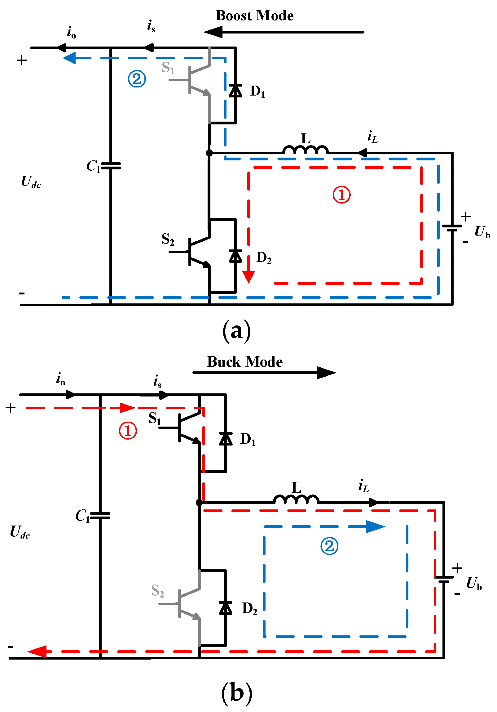
It can be seen from Figure 1 that the ESS in the system is connected to the DC bus through the bidirectional converter. This paper mainly focuses on how to keep the DC bus voltage constant through the energy storage converter control strategy improvement. The operational principle of the bidirectional DC/DC converter is shown in Figure 2. Udc represents the DC bus voltage, C1 represents the support capacitor of the high voltage side, L represents the energy storage inductor, Ub represents the batteries’ terminal voltage, is is the output current of the DC bus side, and iL and io represent the inductor current and the equivalent load current, respectively. d1 and d2 represent the switching state of S1 and S2, respectively (di = 1 represents switch Si turns on, di = 0 represents switch Si turns off, i = 1, 2).

2.1. Boost Mode

Boost mode occurs when the power load required is greater than the PV output power. The power is delivered from the batteries (ESSs) to the DC side and the batteries discharge by ESSs. The bidirectional DC/DC converter works in boost mode (see Figure 2a).
Stage ①: When d2 = 1, switch tube S1 is off, switch tube S2 is on. The batteries discharge through L and S2, inductor L storage energy. Capacitor C1 supplies energy to loads.
{ L d i L d t = U b C 1 d U d c d t = i o .
Stage ②: When d2 = 0, switch tube S1 is off, switch tube S2 is off. The battery and inductor L charge for the capacitor C1 and provide energy to the loads with PV together.
{ L d i L d t = U b U d c C 1 d U d c d t = i L i o .
According to the above analysis, the mathematical model of the bidirectional DC/DC converter in boost mode can be written as Equation (3):
{ L d i L d t = U b ( 1 d 2 ) U d c C 1 d U d c d t = ( 1 d 2 ) i L i o .

2.2. Buck Mode

When the power load required is less than the PV output power, the batteries are used to absorb excess energy and the bidirectional DC/DC converter works in buck mode. (See Figure 2b).
Stage ①: When d1 = 1, switch tube S1 is on, switch tube S2 is off. The current io flows from DC bus through S1 and L to the batteries. In this stage, the batteries are charged from the DC side and the excess energy is stored in batteries.
{ L d i L d t = U d c U b C 1 d U d c d t = i o i L .
Stage ②: When d1 = 0, switch tubes S1 and S2 are both off. The body diode D2 of S2 is conducted. The inductor current iL flows through L, batteries and the body diode D2. The loop current equations are established as follows:
{ L d i L d t = U b C 1 d U d c d t = i o .
According to the above analysis, the mathematical model of the bidirectional DC/DC converter in buck mode can be written as Equation (6):
{ L d i L d t = d 1 U d c U b C 1 d U d c d t = i o d 1 i L .

3. Continuous Control Set Predictive Current Control Based on Nonlinear Disturbance Observer

Predictive current control is a branch of model predictive control. The basic principle of predictive current control is that the current value at the next moment is predicted according to the system model and the system state, and then the control signal at the next moment is selected by optimizing the objective function. This is a direct active regulation rather than a passive feedback control. The system can track the reference value quickly and achieve the desired control effect. Predictive current control includes finite control set predictive current control (FCS-PCC) and continuous control set predictive current control (CCS-PCC).
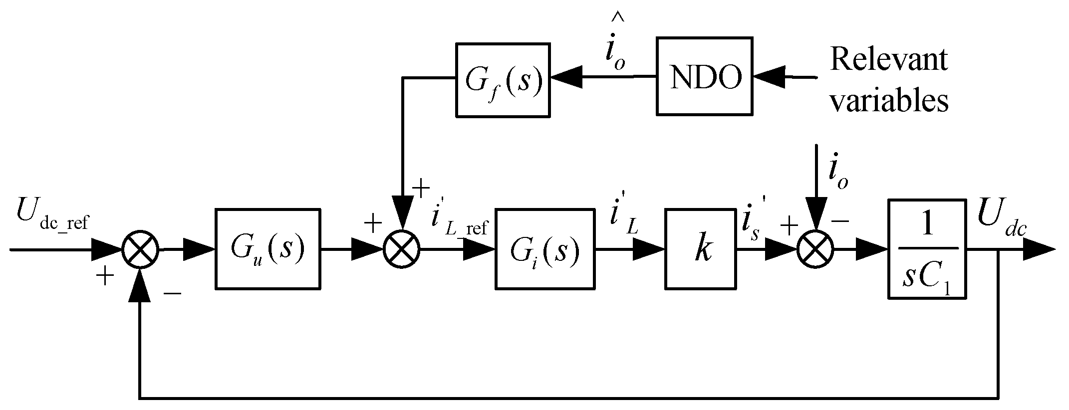
A robust CCS-PCC strategy for a bidirectional DC/DC converter based on a nonlinear disturbance observer (NDO) is proposed in this paper. The block diagram of the proposed control method is shown in Figure 3. Udc-ref represents the DC bus voltage reference, iL-ref represents the inductor current reference and i ^ o represents the observation value of the equivalent load current.
The CCS-PCC controller is used in the current loop. The traditional current loop controller based on PI is replaced. A PI controller is also used in the voltage loop controller. In order to effectively suppress the DC bus voltage fluctuation, especially in transients, the equivalent load current as the disturbance current can be tracked and estimated by the nonlinear disturbance observer. Compared to FCS-PCC, the proposed control method makes the switching frequency fixed, reduces the switch noise and improves the steady-state and dynamic performance.

3.1. Continuous Control Set Predictive Current Control Method

The control block diagram of the CCS-PCC controller proposed in this paper is shown in Figure 4. The inductor current prediction model is established by the mathematical expression of the inductor current of the bidirectional DC/DC converter. The reference value of the inductor current iL-ref is obtained from the voltage outer loop. For the bidirectional DC/DC converter, the measurable variables are the inductor current iL, the battery voltage Ub and the DC bus voltage Udc. The predictive value of the inductor current iL(k + 1) can be obtained by an inductor current predictive model. Then, the predictive value of the control variable is obtained according to the idea of deadbeat control. The predictive current model in different modes can be deduced according to the bidirectional DC/DC converter mathematical model.

3.1.1. The Design of CCS-PCC Controller in Boost Mode

When the bidirectional DC/DC converter operates in boost mode, assuming that the converter operates in a continuous conduction mode, the turn-on time of S2 is t1, and Ts represents the sampling time. The discrete expressions of Equation (1) can be described as follows:
L i L 0 ( k ) i L ( k ) t 1 = U b ( k ) .
where iL(k) is the inductor current value at the beginning of the time k, iL0(k) is the inductor current at the end of time k, and Ub(k) is the battery voltage value at time k.
Assuming that the turn-off time of S1 is t2 in a sampling control period, the discrete expressions of Equation (2) can be written as follows:
L i L ( k + 1 ) i L 0 ( k ) t 2 = U b ( k ) U d c ( k )
where iL(k + 1) is the inductor current value at the end of k time, which is also the inductor current at k + 1 time, Udc(k) is the DC bus voltage value at k time. Combining (7) with (8), we get:
L i L ( k + 1 ) i L ( k ) T s = U b ( k ) t 1 + [ U b ( k ) U d c ( k ) ] t 2 T s .
Defining
d boost = t 1 T s .
Substituting (10) into (9) yields:
i L ( k + 1 ) i L ( k ) = T s L [ U b ( k ) U d c ( k ) d boost U d c ( k ) ] .
According to the deadbeat idea, we can get:
i L ( k + 1 ) = i L _ ref .
Substituting (12) into (11) yields:
d boost = L T s i L _ ref   i L ( k ) U d c ( k ) U b ( k ) U d c ( k ) U d c ( k ) .
where dboost is the modulation wave of predictive current controller when the bidirectional DC/DC converter operates in boost mode.

3.1.2. The Design of CCS-PCC Controller in Buck Mode

When the bidirectional DC/DC converter operates in buck mode, we assume that the turn-on time of S1 is t3. The discrete expressions of Equation (4) can be described as follows:
L i L 0 ( k ) i L ( k ) t 3 = U d c ( k ) U b ( k ) .
Assuming that the turn-off time of S1 is t4 in a sampling period, the discrete expressions of Equation (5) can be written as follows:
L i L ( k + 1 ) i L 0 ( k ) t 4 = U b ( k ) .
Combining (14) with (15), we obtained:
L i L ( k + 1 ) i L ( k ) T s = [ U d c ( k ) U b ( k ) ] t 3 U b ( k ) t 4 T s .
Defining
d buck = t 3 T s .
Substituting (17) into (16) yields:
i L ( k + 1 ) i L ( k ) = T s L [ d buck U d c ( k ) U b ( k ) ] .
According to the deadbeat idea, we can get:
d buck = L T s i L _ ref i L ( k ) U d c ( k ) + U b ( k ) U d c ( k ) .
where dbuck is the modulation wave of predictive current controller when the bidirectional DC/DC converter operates in buck mode.

3.2. Analysis of DC Bus Voltage Based on NDO

According to the previous analysis, the DC bus voltage equation of the system can be obtained as follows:
{ C 1 d U d c d t = i s i o U b i L = U d c i s .
The voltage and current double closed loop control structure is adopted, in which the voltage loop is a PI controller and the current loop is a CCS-PCC controller. The usual DC bus voltage control structure [38] is shown in Figure 5.
According to the block diagram in Figure 5, the relationship of Udc-ref, Udc and io is established as follows:
U d c   ( s ) = 1 s C 1 k G u ( s ) G i ( s ) 1 + 1 s C 1 k G u ( s ) G i ( s ) U d c _ ref   ( s ) 1 s C 1 + k G u ( s ) G i ( s ) i o ( s ) .
where Gu(s) is the transfer function of the voltage loop PI controller, Gi(s) is the transfer function of the current loop CCS-PCC controller (the transfer function of the CCS-PCC controller is one in ideal condition), and k = Ub/Udc is the conversion gain, which is derived from Equation (20).
According to the Formula (21), the DC bus voltage of the system is not only related to Udc-ref, but also is affected by the equivalent load current io. The power disturbance of the DC bus side, such as PV output power fluctuation and load power mutation, will be directly reflected by the equivalent load current io. As shown in Figure 5, the changes in io are firstly reflected in DC bus voltage through the DC bus support capacitance C1, resulting in the DC bus voltage feedback value deviation from the reference value. Then, the deviation is further reflected in the inductor current reference value through the outer loop PI controller. The converter output current will lag behind the current variation in the system. The stability margin, dynamic performance and disturbance rejection capability of the system cannot be satisfied, especially in transients.
In this paper, a feedforward method based on a nonlinear disturbance observer is presented. The feedforward control block diagram of the DC bus voltage based on a nonlinear disturbance observer is presented in Figure 6. The equivalent load current is compensated to the output of the outer loop PI controller as an interference item, so that io can be reflected directly to the inner current loop without being adjusted by the outer voltage loop, and the corresponding disturbance can be quickly eliminated by the predictive current controller of the inner loop.
As shown in Figure 6, the expression of Udc can be deduced as follows:
U d c ( s ) = 1 s C 1 k G u ( s ) G i ( s ) 1 + 1 s C 1 k G u ( s ) G i ( s ) U d c _ ref ( s ) 1 s C 1 + k G u ( s ) G i ( s ) i o ( s ) + G f ( s ) G i ( s ) k s C 1 + k G u ( s ) G i ( s ) i ^ o ( s ) .
Compared with (21), the DC bus voltage based on the NDO-feedforward method is made up of three parts in (22). The equivalent load current observation value i ^ o can further reduce the influence of the disturbance term i ^ o on the DC bus voltage. Assuming that i ^ o = i o we can make G f ( s ) G i ( s ) k = 1 (Gf(s) = Udc/Ub) to eliminate the influence of current disturbance on DC bus voltage. In the dynamic process of asymptotic convergence of i ^ o ( lim t i ^ o = i o ), (22) can be described as follows:
U d c ( s ) = 1 s C 1 k G u ( s ) G i ( s ) 1 + 1 s C 1 k G u ( s ) G i ( s ) U d c _ ref ( s ) 1 s C 1 + k G u ( s ) G i ( s ) ( i o ( s ) i ^ o ( s ) ) .
Although the last two terms cannot completely cancel out, the presence of i ^ o can still reduce the influence of the disturbance term i o on the bus voltage compared with the traditional DC bus voltage method.

3.3. Design of Nonlinear Disturbance Observer

Assuming that Udc, iL are the state variables of the system, the output variable of the system is also Udc. The state space representation of the system is described as follows:
{ x ˙ = f ( x ) + g 1 ( x ) u + g 2 ( x ) i o y = x 1 .
where x = [ x 1 x 2 ] T = [ u d c i L ] T , u represents the control signal, io represents the disturbance of the system. According to Formulas (3) and (6), we can get:
{ f ( x ) = { [ U b C 1 x 2 x 1 1 L x 1 + U b L ] T boost   mode [ U b C 1 x 2 x 1 U b L ] T buck   mode g 1 ( x ) = [ 0   1 L x 1 ] T g 2 ( x ) = [ 1 C 1   0 ] T u = { d boost   d buck
.
A nonlinear disturbance observer, which is able to estimate the disturbance term i o , is designed as follows [38,39]. Defining L(x) as observation gain matrix, the estimation value of the equivalent load current i ^ o can be derived from (23) as shown in Equation (25):
i ^ ˙ o = L ( x ) ( x ˙ f ( x ) g 1 ( x ) u g 2 ( x ) i ^ o ) .
In order to eliminate the differential term of state variables in (25), the estimation value of the equivalent load current i ^ o is defined as follows:
i ^ o = z + p ( x ) .
where z is the internal variable of the NDO and p(x) is the observation function.
Defining
p ( x ) = L ( x ) x = l u x 1 + l i x 2
According to formula (27), we can get:
p ˙ ( x ) = L ( x ) x ˙
The observation gain matrix L(x) can be derived as follows:
L ( x ) = p ( x ) x = [ l u l i ]
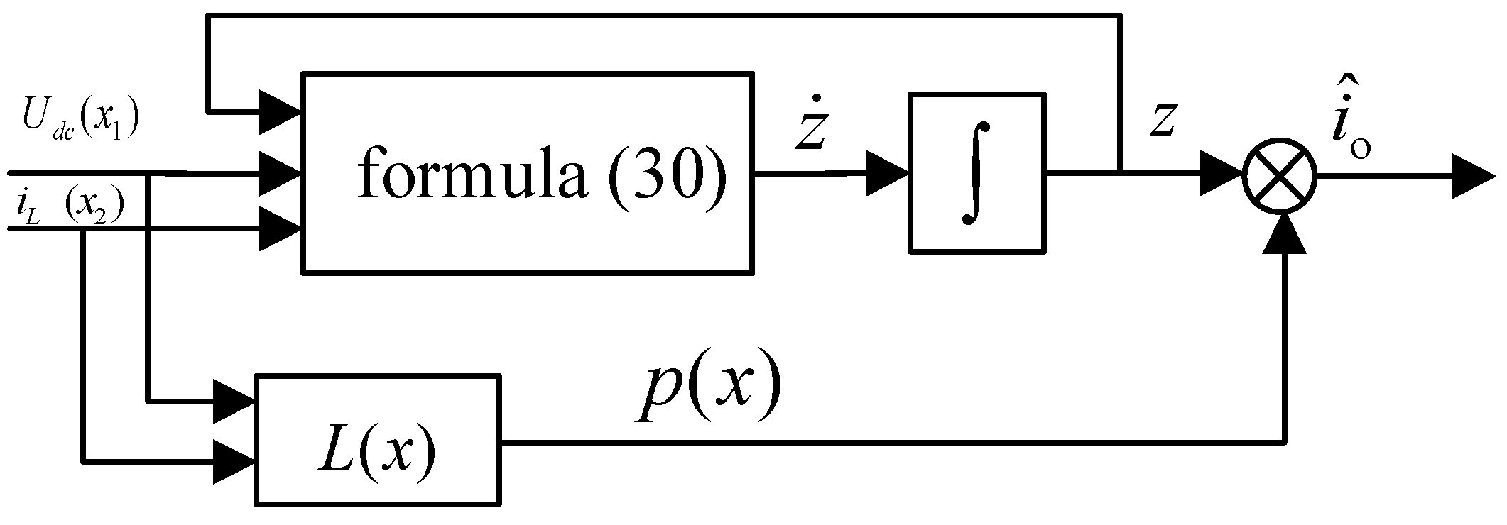
Substituting (26) (28) into (25), a nonlinear disturbance observer as shown in Equation (30) can be designed to estimate the disturbance variable:
{ z ˙ = ( L ( x ) g 2 ( x ) ) z L ( x ) ( g 2 ( x ) p ( x ) + f ( x ) + g 1 ( x ) u ) i ^ o = z + p ( x )   .
The internal structure diagram of NDO is shown in Figure 7.
We assume that e d = i o i ^ o represents the disturbance estimation error. The disturbance term i o has the characteristic of lim t i ˙ o = i o . The dynamic error equation is derived as follows:
e ˙ d = i ˙ o i ^ ˙ o = L ( x ) g 2 ( x ) i ^ o L ( x ) g 2 ( x ) i o = L ( x ) g 2 ( x ) e d .
The disturbance estimation error ed can be derived as follows:
e d = e L ( x ) g 2 ( x ) t = e l u C 1 t .
The NDO will be convergent if L ( x ) g 2 ( x ) > 0 (lu < 0) as shown in Formula (32). In order to simplify the observer design and eliminate the influence of control signal u on the estimated value, we make the observer gain lu < 0 and li = 0. Equations of the nonlinear disturbance observer in different work modes are derived on the basis of the above analysis:
{ i ^ o = z + l u U d c z ˙ = l u C 1 z + l u 2 C 1 U d c l u C 1 U b i L U d c .

4. Simulation Results

The simulation model of the photovoltaic energy storage system is built in the Matlab/Simulink. The system simulation model is made up of two parts, which are the main circuit and the control circuit. In the control circuit, two custom modules are built by MATLAB Function in Simulink Library, which are used as current prediction controller and nonlinear disturbance observer, respectively. The system simulation parameters are shown in Table 1. The parameters of the nonlinear disturbance observer are obtained by the previous analysis.

4.1. Dynamic Performance Verification with a Step Load

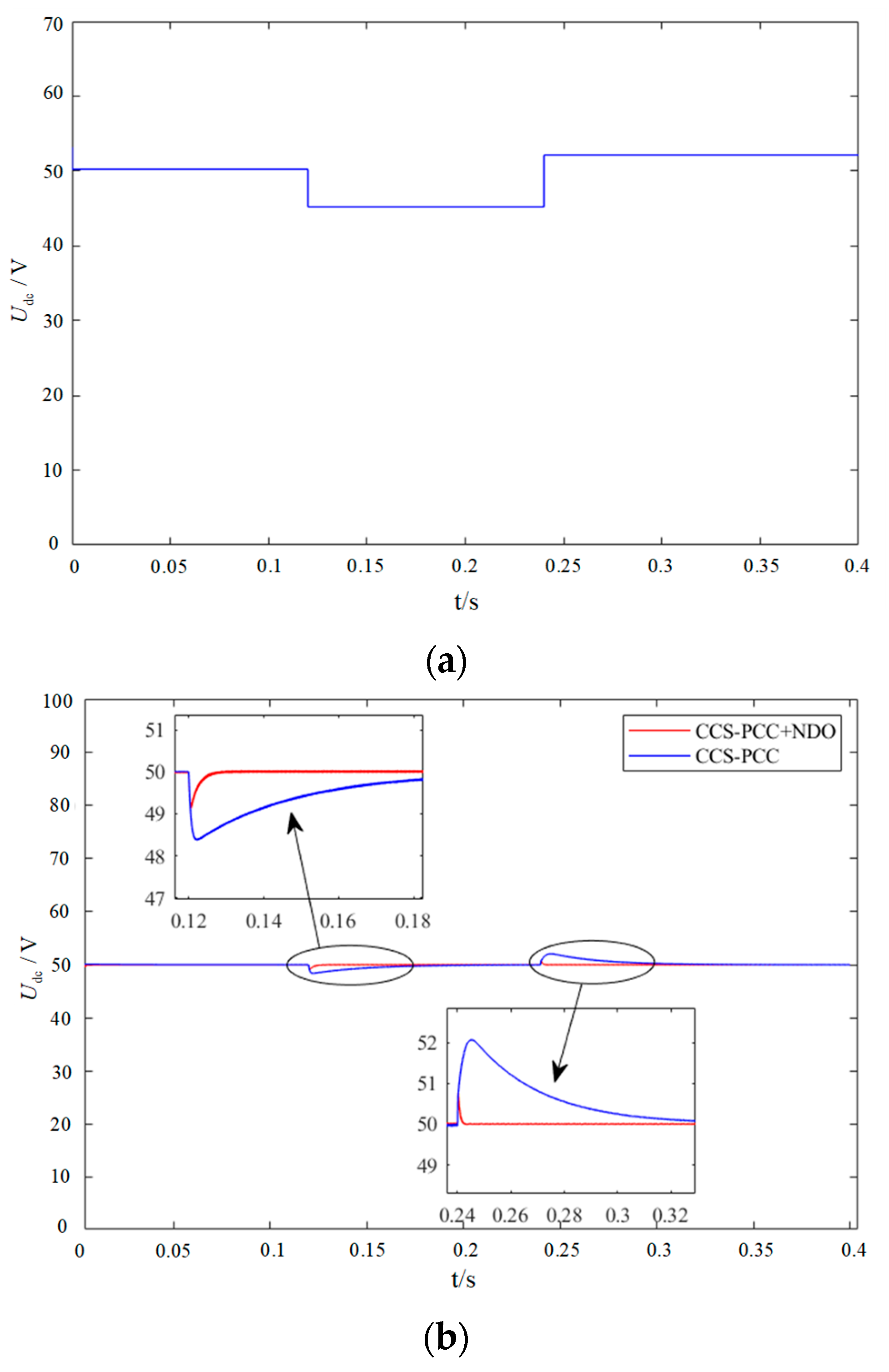
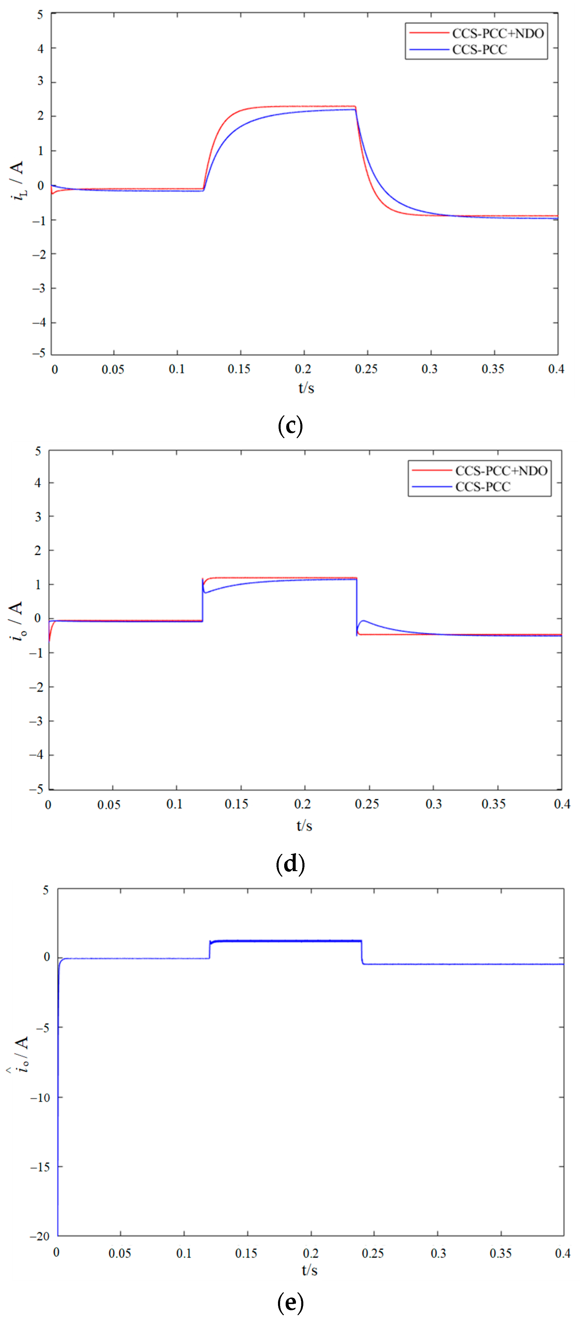
To verify the performance of the system with a step load, the comparative results between the CCS-PCC method and the proposed CCS-PCC+NDO method are shown in Figure 8. Figure 8a shows the DC bus voltage with a step load. The load steps up from 40 Ω to 20 Ω at 0.12 s suddenly, and the load steps down from 20 Ω to 60 Ω at 0.24 s. Figure 8b shows the controlled DC bus voltage by using CCS-PCC and CCS-PCC+NDO. Figure 8c,d show the inductor current and the equivalent load current, respectively. Figure 8e shows the observation value of the equivalent load current. These results show that the CCS-PCC+NDO method has better disturbance rejection capability and dynamic performance.

4.2. Dynamic Performance Verification with Photovoltaic Power Output Voltage Fluctuation

To verify the performance of the system with the PV output voltage fluctuation, the comparative results between the conventional CCS-PCC method and the proposed CCS-PCC+NDO method are given in Figure 9.
Figure 9a shows the fluctuated DC bus voltage. Figure 9b shows the controlled DC bus voltage by using CCS-PCC and CCS-PCC+NDO, respectively. Figure 9c shows the inductor current. Figure 9d shows the equivalent load current. Figure 9e shows the observation value of the equivalent load current from the NDO. These results show that the CCS-PCC+NDO method has better disturbance rejection capability and dynamic performance owing to good compensation in the process of PV output voltage fluctuation.

5. Experimental Results

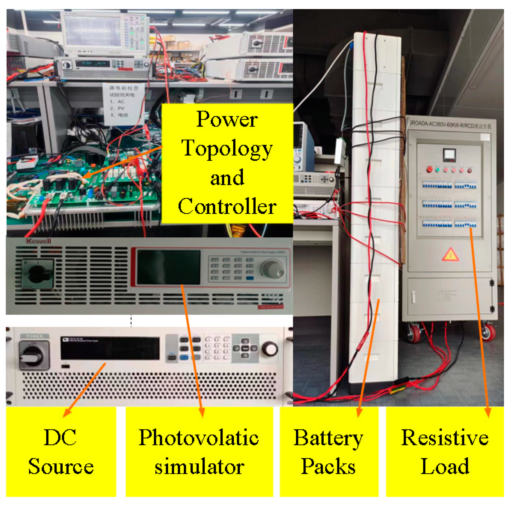
To verify the performance of the current predictive control method based on the nonlinear disturbance observer proposed in this paper in practical application, taking DSP28346 as the kernel, a photovoltaic energy storage system experimental platform with a bidirectional DC/DC converter was built. The experimental platform is shown in Figure 10. The system hardware consists of a DC source, batteries, a bidirectional DC/DC converter, resistive loads and an oscilloscope. The DC source is used to analog the output voltage of PV in different modes. The bidirectional DC/DC converter is the core of the system. Batteries can work in a charge state and a discharge state, and the batteries’ discharge current is positive in the experiment. The system experiment parameters are shown in Table 2.

5.1. Correctness Verification of CCS-PCC+NDO in Different Operation Modes

5.1.1. Boost Mode

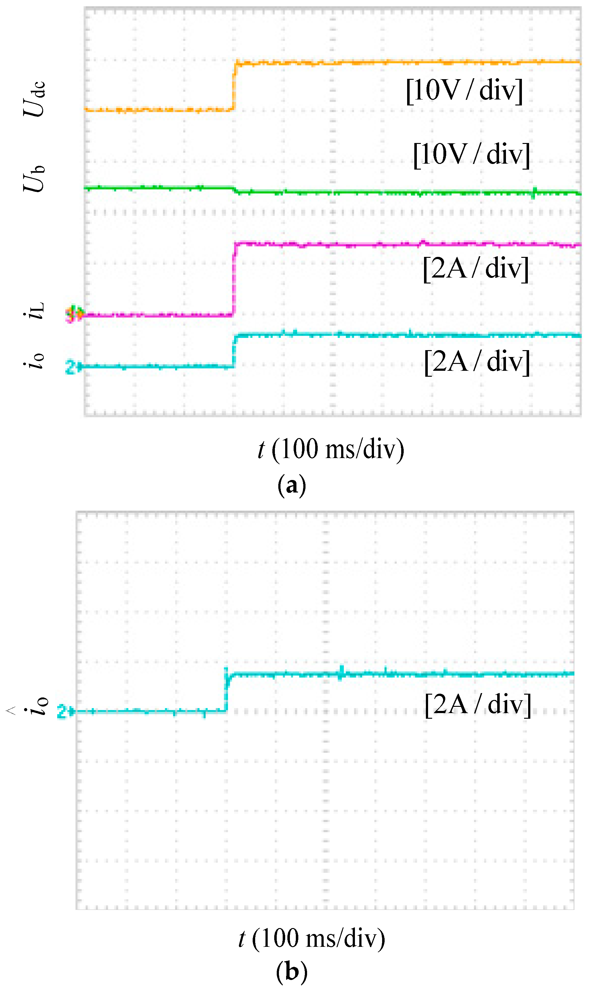
Using a DC source to analog PV output voltage up to 40 V, the reference value of the DC bus voltage is 50 V, the bidirectional DC/DC converter works in boost mode, and the batteries discharge to the loads. Figure 11 shows the system output waveforms in boost mode.
When the light intensity is lower or the temperature is higher, the PV output voltage after the maximum power is lower than the DC bus voltage reference value. It can be seen from Figure 11a that the DC bus voltage can be increased and the stability of the DC bus voltage can be ensured by the proposed control method. The batteries’ voltage is constant, basically, and the batteries work in the appropriate discharge state. The inductor current is positive. Figure 11b shows the observed value of the equivalent load current can track the actual current accurately.

5.1.2. Buck Mode

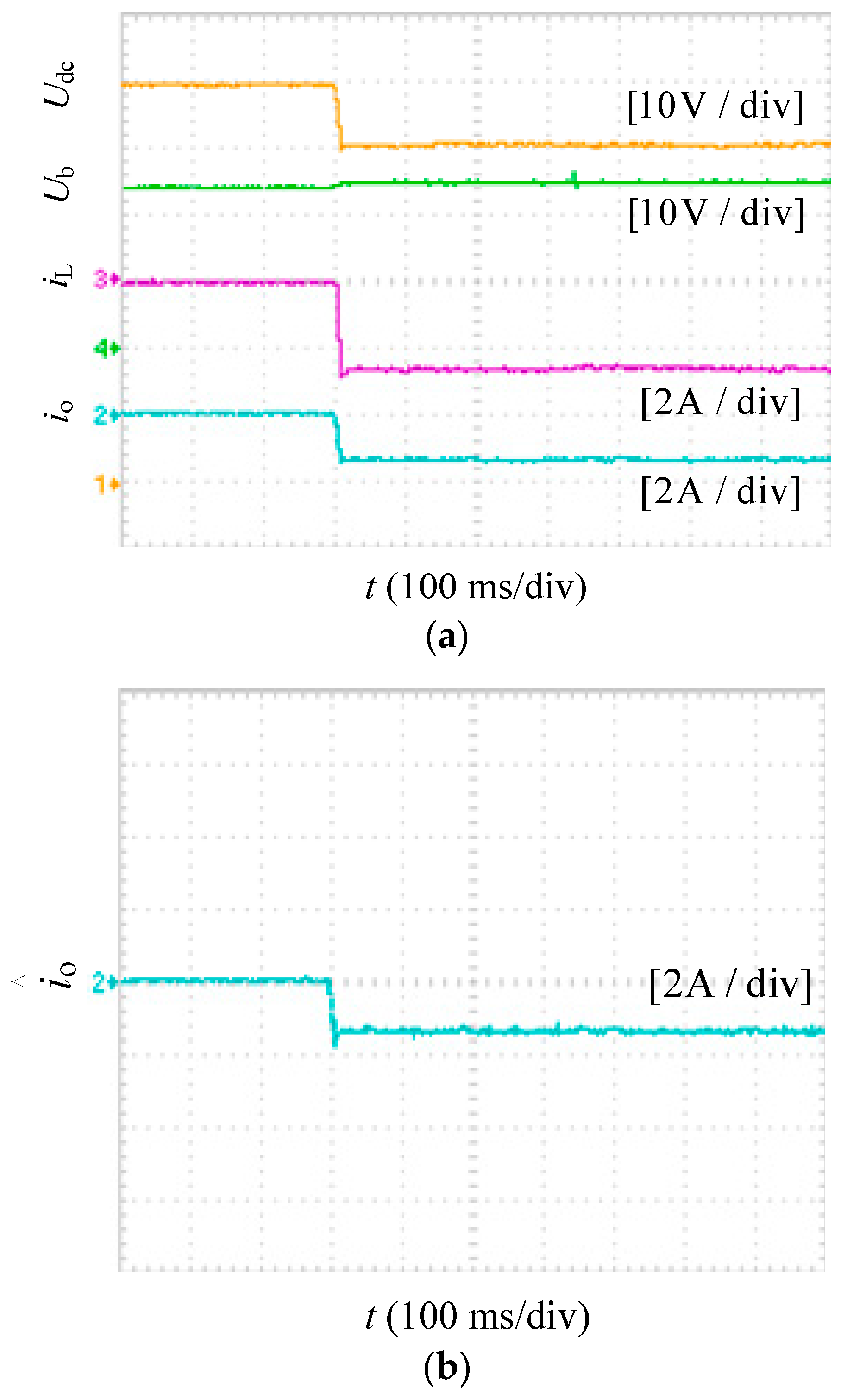
Using a DC source to analog PV output voltage up to 60 V, the reference value of the DC bus voltage is 50 V, the bidirectional DC/DC converter works in buck mode, and batteries are in the charge state. Figure 12 shows the system output waveforms in buck mode.
When the light intensity is higher or the temperature is lower, the PV output voltage after maximum power tracking is higher than the DC bus voltage reference value. It can be seen from Figure 12a that the DC bus voltage can be reduced and the stability of the DC bus voltage can be ensured by using CCS-PCC+NDO. The batteries’ voltage is constant, basically, and batteries work in the appropriate charge state. The inductor current is negative. Figure 12b shows the observed value of the equivalent load current can track the actual current accurately.

5.2. Dynamic Performance Verification with a Step Load

5.2.1. Boost Mode

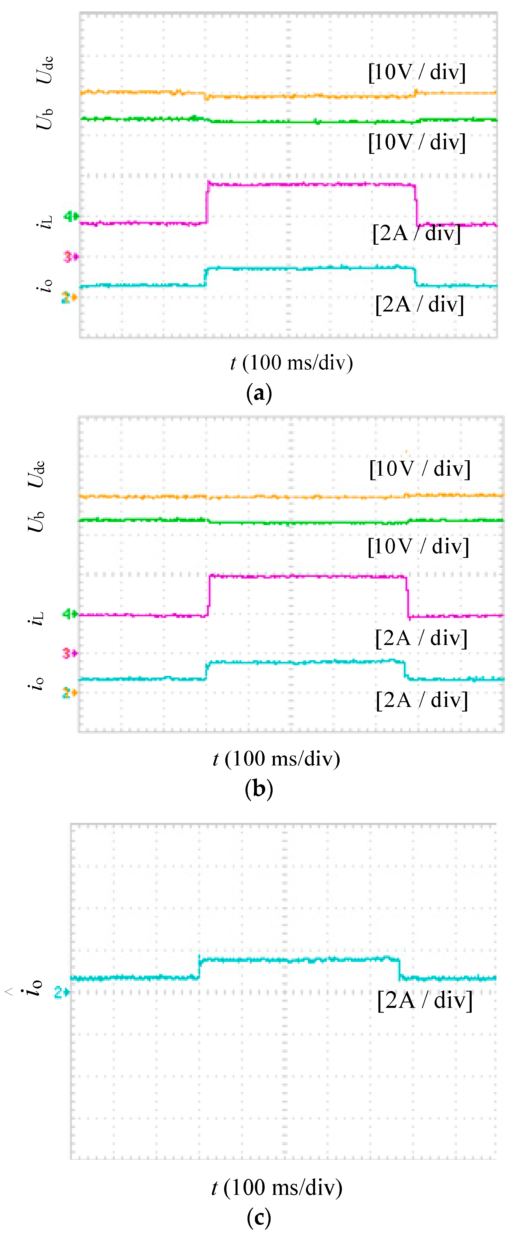
The bidirectional DC/DC converter works in boost mode under this condition, and the batteries work in the discharge state. The sudden load steps up from 40 Ω to 20 Ω, and then steps down from 20 Ω to 40 Ω. Figure 13 shows the system output waveforms by using CCS-PCC and CCS-PCC+NDO in boost mode.
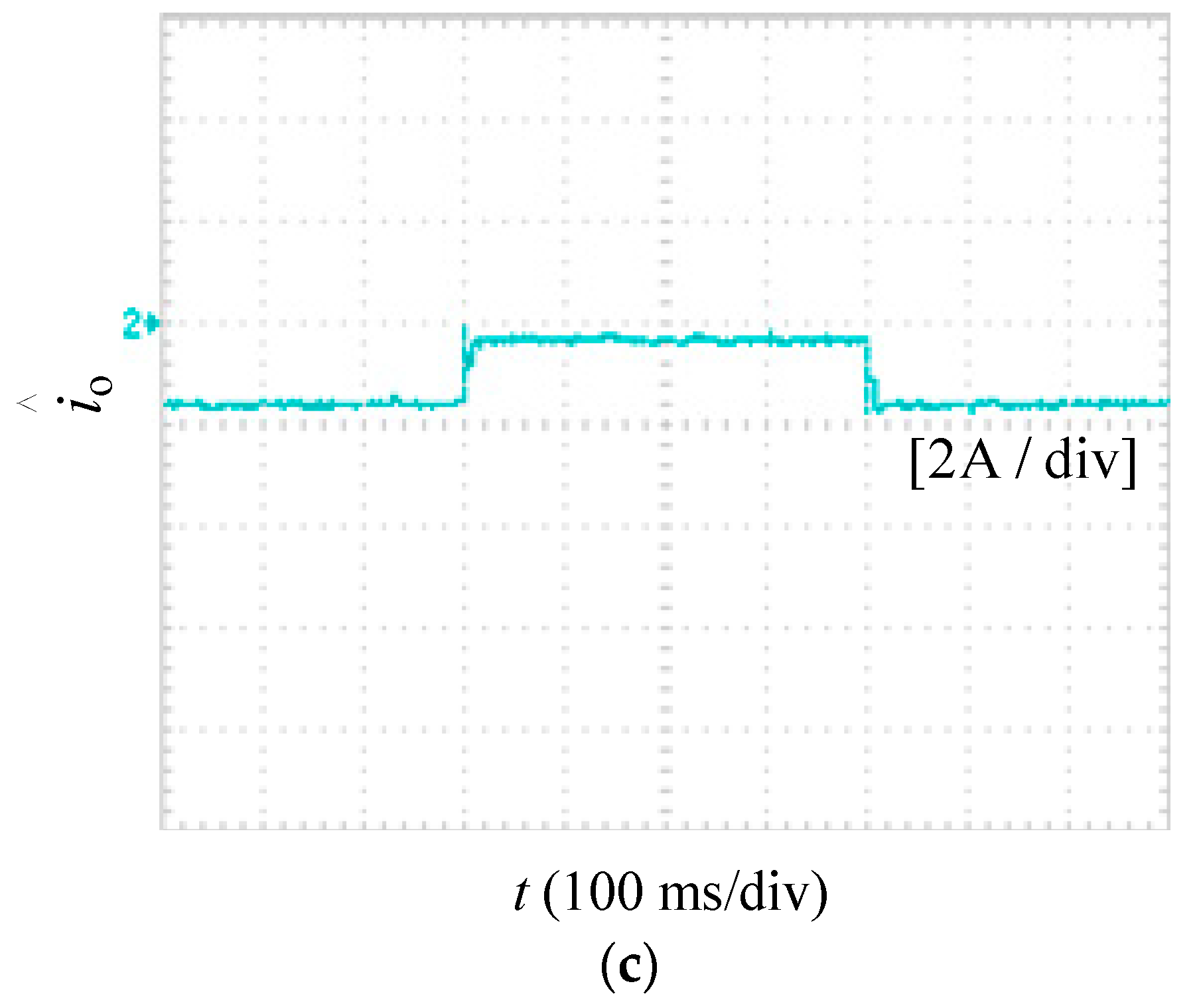
It can be seen from Figure 13a,b that the DC bus voltage can be maintained at 50 V, basically, with the step load under both control methods. When the system load steps up from 40 Ω to 20 Ω, the overshoot of the DC bus voltage is about 2.1 V, the settling time is 16 ms and the steady-state error of the DC bus voltage is 0.9 V with the CCS-PCC method. The overshoot of the DC bus voltage is about 1.6 V, the settling time is 14 ms and the steady-state error of DC bus voltage is 0.2 V with the CCS-PCC+NDO method. When the load steps down from 20 Ω to 40 Ω, the overshoot of the DC bus voltage is about 0.9 V, the settling time is 10 ms and the steady-state error of the DC bus voltage is 0.4 V with the CCS-PCC method. The overshoot of the DC bus voltage is about 0.8 V, the settling time is 9 ms and the steady-state error of the DC bus voltage is 0.3 V with the CCS-PCC+NDO method. Figure 13c shows the equivalent load current obtained from the NDO. Comparing Figure 13b,c, it can be seen that the observation value of the equivalent load current can track the actual current accurately. The DC bus voltage performance indexes in boost mode are presented in Table 3.

5.2.2. Buck Mode

Figure 14 shows the system output waveforms by using CCS-PCC and CCS-PCC+NDO in buck mode. The batteries work in the charge state when the bidirectional DC/DC converter works in buck mode. The sudden load steps up from 40 Ω to 20 Ω, and then steps down from 20 Ω to 40 Ω.
It can be seen from Figure 14a, b that the DC bus voltage can be maintained at 50 V, basically, with the step load under both control methods. When the system load steps up from 40 Ω to 20 Ω, the overshoot of the DC bus voltage is about 1.9 V, the settling time is 18 ms and the steady-state error of the DC bus voltage is 0.8 V with the CCS-PCC method. The overshoot of the DC bus voltage is about 1.6 V, the settling time is 10 ms and the steady-state error of the DC bus voltage is 0.5 V with the CCS-PCC+NDO method. When the load steps down from 20 Ω to 40 Ω, the overshoot of the DC bus voltage is about 2.2 V, the settling time is 12 ms and the steady-state error of the DC bus voltage is 0.7 V with the CCS-PCC method. The overshoot of the DC bus voltage is about 1.0 V, the settling time is 10 ms and the steady-state error of the DC bus voltage is 0.2 V with the CCS-PCC+NDO method. It can be seen that the observed value of the equivalent load current can track the actual current accurately from Figure 14c. The DC bus voltage performance indexes in buck mode are presented in Table 4.

5.2.3. Different Modes Switch

In this condition, the DC bus voltage is higher than the reference value when the load is 40 Ω, and the bidirectional DC/DC converter works in buck mode and the batteries are charged. When the load is switched from 40 Ω to 17 Ω, the DC bus voltage is lower than the reference value. The converter works in boost mode and the batteries are discharged. Figure 15 shows the system output waveforms.
It can be seen from Figure 15 that when the bidirectional DC/DC converter starts running the DC bus voltage can be maintained at 50 V, basically, during the load mutation process. The DC bus voltage performance indexes of the two control methods are shown in Table 5. It can be seen from Table 5 that the regulation time of the DC bus voltage is shorter and the overshoot of the DC bus voltage is smaller when using CSS-PCC+NDO than with CSS-PCC. The batteries work in the corresponding charge state and discharge state. It can be concluded from the above experimental results that the system with a step load has a more rapidly dynamic process and better robustness by using the CSS-PCC+NDO method in the experiment.

5.3. Performance Verification with Photovoltaic Power Output Voltage Fluctuation

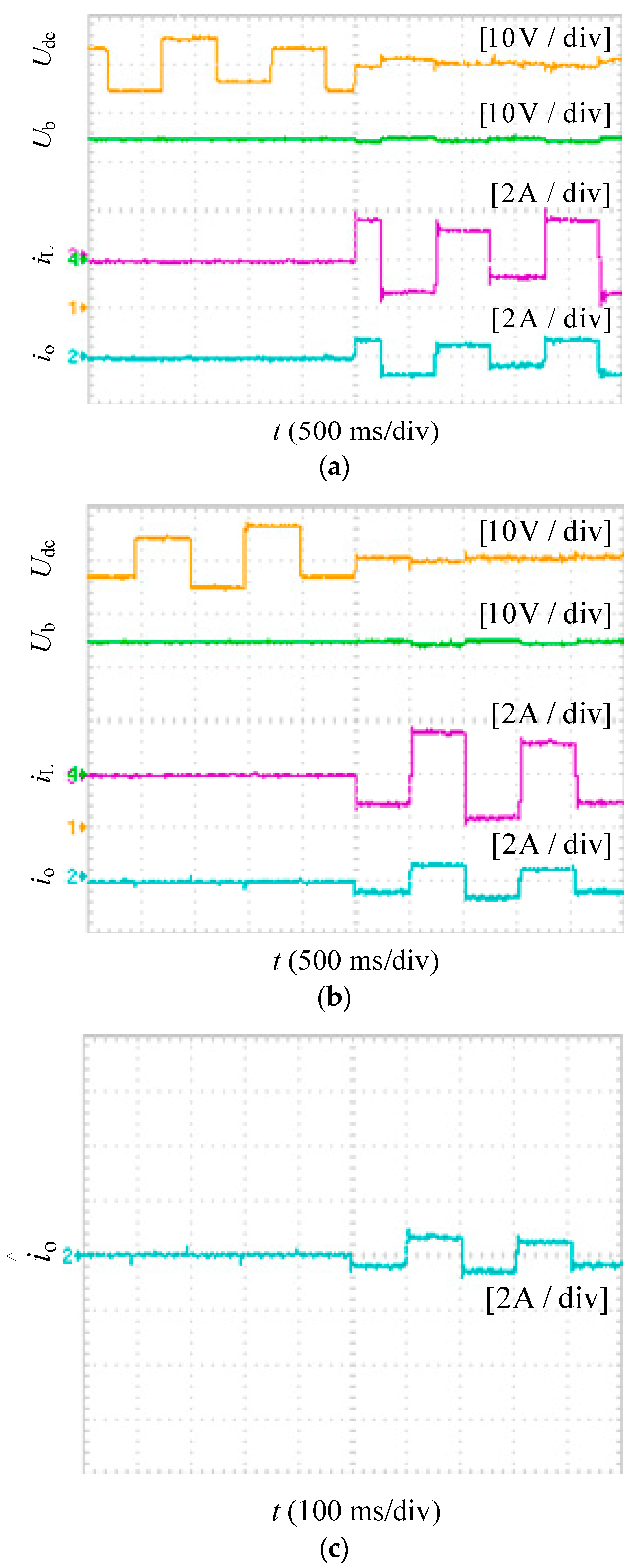
Using a DC source and a boost circuit to analog the fluctuating PV output voltage, which fluctuates between 40 V and 60 V, the system output waveforms are shown in Figure 16. It can be seen from the experimental results in Figure 16 that when the PV output voltage fluctuates greatly due to external influences the DC bus voltage can be ensured to be stable at 50 V, basically, by the control method proposed in this paper, the batteries work in the corresponding charge state and discharge state, and the inductor current ripple is small.

6. Conclusions

A robust continuous set control predictive current control based on a nonlinear disturbance observer was developed to address the problem of DC bus voltage fluctuation.
The fluctuation occurs due to the change in PV output power, load mutations and nonlinear load connection in the photovoltaic energy storage systems. The simulation and experimental results show that the disturbance rejection capability and the dynamic performance, in the case of a step load and PV output power fluctuation, can be effectively enhanced by the CCS-PCC+NDO method. However, the CCS-PCC method has strong dependence on the precise mathematical model of the controlled plant. In order to enhance the system’s robustness against perturbation and model mismatch, future studies will be performed to test the effectiveness of the data-driven MPC method.

Author Contributions

Conceptualization H.Y. and X.S.; methodology, H.Y.; software, H.L.; validation, H.L. and H.Y.; formal analysis, Q.Z.; investigation, H.L.; resources, Q.Z.; writing—original draft preparation, H.L.; writing—review and editing, H.Y.; supervision, X.S.; project administration, H.Y.; All authors have read and agreed to the published version of the manuscript.

Funding

This research was founded by the Doctoral Start-Up Foundation of Xi’an University of Technology. Grant number 119-451121001.

Conflicts of Interest

The authors declare no conflict of interest.

References

  1. Rana, M.M.; Uddin, M.; Sarkar, M.R.; Shafiullah, G.M.; Mo, H.; Atef, M. A review on hybrid photovoltaic–Battery energy storage system: Current status, challenges, and future directions. J. Energy Storage 2022, 51, 104597. [Google Scholar] [CrossRef]
  2. Wang, C.; Li, X.; Guo, L.; Li, Y.W. A Nonlinear-Disturbance-Observer-Based DC-Bus Voltage Control for a Hybrid AC/DC Microgrid. IEEE Trans. Power Electron. 2014, 29, 6162–6177. [Google Scholar] [CrossRef]
  3. Buticchi, G.; Costa, L.; Liserre, M. Improving System Efficiency for the More Electric Aircraft: A Look at DC/DC Converters for the Avionic Onboard DC Microgrid. IEEE Ind. Electron. Mag. 2017, 11, 26–36. [Google Scholar] [CrossRef]
  4. Subha, R.; Himavathi, S. Active power control of a photovoltaic system without energy storage using neural network-based estimator and modified P&O algorithm. IET Gener. Transm. Distrib. 2018, 12, 927–934. [Google Scholar]
  5. Hajebrahimi, H.; Kaviri, S.M.; Eren, S.; Bakhshai, A. A New Energy Management Control Method for Energy Storage Systems in Microgrids. IEEE Trans. Power Electron. 2020, 35, 11612–11624. [Google Scholar] [CrossRef]
  6. Gu, Y.; Xiang, X.; Li, W.; He, X. Mode-Adaptive Decentralized Control for Renewable DC Microgrid with Enhanced Reliability and Flexibility. IEEE Trans. Power Electron. 2014, 29, 5072–5080. [Google Scholar] [CrossRef]
  7. Prabhakaran, P.; Goyal, Y.; Agarwal, V. Novel Nonlinear Droop Control Techniques to Overcome the Load Sharing and Voltage Regulation Issues in DC Microgrid. IEEE Trans. Power Electron. 2018, 33, 4477–4487. [Google Scholar] [CrossRef]
  8. Xu, Q.; Vafamand, N.; Chen, L.; Dragicevic, T.; Xie, L.; Blaabjerg, F. Review on Advanced Control Technologies for Bidirectional DC/DC Converters in DC Microgrids. IEEE J. Emerg. Sel. Top. Power Electron. 2021, 9, 1205–1221. [Google Scholar] [CrossRef]
  9. Wu, Y.-E.; Ke, Y.-T. A Novel Bidirectional Isolated DC-DC Converter with High Voltage Gain and Wide Input Voltage. IEEE Trans. Power Electron. 2021, 36, 7973–7985. [Google Scholar] [CrossRef]
  10. Molavi, N.; Adib, E.; Farzanehfard, H. Soft-switching bidirectional DC–DC converter with high voltage conversion ratio. IET Power Electron. 2018, 11, 33–42. [Google Scholar] [CrossRef]
  11. Rezvanyvardom, M.; Mirzaei, A. Zero-Voltage Transition Nonisolated Bidirectional Buck–Boost DC–DC Converter with Coupled Inductors. IEEE J. Emerg. Sel. Top. Power Electron. 2021, 9, 3266–3275. [Google Scholar] [CrossRef]
  12. Santra, S.B.; Chatterjee, D.; Siwakoti, Y.P. Coupled Inductor Based Soft Switched High Gain Bidirectional DC-DC Converter with Reduced Input Current Ripple. IEEE Trans. Ind. Electron. 2023, 70, 1431–1443. [Google Scholar] [CrossRef]
  13. Mukherjee, N.; Strickland, D. Control of Cascaded DC–DC Converter-Based Hybrid Battery Energy Storage Systems—Part II: Lyapunov Approach. IEEE Trans. Ind. Electron. 2016, 63, 3050–3059. [Google Scholar] [CrossRef]
  14. Cornea, O.; Andreescu, G.-D.; Muntean, N.; Hulea, D. Bidirectional Power Flow Control in a DC Microgrid through a Switched-Capacitor Cell Hybrid DC–DC Converter. IEEE Trans. Ind. Electron. 2017, 64, 3012–3022. [Google Scholar] [CrossRef]
  15. Kumar, V.; Mohanty, S.R.; Kumar, S. Event Trigger Super Twisting Sliding Mode Control for DC Micro Grid with Matched/Unmatched Disturbance Observer. IEEE Trans. Smart Grid 2020, 11, 3837–3849. [Google Scholar] [CrossRef]
  16. Mosayebi, M.; Sadeghzadeh, S.M.; Gheisarnejad, M.; Khooban, M.H. Intelligent and Fast Model-Free Sliding Mode Control for Shipboard DC Microgrids. IEEE Trans. Transp. Electrif. 2021, 7, 1662–1671. [Google Scholar] [CrossRef]
  17. Hassan, M.A.; He, Y. Constant Power Load Stabilization in DC Microgrid Systems Using Passivity-Based Control with Nonlinear Disturbance Observer. IEEE Access 2020, 8, 92393–92406. [Google Scholar] [CrossRef]
  18. Melath, G.; Hussain, M.N.; Agarwal, V. A Nonlinear Adaptive Backstepping Controller for Stabilizing the DC Bus Voltage of an Islanded Hybrid Microgrid. IEEE J. Emerg. Sel. Top. Ind. Electron. 2022, 3, 538–548. [Google Scholar] [CrossRef]
  19. Wang, F.; Mei, X.; Rodriguez, J.; Kennel, R. Model predictive control for electrical drive systems—An overview. CES Trans. Electr. Mach. Syst. 2017, 1, 219–230. [Google Scholar] [CrossRef]
  20. Sun, C.; Sun, D.; Chen, W.; Nian, H. Improved Model Predictive Control with New Cost Function for Hybrid-Inverter Open-Winding PMSM System Based on Energy Storage Model. IEEE Trans. Power Electron. 2021, 36, 10705–10715. [Google Scholar] [CrossRef]
  21. Zhang, Z.; Wang, Z.; Wei, X.; Liang, Z.; Kennel, R.; Rodriguez, J. Space-Vector-Optimized Predictive Control for Dual Three-Phase PMSM with Quick Current Response. IEEE Trans. Power Electron. 2022, 37, 4453–4462. [Google Scholar] [CrossRef]
  22. Abu-Ali, M.; Berkel, F.; Manderla, M.; Reimann, S.; Kennel, R.; Abdelrahem, M. Deep Learning-Based Long-Horizon MPC: Robust, High Performing, and Computationally Efficient Control for PMSM Drives. IEEE Trans. Power Electron. 2022, 37, 12486–12501. [Google Scholar] [CrossRef]
  23. Bauersfeld, L.; Spannagl, L.; Ducard, G.J.J.; Onder, C.H. MPC Flight Control for a Tilt-Rotor VTOL Aircraft. IEEE Trans. Aerosp. Electron. Syst. 2021, 57, 2395–2409. [Google Scholar] [CrossRef]
  24. Baier, C.R.; Ramirez, R.O.; Marciel, E.I.; Hernandez, J.C.; Melin, P.E.; Espinosa, E.E. FCS-MPC without Steady-State Error Applied to a Grid-Connected Cascaded H-Bridge Multilevel Inverter. IEEE Trans. Power Electron. 2021, 36, 11785–11799. [Google Scholar] [CrossRef]
  25. Salem, A.; Abido, M.A.; Blaabjerg, F. Common-Mode Voltage Mitigation of Dual T-Type Inverter Drives Using Fast MPC Approach. IEEE Trans. Ind. Electron. 2022, 69, 7663–7674. [Google Scholar] [CrossRef]
  26. Bouaouaou, H.; Lalili, D.; Boudjerda, N. Model predictive control and ANN-based MPPT for a multi-level grid-connected photovoltaic inverter. Electr. Eng. 2022, 104, 1229–1246. [Google Scholar] [CrossRef]
  27. Wei, Q.; Wu, B.; Xu, D.; Zargari, N.R. Model Predictive Control of Capacitor Voltage Balancing for Cascaded Modular DC–DC Converters. IEEE Trans. Power Electron. 2017, 32, 752–761. [Google Scholar] [CrossRef]
  28. Vafamand, N.; Yousefizadeh, S.; Khooban, M.H.; Bendtsen, J.D.; Dragicevic, T. Adaptive TS Fuzzy-Based MPC for DC Microgrids with Dynamic CPLs: Nonlinear Power Observer Approach. IEEE Syst. J. 2019, 13, 3203–3210. [Google Scholar] [CrossRef]
  29. Yang, H.; Chao, K.; Sun, X.; Zhang, Q.; Ren, B.; Yang, M. Robust Predictive Current Control for Photovoltaic Energy Storage System Based on Second-order Tracking Differentiator. In Proceedings of the 14th IEEE Conference on Industrial Electronics and Applications (ICIEA), Xi’an, China, 19–21 June 2019; pp. 2065–2070. [Google Scholar]
  30. Aguirre, M.; Kouro, S.; Rojas, C.A.; Vazquez, S. Enhanced Switching Frequency Control in FCS-MPC for Power Converters. IEEE Trans. Ind. Electron. 2021, 68, 2470–2479. [Google Scholar] [CrossRef]
  31. Liu, C.; Xing, X.; Du, C.; Zhang, B.; Zhang, C.; Blaabjerg, F. An Improved Model Predictive Control Method Using Optimized Voltage Vectors for Vienna Rectifier with Fixed Switching Frequency. IEEE Trans. Power Electron. 2023, 38, 358–371. [Google Scholar] [CrossRef]
  32. Wang, D.; Shen, Z.J.; Yin, X.; Tang, S.; Liu, X.; Zhang, C.; Wang, J.; Rodriguez, J.; Norambuena, M. Model Predictive Control Using Artificial Neural Network for Power Converters. IEEE Trans. Ind. Electron. 2022, 69, 3689–3699. [Google Scholar] [CrossRef]
  33. Guler, N.; Biricik, S.; Bayhan, S.; Komurcugil, H. Model Predictive Control of DC–DC SEPIC Converters with Autotuning Weighting Factor. IEEE Trans. Ind. Electron. 2021, 68, 9433–9443. [Google Scholar] [CrossRef]
  34. Zhang, X.; Wang, B.; Gamage, D.; Ukil, A. Model Predictive Control Based Dynamic Power Loss Prediction for Hybrid Energy Storage System in DC Microgrids. IEEE Trans. Ind. Electron. 2022, 69, 8080–8090. [Google Scholar] [CrossRef]
  35. Liu, X.; Qiu, L.; Wu, W.; Ma, J.; Fang, Y.; Peng, Z.; Wang, D.; Rodriguez, J. Event-Triggered ESO-Based Robust MPC for Power Converters. IEEE Trans. Ind. Electron. 2023, 70, 2144–2152. [Google Scholar] [CrossRef]
  36. Bao, Y.; Wang, L.Y.; Wang, C.; Jiang, J.; Jiang, C.; Duan, C. Adaptive Feedforward Compensation for Voltage Source Disturbance Rejection in DC–DC Converters. IEEE Trans. Control Syst. Technol. 2018, 26, 344–351. [Google Scholar] [CrossRef]
  37. Yang, J.; Zheng, W.X.; Li, S.; Wu, B.; Cheng, M. Design of a Prediction-Accuracy-Enhanced Continuous-Time MPC for Disturbed Systems via a Disturbance Observer. IEEE Trans. Ind. Electron. 2015, 62, 5807–5816. [Google Scholar] [CrossRef]
  38. Lin, X.; Guo, L.; Feng, Y.; Wang, C.; Lin, M. A Nonlinear Disturbance Observer Based DC Bus Voltage Control for a DC microgrid. Proc. CSEE 2016, 36, 350–359. [Google Scholar]
  39. Li, S.; Yang, J. Robust Autopilot Design for Bank-to-Turn Missiles using Disturbance Observers. IEEE Trans. Aerosp. Electron. Syst. 2013, 49, 558–579. [Google Scholar] [CrossRef]
Figure 1. The structure of a typical islanded DC microgrid.
Electronics 12 01985 g001
Figure 2. The operational principle of the bidirectional DC/DC converter. (a) Boost mode. (b) Buck mode.
Electronics 12 01985 g002
Figure 3. The system control structure diagram.
Electronics 12 01985 g003
Figure 4. Block diagram of CCS-PCC controller.
Electronics 12 01985 g004
Figure 5. Control block diagram of the usual DC bus voltage.
Electronics 12 01985 g005
Figure 6. Control block diagram of the NDO-feedforward-based DC bus voltage.
Electronics 12 01985 g006
Figure 7. Internal structure diagram of the NDO.
Electronics 12 01985 g007
Figure 8. The comparative results of the system with a step load. (a) The DC bus voltage. (b) The controlled DC bus voltage. (c) The inductor current. (d) The equivalent load currents. (e) The output of the NDO.
Electronics 12 01985 g008aElectronics 12 01985 g008b
Figure 9. The comparative results of the system in the case of DC bus voltage fluctuation. (a) The fluctuated DC bus voltage. (b) The controlled DC bus voltage. (c) The inductor current. (d) The equivalent load currents. (e) The output of the NDO.
Electronics 12 01985 g009aElectronics 12 01985 g009b
Figure 10. Experimental platform.
Electronics 12 01985 g010
Figure 11. System output waveforms in boost mode. (a) The waves of U d c , U b , i L , i o . (b) The output of NDO.
Electronics 12 01985 g011
Figure 12. System output waveforms in buck mode. (a) The waves of U d c , U b , i L , and i o . (b) The output of NDO.
Electronics 12 01985 g012
Figure 13. System output waveforms with a step load in boost mode. (a) CCS-PCC. (b) CCS-PCC+NDO. (c) The output of NDO.
Electronics 12 01985 g013
Figure 14. System output waveforms with a step load in buck mode. (a) CCS-PCC. (b) CCS-PCC+NDO. (c) The output of NDO.
Electronics 12 01985 g014aElectronics 12 01985 g014b
Figure 15. System output waveforms with a step load in the different modes switch. (a) CCS-PCC. (b) CCS-PCC+NDO. (c) The output of NDO.
Electronics 12 01985 g015
Figure 16. System output waveforms in the case of DC bus voltage fluctuation. (a) CCS-PCC. (b) CCS-PCC+NDO. (c) The output of NDO.
Electronics 12 01985 g016
Table 1. System simulation parameters.
Simulation ParametersValue
Given DC bus voltage (V)50
Batteries’ terminal voltage (V)24
Inductor (mH)2.5
Capacitor of DC bus (μF)470
DC load (Ω)40
Observer gain ( l u )−0.75
Sampling frequency (kHz)20
Table 2. System experiment parameters.
Experiment ParametersValue
Given DC bus voltage (V)50
Batteries’ terminal voltage (V)24
Capacitor of DC bus (μF)470
Inductor (mH)2.5
DC load (Ω)40
Sampling frequency (kHz)20
Table 3. The DC bus voltage performance indexes comparison in boost mode.
Load40 Ω → 20 Ω20 Ω → 40 Ω
Control StrategyCCS-PCCCCS-PCC+NDOCCS-PCCCCS-PCC+NDO
Overshoot4.2% (2.1 V)3.2% (1.6 V)1.8% (0.9 V)1.6% (0.8 V)
Settling time0.016 s0.014 s0.010 s0.009 s
Steady-state error0.9 V0.2 V0.4 V0.3 V
Table 4. The DC bus voltage performance indexes comparison in Buck mode.
Load40 Ω → 20 Ω20 Ω → 40 Ω
Control StrategyCSS-PCCCSS-PCC+NDOCSS-PCCCSS-PCC+NDO
Overshoot3.8% (1.9 V)3.2% (1.6 V)4.4% (2.2 V)2% (1 V)
Settling time0.018 s0.010 s0.012 s0.010 s
Steady-state error0.8 V0.5 V0.7 V0.2 V
Table 5. The DC bus voltage performance indexes in different modes switch.
Load40 Ω → 17 Ω
Control StrategyCSS-PCCCSS-PCC+NDO
Overshoot4.6% (2.3 V)1.6% (0.8 V)
Settling time0.016 s0.008 s
Steady-state error1.1 V0.3 V
Disclaimer/Publisher’s Note: The statements, opinions and data contained in all publications are solely those of the individual author(s) and contributor(s) and not of MDPI and/or the editor(s). MDPI and/or the editor(s) disclaim responsibility for any injury to people or property resulting from any ideas, methods, instructions or products referred to in the content.