1. Introduction
Monolithic battery power and self-powered energy harvesting are two major research hotspots amongst the current methods of powering portable products. Monolithic battery power supply is an effective measure to achieve miniaturization and low power consumption of portable devices [
1,
2]. A typical single-cell NiMH battery has an open-circuit voltage of 1.2 V and a discharge voltage of about 0.8 V. Fuel cells have an open-circuit voltage of 0.8–0.9 V and a rated operating voltage of 0.6–0.8 V. Energy harvesting (EH) technologies collect energy from the surrounding environment, such as vibrational energy [
3,
4], thermal energy [
5,
6], solar energy [
7,
8], RF energy [
9,
10], and so on. These energies are then stored and boosted using interface circuits, so that they can be converted into a supply voltage for IoT-distributed devices, portable devices, and some other equipment. These are used to solve the problem of difficulty in replacing the batteries [
11,
12] or to extend the battery life [
13,
14]. The energy density of the ambient energy is weak [
15,
16], and the direct output voltage of the energy harvesting device is smaller. For example, the output voltage of a single solar cell is 0.4–0.7 V, while the operating voltage of hybrid circuits is typically 3.3 V and above. Therefore, a boost circuit is required to achieve voltage boosting when the power supply voltage used is smaller; for example, when a single-cell power supply or energy harvesting power supply is used [
17,
18].
Asynchronous boost converters and synchronous boost converters are two common types of boost converters. Different from asynchronous boost converters, higher efficiency can be achieved by using power switches instead of diodes in synchronous boost converters. Because of their flexible control modes and high conversion efficiency, synchronous boost converters are a preferred choice for powering portable products, sensor nodes and wearable, implantable devices. Conventional MOSFET devices have a threshold voltage near 0.75 V, so the boost converter needs to have the ability to self-start at near-threshold or even sub-threshold voltages when powered by a single battery or self-powered by energy harvesting. At the same time, in order to extend the service life of a single cell or to improve the energy utilization efficiency of the energy harvesting booster unit, the conversion efficiency of the booster converter needs to be improved as much as possible. Especially when the input voltage is relatively low, the start-up process of the booster converter needs to minimize the losses caused by switching and other dissipation, otherwise it will not only reduce the efficiency of the booster converter, but even cause start-up failure.
Several boost converters that can be started at several hundred millivolts or even tens of millivolts have been proposed in the existing work. Some of these boost converters use complex auxiliary start-up circuits [
19], some resort to additional external devices [
20,
21], some have long start-up times [
22], and some use special semiconductor processes, such as low-voltage processes [
23] or negative-voltage processes [
24], which undoubtedly increase the production cost of chip fabrication. Moreover, to improve the efficiency of boost converters, some dual-mode [
25] or multi-mode [
26,
27] hybrid modulated boost converters have been proposed in recent years. However, these techniques are proposed to improve the efficiency of the boost converter during stable operation. The complex mode control unit during start-up at low input voltages will generate large losses and reduce the efficiency of the boost converter. Secondly, the switching of converter mode mainly relies on the voltage or current detection unit, and the operating state of the detection unit is not stable during the start-up process of low supply voltage. It is easy to cause confusion in the control logic of the boost converter, so the design space is provided for improving the efficiency of the boost converter on the basis of multi-mode control.
Staged starting is an effective method to achieve near-threshold starting [
28,
29,
30], where Ref. [
28] used a combination of initial, open-loop, and closed-loop states to start at an input voltage of 1 V. Ref. [
29] used a combination of staged starts and soft starts to achieve a start at an input voltage of 0.9 V. However, the boost converter only operates in PWM mode, which limits the efficiency of the converter at light loads. Ref. [
30] added an auxiliary power PMOS to the staged start to further reduce the converter start-up voltage, but increased the complexity of the control circuit. On the basis of ensuring that the boost converter can achieve a near-threshold start-up, there are several studies that propose some methods to further improve the converter efficiency or extend the battery life [
31,
32,
33]. In Ref. [
31], the incorporation of the Adaptive Sleeping Time Control (ASTC) technique improvds the power conversion efficiency of the converter at light loads. Ref. [
32] incorporated adaptive on-time (AOT) control techniques to improve the efficiency of the boost converter at light and heavy loads. Ref. [
33] used battery power and energy storage self-powered to extend the battery life, but incorporated more comparison and control modules that limit the minimum input voltage of the converter and the efficiency of the converter.
This paper presents an efficient synchronous boost converter with a near-threshold self-start function. The boost converter adopts a staged start-up approach and is capable of self-starting at near-threshold input voltages using a conventional semiconductor manufacturing process (threshold voltage of about 0.74 V) without introducing an auxiliary start-up unit or additional external components. No complex logic control unit is incorporated throughout the start-up process, and there is no voltage or current overshoot. Based on the multi-mode mixed modulation, the converter can achieve a smooth transition from soft-start to multi-mode mixed modulation mode, avoiding logic confusion during the start-up process and further improving the conversion efficiency of the boost converter.
This paper is organized as follows. The structure of the proposed boost converter and its mode of operation will be described in
Section 2, the circuit implementation will be analyzed in
Section 3, and the experimental results and conclusions will be discussed in
Section 4 and
Section 5.
2. The Structure of the Proposed Boost Converter and Its Mode of Operation
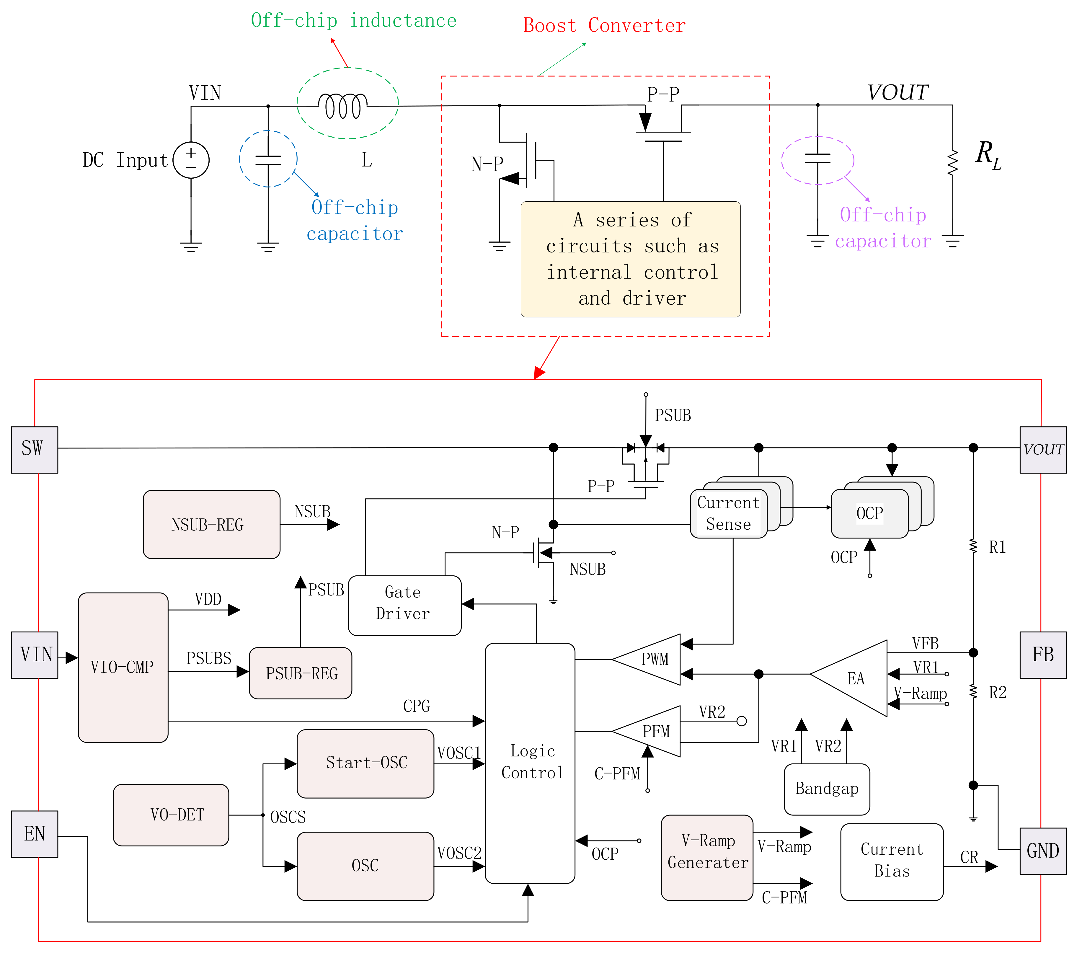
The structure of the proposed boost converter is shown in
Figure 1. When the boost converter operates in CCM (continuous current mode), the relationship between the output voltage
and the input voltage
can be expressed as
, where
D is the duty cycle of the converter. When the boost converter operates in CDM (discontinuous current mode), the relationship between the output voltage
and the input voltage
can be expressed as
,
is the ratio of the on-time of N-P to the oscillation period,
is the load resistance of the converter,
L is the inductance value of the off-chip inductor. The VIO-CMP module compares the input voltage
with the output voltage
of the boost converter and selects the larger of
or
as the supply voltage
of the boost converter. At the same time, when
is less than
, the power MOS P-P can be controlled to always be off, relying only on the conduction of the parasitic diode in the P-P to conduct the current to increase the output voltage
, reducing the power loss during the start-up process.
VO-DET is used to detect the output voltage and generate OSCS to select the oscillation signal, which controls the conduction of the Start-OSC oscillator when the output voltage is below the set target value (1.6 V) or before the reference voltage reaches the stable output (1.1 V). The Start-OSC oscillator generates a stable oscillation signal VOSC1 (VOSC1 controls the conduction of the N-P power MOS) as the oscillation signal for the boost converter when the input voltage is below the threshold voltage of the MOS device.
When the output voltage reaches the set target value (1.6 V) and the reference voltage generated by the internal bandgap (Bandgap) reaches a stable value (1.1 V), the OSCS signal is flipped so that the OSC oscillator (the output VOSC2 of the OSC oscillator is more stable than the output VOSC1 of the Start-OSC oscillator), the ramp voltage generation circuit V-Ramp-G (to generate the ramp voltage V-Ramp required for soft start), error amplifier EA, and PWM comparator start to conduct. VOSC2 controls the conduction of the N-P power MOS, after which the output signal of the Current Sense module and the output signal of the error amplifier EA are compared by the PWM module to generate the off signal to control the N-P.
The NSUB-REG module is capable of generating the NSUB regulation voltage according to the magnitude of the supply voltage, increasing the substrate voltage of N-P when the input voltage is low, reducing the threshold voltage using the bulk effect of MOS devices, and assisting the conduction of N-P under low voltage input conditions. The substrate voltage of N-P is automatically switched to low (ground voltage) when the supply voltage reaches the target value, and the whole regulation and switching process is performed without any comparator addition.
The V-Ramp-G module is not only able to generate the ramp voltage V-Ramp required for a soft start, but can also generate a C-PFM signal at the end of the soft start to control the PFM module to enter the normal working state, so that the startup of the boost converter is completed. After this, the boost converter will carry out PWM-PFM hybrid modulation according to the size of the load current. The boost converter maintains the PWM control mode during the soft start, reducing the risk of logic confusion during the start-up process.
Figure 2 shows the ideal process diagram for the start-up of the proposed boost converter.
Figure 2a shows a diagram of the start-up process when the input voltage of the boost converter
(threshold voltage of the power MOS), and the output voltage of the boost converter is roughly divided into five stages (1)–(5) at start-up. In phases (1)(2)(3), the output voltage does not reach 1.6 V (
), the oscillation signal of the boost converter is VOSC1, and the modules OSC, V-Ramp-G, EA, PWM, and PFM are turned off. In phases (1) and (2), the N-P power MOS is on and the P-P power MOS is off, relying on the conduction of the P-P’s parasitic diode to charge the off-chip capacitor. In phase (1), the parasitic diode cannot conduct due to the low input voltage, and at this time the off-chip inductor charges the parasitic junction capacitor of P-P, making the voltage at SW rise. This makes the parasitic diode conduct in phase (2) cause the output voltage VOUT to rise. In phase (3), the P-P power MOS conduction rises with a larger source-drain current compared to the parasitic diode conduction current and increased slope of the output voltage. The oscillation signal of the boost converter in phase (4) is VOSC2, the module Start-OSC is switched off, the module OSC, V-Ramp-G, EA, PWM is on, and the boost converter officially enters the soft-start phase. Phase (5) soft-start is finished, the PFM module turns on, and the boost converter officially enters the PWM-PFM hybrid modulation mode according to the load size.
Figure 2b shows a diagram of the ideal start-up process for a boost converter with input voltage
. Unlike
Figure 2a,
Figure 2b is divided into three main stages (1)(2)(3), where stages (2)(3) are the same as stages (4)(5) in
Figure 2a, respectively. In
Figure 2b, since
is relatively large, the parasitic diode in P-P can be turned on without charging the parasitic capacitor of P-P. Therefore, the output voltage VOUT starts to increase at the initial stage of power-up, and the on-current of the parasitic diode is less different from the source-leakage current when P-P is on, which is expressed in the output voltage waveform as a negligible change in the slope of the output voltage. The stages (1)(2)(3) in
Figure 2a are simplified to stage (1) in
Figure 2b.
3. Circuit Implementation
3.1. VIO-CMP
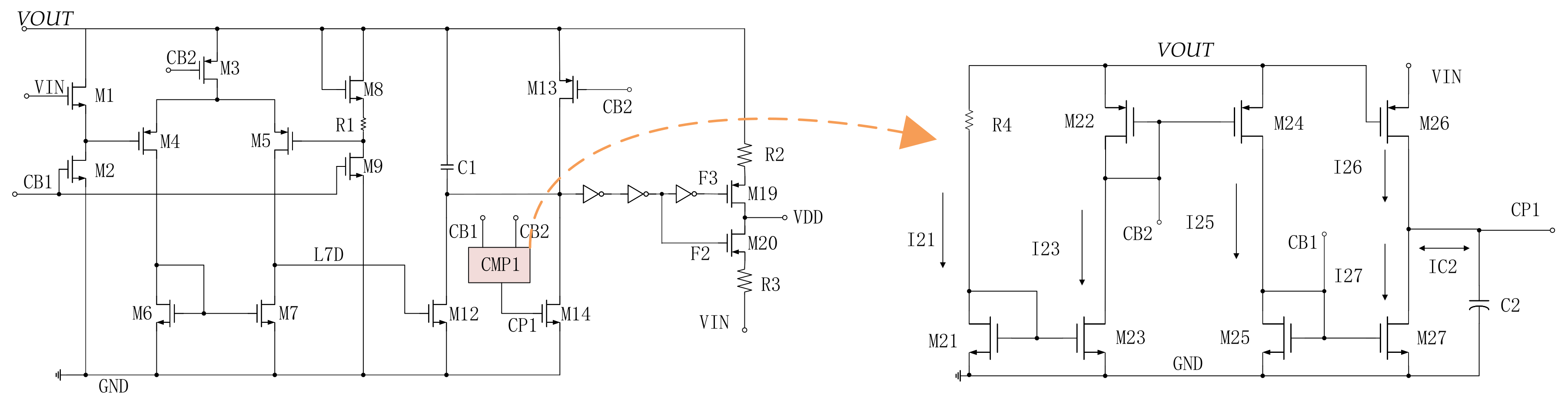
Figure 3 shows the circuit structure of the VIO-CMP module. A differential comparator operating in the saturation region has the advantages of high comparison accuracy and high PSRR. However, the comparator cannot operate in the saturation region when the supply voltage is relatively low, so appropriate low-voltage comparison measures are required when the supply voltage is relatively low.
When and , it will make , current charges the capacitor C2, and after a period of time, the voltage , so that F2 is low and F3 is high. This makes M20 turn on and M19 off, , where is the supply voltage of the boost converter. When and , the charging current of C2 is , and CP1 stays high; therefore, . When and , the charging current of C2 is , which makes C2 remain in the discharging state. After a period of time, CP1 becomes low, which in turn makes F2 high and F3 low. At this time, , adjusting the and can change the discharge rate of C2. When , the two-stage differential comparator consisting of M3-M11 has the condition of saturation conduction. This differential comparator can be used to compare the magnitude of and to determine the value of .
3.2. VO-DET
Figure 4 shows the circuit structure of the proposed VO-DET module. The main structure of this module is a differential comparator composed of M34-M38 in (3), which compares VFB1 (one of the feedback signals of the output voltage) with the reference voltage signal VR1 to obtain the OSCS signal to realize the selection of the control oscillation signal. However, this differential comparator does not work properly when the supply voltage is low and VR1 is a low unstable output. Therefore, the (1) and (2) structure is added to the VO-DET module to ensure that it can generate the correct OSCS signal under this condition. Confusion in the selection of the oscillation signal may cause the boost converter to fail to start normally. It is necessary to ensure that the VO-DET module has a certain anti-interference capability, so the Schmitt trigger structure is selected for INV1 in (1). It is used to reduce the adverse effects of the interference signals carried in
and
on the OSCS signal.
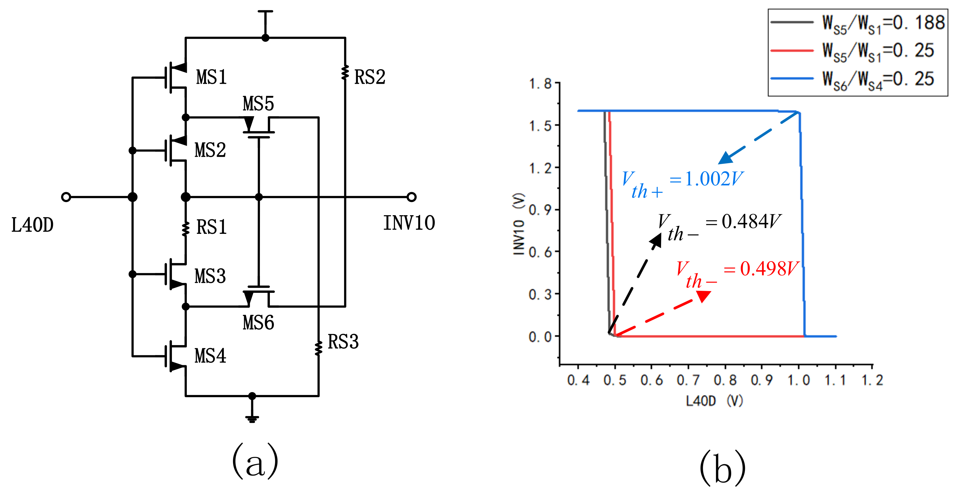
The circuit structure of INV1 is shown in
Figure 5a. The threshold voltages for the upper and lower turning points are
and
, respectively. The output signal INV1O of INV1 cannot be flipped from low to high when
. The flip thresholds of
and
are shown in Equation (
1), where
and
are the threshold voltages of the selected NMOS and PMOS, respectively.
is the aspect ratio of the MOS device with serial number
x. From Equation (
1), it can be seen that changing the size of
and
can achieve the purpose of adjusting
and
. In the power supply voltage of 1.6 V when the proposed order
,
,
,
, the calculation can be obtained
,
. Simulation of INV1 was performed according to this calculated value, and the simulation results obtained are shown in
Figure 5b. It can be seen that
,
at this time.
, when the
. In the design of INV1, the final choice is
,
.
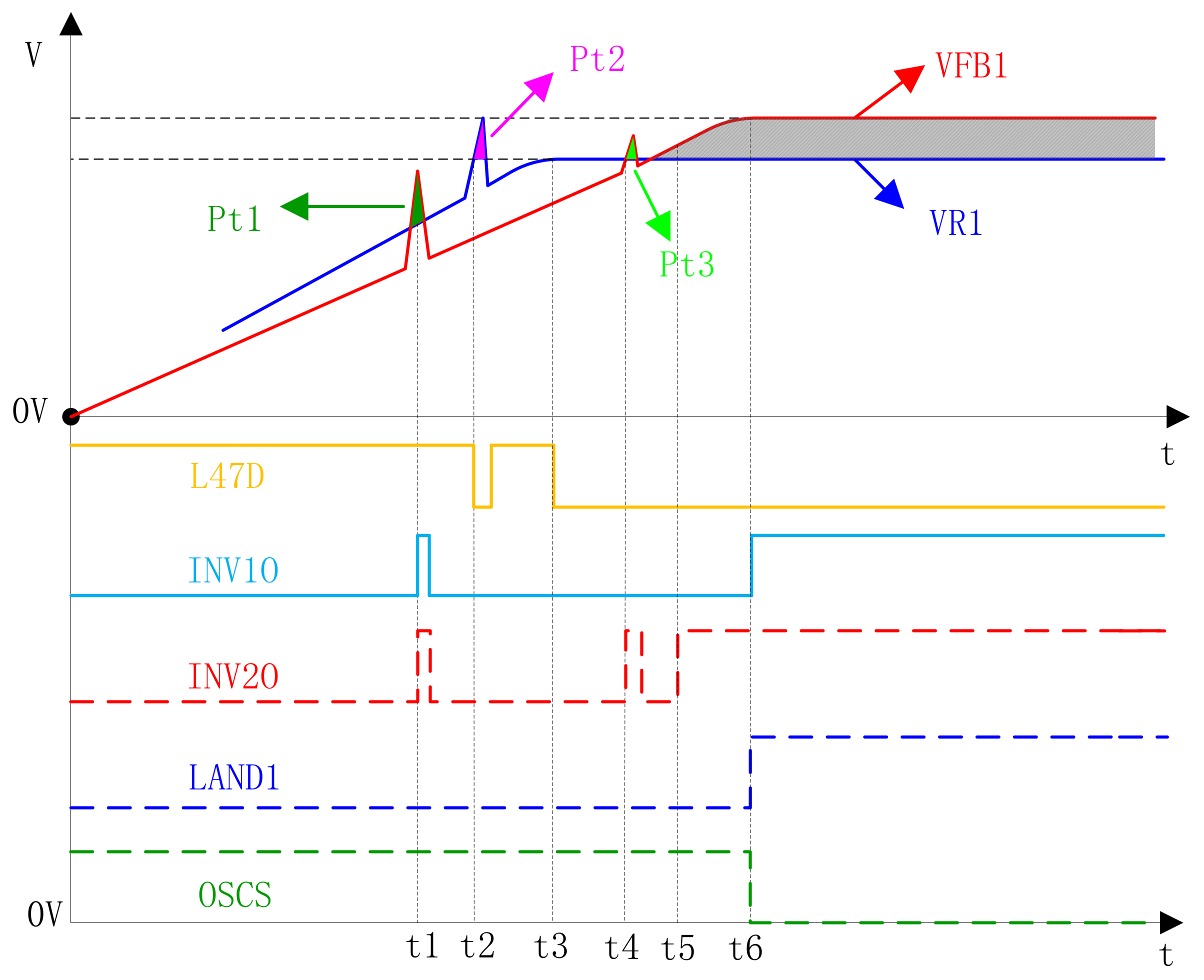
Figure 6 shows the logic diagram of the OSCS signal generated by the VO-DET. L47D remains high until
reaches a stable output of 1.1 V, INV2O flips to high when
, INV1O flips high when VFB1 > VR1 and output of the differential comparator
, otherwise INV1O stays low. When simultaneously ensuring that L47D is low and INV1O and INV2O are high, this means that the OSCS level flips to low only when VR1 reaches a stable output of 1.1 V,
and the output of the differential comparator
; otherwise it stays high (oscillating signal generated by Start-OSC).
At the moment of has a large burr spike making , and the output of the differential comparator , so INV1O and INV2O are flipped to a high level. However, at this time, VR1 has not reached 1.1V, L47D will remain high, and cannot meet the condition that L47D is and INV1O, INV2O are at the same time, so OSCS remains . At the reference voltage VR1 has a burr spike making greater than 1.1 V, which makes L47D flip low. However, at this time, INV1O and INV2O are , also not satisfying the condition of OSCS to flip . At reaches 1.1 V, L47D flips and makes , so INV2O flips . However, this burr spike is too small to make and INV1O will remain , which also fails to meet the OSCS flip condition.
3.3. NSUB-REG
The bulk effect is a secondary effect present in MOS devices and is not desired in conventional circuit designs. However, in this boost converter, the bulk effect can be used to adjust the N-P threshold to achieve the start-up when the input voltage is close to the threshold. As shown in
Figure 7, when the gate voltage
is slightly below the threshold voltage of NMOS, no inverse layer is formed under the gate, but the depletion layer is guaranteed to exist. Compared to
, it is found that making
results in the phenomenon that the substrate electrode attracts fewer holes while leaving less negative charge, making the depletion layer narrower. From Equation (
2), it can be seen that the decrease in the total charge of the depletion layer will cause the threshold voltage of the NMOS to decrease. In Equation (
2),
is the voltage value of the difference in the work function between the polysilicon gate and the substrate,
is the Fermi potential,
is the number of charges in the depletion region, and
is the capacitance of the gate oxide layer per unit area.
When the threshold of power NMOS N-P is adjusted using bulk effects, the adverse effects on bulk-source leakage of other NMOS devices needs to be reduced. The layout design requires the power NMOS N-P to be placed separately in a deep N-well.
Figure 8 shows a cross-sectional view of N-P. In addition to placing N-P alone in the deep N-well during the layout design, the N-type buried layer NBL is added to further reduce the adverse effects on the leakage of other NMOS bulk-sources. The threshold voltage can be expressed as Equation (
3) after considering the bulk effect, so the NMOS threshold voltage can be reduced by making the potential difference between the source and the substrate
. In Equation (
3),
is the threshold voltage of NMOS without considering the bulk effect as shown in Equation (
2), and
is the bulk effect factor.
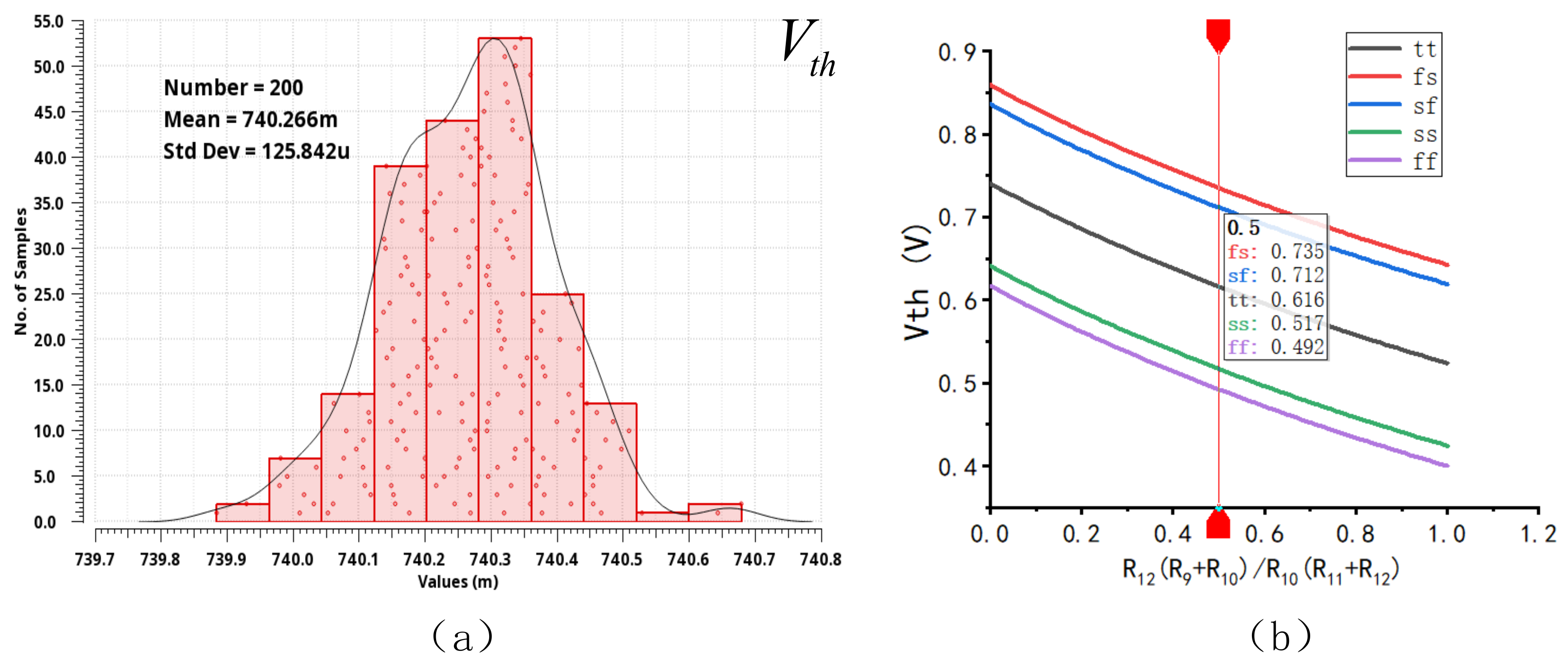
Figure 9a shows the Monte Carlo simulation results of the threshold voltage for a power MOS N-P with an aspect ratio
, a supply voltage of 0.7 V, and a substrate voltage of 0 V. It can be seen that the mean value of this threshold voltage is 740.266 mV.
The circuit structure of the proposed NSUB-REG module is shown in
Figure 10. This module consists of three parts: the supply voltage detection unit VDD-SENSOR, the level conversion unit LEVEL-SHIFT, and the clamp unit CLAMP. VDD-SENSOR detects whether
meets the conditions that can make M72 turn on, LEVEL-SHIFT determines the voltage value of NSUB according to the output result of VDD-SENSOR, and the CLAMP unit clamps the substrate voltage NSUB of N-P to the set value when VDD is smallerlow. When
the drain current in M72
, M71 operates in the deep triode area, the drain voltage of M71 is probably VDDhigh and L78D will be probably
low, which makes the substrate voltage of N-P
. At this time, the gate input voltage
of M85 in CLAMP can be expressed as shown in Equation (
4), where
is the gate source-voltage of M84. Since
, the gate input voltage
of M88 can be expressed as shown in Equation (
5).
According to the feedback effect, eventually we can obtain
. The expression of NSUB at supply voltage
can be obtained as shown in Equation (
6). According to Equation (
3), the threshold voltage of N-P at this time is shown in Equation (
7). From Equations (
2) and (
7), we find that
, so the threshold voltage of N-P can be reduced. The threshold voltage of N-P can be changed by adjusting the value of
. The simulation results of the thresholds of N-P at different craft corners for different
are shown in
Figure 9b, where
. In the design of NSUB-REG, the final choice is
.
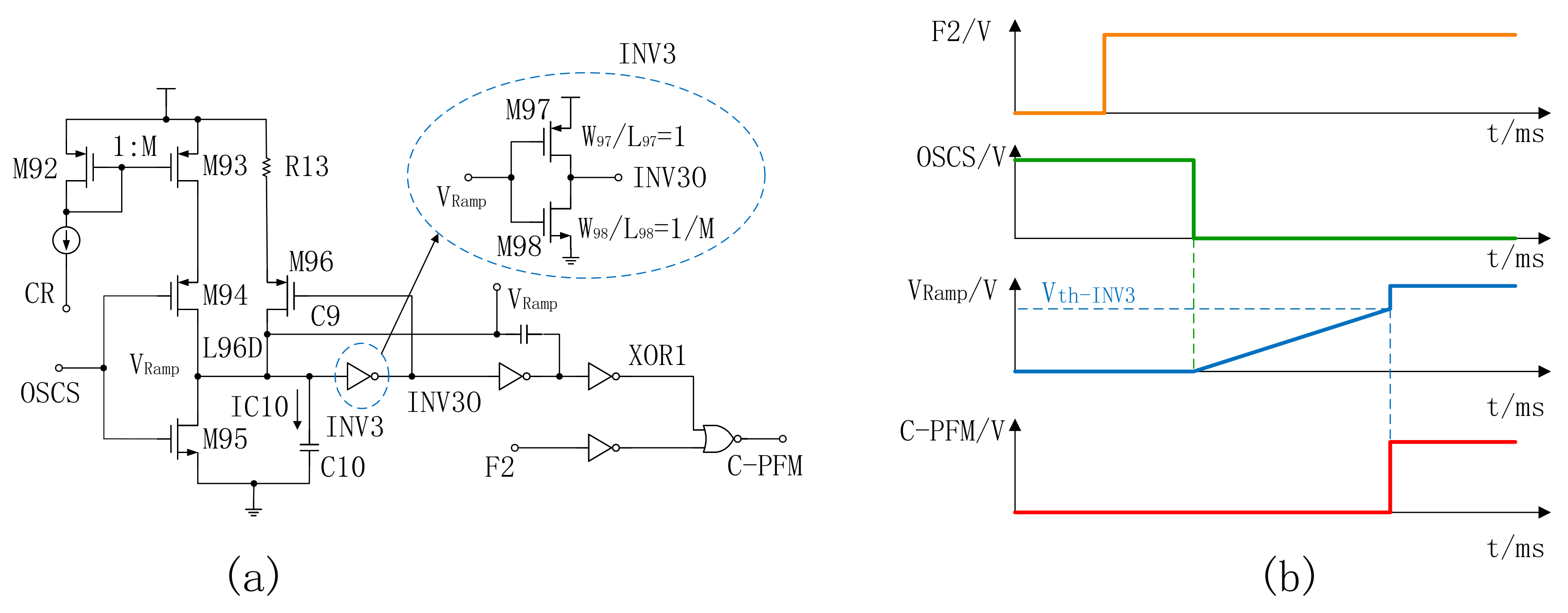
3.4. V-Ramp
Figure 11a shows the circuit structure of the proposed V-Ramp-G module, which not only generates the ramp voltage
for the soft-start stage, but also generates the C-PFM signal that controls the PFM conduction when the soft-start is finished. When C-PFM is probably
, the PFM module starts to work normally. F2 is the output signal of VIO-CMP, and F2 is high at
. C-PFM is high only when both F2 is
and INV3O is
In
Figure 11(a), the aspect ratio of M97 in inverter INV3 is
, and the aspect ratio of M98 is
, so INV3O can be flipped from high to low only when
reaches a large value expressed as
.
Figure 11b shows the logical relationship between F2, OSCS,
, and C-PFM at the ideal state.
4. Experimental Results
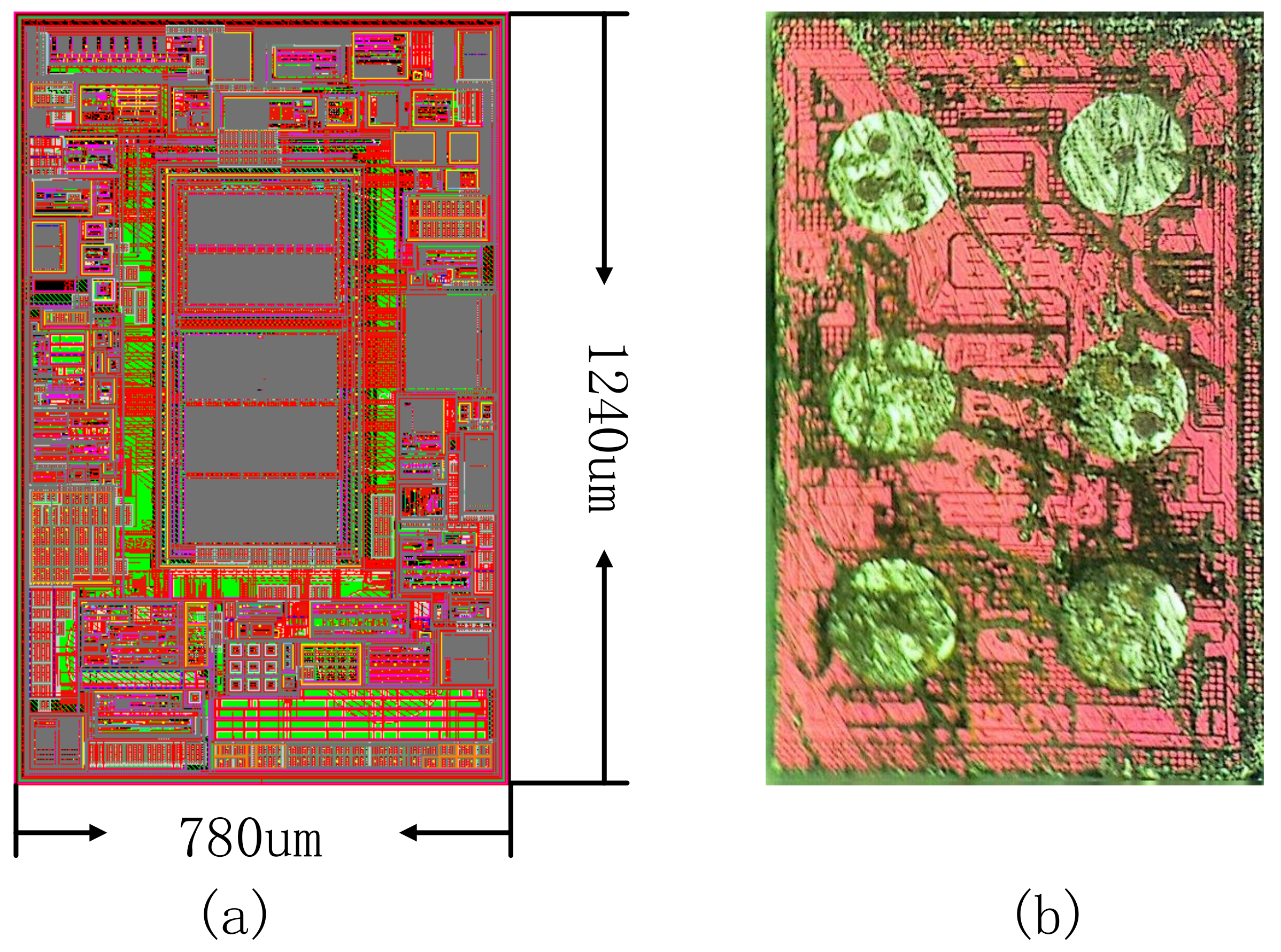
This chip is fabricated by 0.18 um CMOS process, and the layout design of this chip is shown in
Figure 12a, and the observation of this chip under the microscope is shown in
Figure 12b, where the area of this chip is 1240
m × 780
m.
Figure 13 shows a picture of the test bench of the boost converter and the PCB board used for measurement. The off-chip inductor L = 2.2 uH, off-chip input capacitor
= 10 uF, and off-chip filter capacitor
= 20 uF.
Figure 14 shows the experimental results of the start-up process of this boost converter.
Figure 14a shows the start-up process of this boost converter at an input voltage of 0.7 V and a load current of 1 mA, and the results are consistent with the theoretical analysis. At an input voltage of 0.7 V, a load current of 1 mA is a heavy load for the boost converter, which operates in PWM mode at phase (5).
Figure 14b,c show the start-up process of the boost converter at the input voltage
= 3.6 V, which differs slightly from the theoretical analysis. This difference is that the starting process can be further divided into starting under light load conditions and starting under heavy load conditions.
Figure 14b shows the start-up process at light load for
= 3.6 V,
= 50 mA, which remains consistent with the theoretical analysis. The boost converter goes into PFM mode at stage (3) because the load current is low.
Figure 14c shows the start-up process at
= 3.6 V,
= 200 mA, which means that the boost converter is in a heavy load situation.
Figure 14c differs from
Figure 14b in that although
at stage (1), the on-current of the parasitic diode is less than the load current
, resulting in the output voltage of the boost converter not rising. It is not until
that the on-state current of the parasitic diode starts to be greater than the load current
, and the boost converter enters stage (2), resulting in the output voltage
starting to rise. The phase (4) soft start is finished and the boost converter operates in PWM mode. The experimental results show that the output voltage
and the inductor current
of the boost converter do not overshoot under any of the abovementioned start-up conditions, and a stable start-up of the boost converter can be achieved.
Figure 15 shows the experimental results of the output voltage
, inductor terminal voltage
and inductor current
for stable operation of the boost converter at input voltage
= 3.6 V. The load current
= 30 mA in
Figure 15a, when the boost converter is operating in PFM mode, the operating frequency of the boost converter is 300 KHz, the inductor has a peak value of 330.5 mA, and the ripple of the output voltage is 15.6 mV. In
Figure 15b, the load current
= 200 mA, and when the boost converter is operating in PWM mode, the operating frequency of the boost converter is 1.456 MHz, the inductor has a peak value of 596 mA, and the ripple of the output voltage is 7.4 mV.
The experimental results of the load switching response of the proposed boost converter are shown in
Figure 16.
Figure 16a shows the experimental results of the output voltage VOUT when the load current
is switched between 10 mA and 50 mA at the input voltage
= 1.5 V. The response time of the boost converter is 52.4 us when the load current
is switched from 50 mA to 10 mA, and the voltage up-shoot is 45.2 mV. The response time of the boost converter when
switches from 10 mA to 50 mA is 45.4 us, and the voltage down-shoot that occurs is 42.6 mV.
Figure 16b shows the experimental results when the load current is switched between 50 mA and 250 mA at an input voltage of 3.6 V. The response time of the boost converter is 42.4 us when the load current
is switched from 250 mA to 50 mA, and the voltage upsurge is 30.2 mV. The response time of the boost converter when
switches from 50 mA to 250 mA is 40.8 us, and the voltage down-shoot that occurs is 32.4 mV.
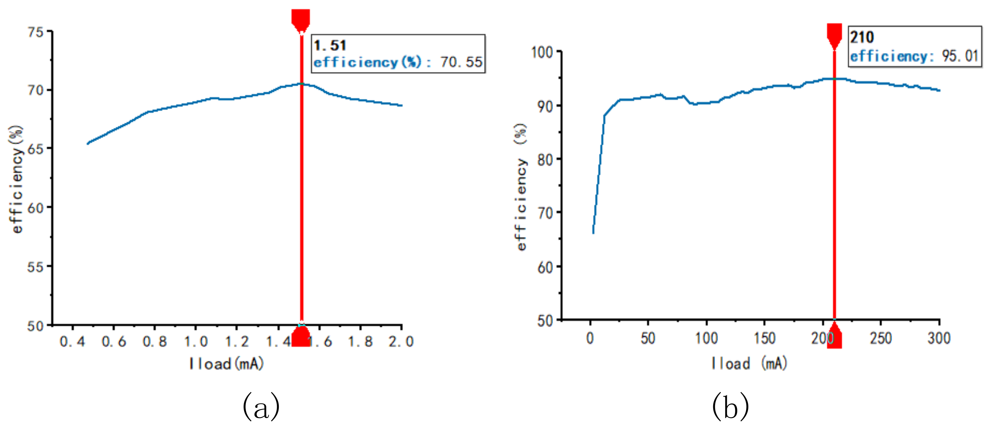
The efficiency test results of the proposed boost converter are shown in
Figure 17, where the maximum load current is 2 mA at 0.7 V and 300 mA at 3.6 V input voltage when the converter can start smoothly and stabilize at 5 V output voltage.
Figure 17a shows the experimental results of the efficiency of the boost converter at an input voltage of 0.7 V and a load current
[0 mA, 2 mA]. It can be seen that the maximum efficiency of the boost converter can be achieved at 70.55% at a load current of 1.53 mA.
Figure 17b shows the experimental results of the efficiency of the boost converter at an input voltage of 3.6 V and a load current of
[0 mA, 300 mA]. It is known that the maximum efficiency of the boost converter is 95.01% when the load current is 210 mA.
Table 1 shows the comparison of the proposed synchronous boost converter with the existing near-threshold start synchronous boost converter. Devices with lower threshold values (threshold voltages of 0.42 V and 0.45 V, respectively) were used in the proposed boost converters in Refs. [
31,
32]. Although starting at lower voltages can be achieved, the starting voltage still needs to be greater than the threshold voltage for the boost converter to start properly. However, the proposed boost converter in this paper uses a novel staged start-up and threshold voltage regulation technique to achieve stable start-up with an input voltage about 40 mV below the threshold voltage when a conventional process device (threshold voltage of 0.74 V) is used. Additionally, it has a higher output voltage, higher efficiency, and larger input voltage and load current range.


