Article

Polymorphic Hybrid CMOS-MTJ Logic Gates for Hardware Security Applications

Innovative Technologies Laboratories (ITL), King Abdullah University of Science and Technology (KAUST), Thuwal 23955-6900, Saudi Arabia
*
Author to whom correspondence should be addressed.
Electronics 2023, 12(4), 902; https://doi.org/10.3390/electronics12040902
Submission received: 3 December 2022 / Revised: 22 January 2023 / Accepted: 7 February 2023 / Published: 10 February 2023

Abstract

:
Various hardware security concerns, such as hardware Trojans and IP piracy, have sparked studies in the security field employing alternatives to CMOS chips. Spintronic devices are among the most-promising alternatives to CMOS devices for applications that need low power consumption, non-volatility, and ease of integration with silicon substrates. This article looked at how hardware can be made more secure by utilizing the special features of spintronics devices. Spintronic-based devices can be used to build polymorphic gates (PGs), which conceal the functionality of the circuits during fabrication. Since spintronic devices such as magnetic tunnel junctions (MTJs) offer non-volatile properties, the state of these devices can be written only once after fabrication for correct functionality. Symmetric circuits using two-terminal MTJs and three-terminal MTJs were designed, analyzed, and compared in this article. The simulation results demonstrated how a single control signal can alter the functionality of the circuit, and the adversary would find it challenging to reverse-engineer the design due to the similarity of the logic blocks’ internal structures. The use of spintronic PGs in IC watermarking and fingerprinting was also explored in this article. The TSMC 65nm MOS technology was used in the Cadence Spectre simulator for all simulations in this work. For the comparison between the structures based on different MTJs, the physical dimension of the MTJs were kept precisely the same.

1. Introduction

The remarkable rise of embedded systems in recent years has led to the globalization of custom integrated circuit (IC) design. With the development of semiconductor technology scaling to very deep submicron levels, the cost of manufacturing these devices has significantly grown. Therefore, only some semiconductor organizations can handle the entire supply chain, from design to packaging. Most of the remaining companies have given up on the fabrication process and depend on unreliable foundries to produce their ICs [1]. Although using a third party’s fabrication facilities can lower costs and shorten time to market, it also raises significant hardware security issues [2]. An untrustworthy and unreliable foundry opens the door to threats such as IP theft, reverse-engineering, counterfeiting, hardware Trojan insertion, overproduction of integrated circuits, and IC cloning [3,4,5,6,7]. Developments have considerably improved the concept of hardware security in various developing technologies, including memristors, nanowire FETs (NWFETs), carbon nanotubes (CNTs), graphene nanocarbon (GNR), and spintronic devices [8,9,10,11,12,13]. Nanodevices’ numerous inductive and capacitive effects are also thoroughly investigated for the on-chip interconnects [14,15,16,17,18]. Numerous spintronics phenomena have been studied, including all-spin logic, spin–torque clocking, voltage-controlled magnetic anisotropy, current-induced spin accumulation, and usage in a range of applications, including logic circuits, memories, flexible electronics, terahertz emitters, and quantum computer circuits [19,20,21]. These devices have a variety of characteristics, including non-volatility, low power consumption, high durability, and high circuit integration density, which are advantageous for hardware security and in-memory computing. Researchers have investigated the usage of spintronic devices for hardware security primitives such as hardware Trojans, physically unclonable functions (PUFs), true random number generators (TRNGs), and logic locking [22,23,24,25,26,27]. A. Stoica first proposed a unique reconfigurable method based on PGs in 2001 [28]. Polymorphic gates/circuits can perform function transformation in response to control factors such as temperature, supply voltage, and external inputs because multiple functionalities are integrated into a single structure. Spintronics-based polymorphic and reconfigurable logic is also emerging as a potential method to increase the hardware’s security [29,30,31,32,33,34,35].
This work proposes the use of logic-in-memory architecture-based spintronic PGs for hardware security primitives, such as preventing manufacturing-time tampering, watermarking, and fingerprinting in integrated circuits. The rest of the paper is organized as follows. Section 2 discusses the background of magnetic tunnel junctions and the logic-in-memory architecture. Section 3 demonstrates the operation of PGs and their use in hardware security applications. The experimental results and challenges are discussed in Section 4. The paper is finally concluded in Section 5.

2. Background

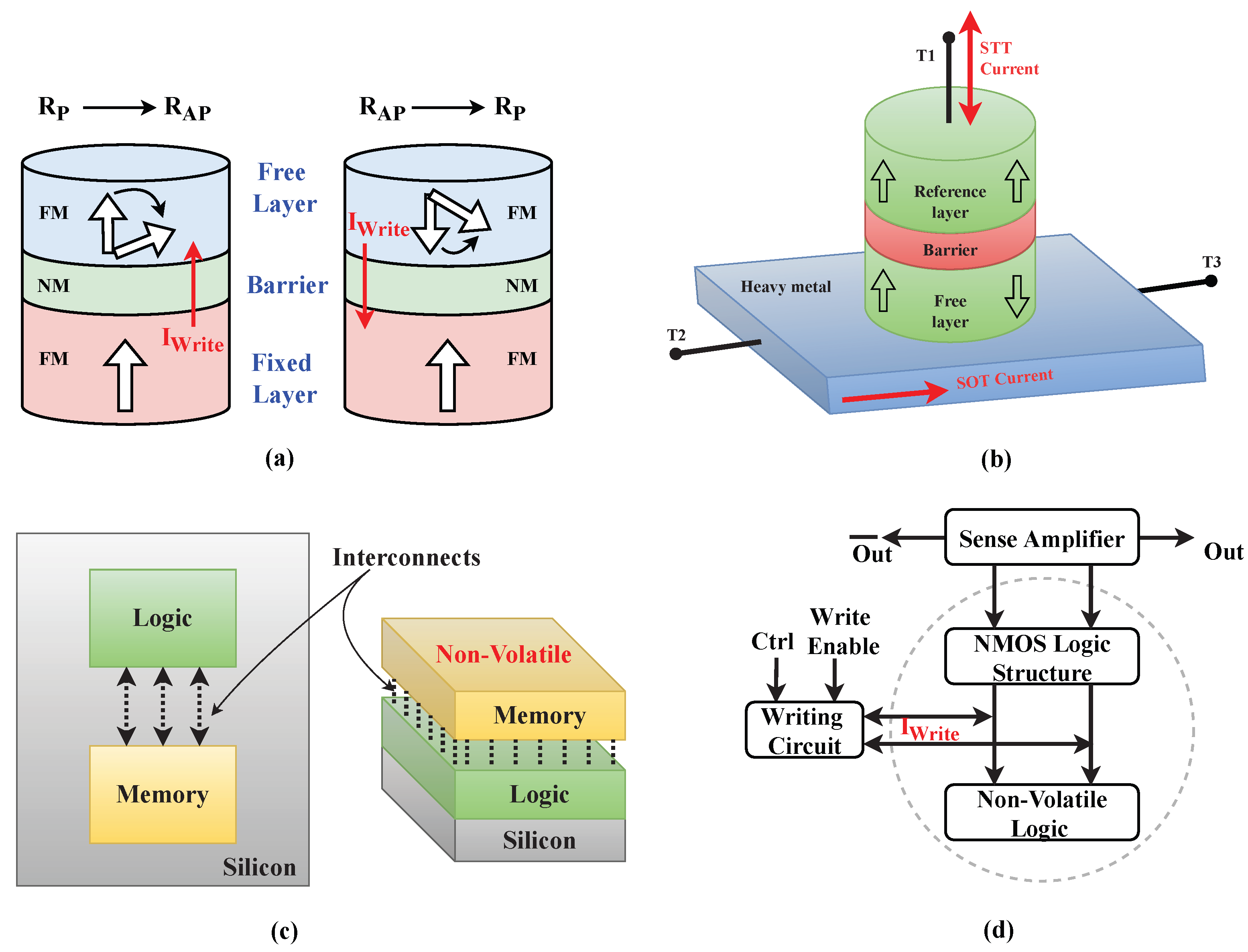
2.1. Magnetic Tunnel Junction: Construction and Switching

A magnetic tunnel junction is a multilayer nano-stack structure of two ferromagnetic (FM) layers and an oxide layer. One of the FM layers in the MTJ stack has a fixed magnetic orientation and is referred to as a fixed/reference/pinned layer. The other layer is known as a free layer, and its magnetic orientation can be either similar to or opposite that of the pinned layer. Multiple MTJ devices with two and three terminals have been explored that utilize various mechanisms such as spin-transfer torque (STT), spin–orbit torque (SOT), and voltage-controlled magnetic anisotropy (VCMA) for switching. Perpendicular magnetic tunnel junctions (p-MTJs) are preferred over in-plane magnetic tunnel junctions (i-MTJs) due to their longer retention durations, lower power dissipation, improved thermal stability, ease of scaling, and several other advantages. The structure of a two-terminal p-MTJ using the spin-transfer torque effect for switching [36] is shown in Figure 1a. In this phenomenon, a charge current is passed through the MTJ stack, which becomes spin-polarized while crossing through the FM layers and results in the switching of the magnetic orientation of the free layer. When both FM layers have the same magnetic orientation, this state is parallel (P), and the MTJ offers a lower resistance, whereas it offers higher resistance when the magnetic orientations of the two FM layers are opposite, a condition known as an antiparallel state (AP). Resistance in parallel and antiparallel states is indicated by the symbols R P and R A P . In a three-terminal MTJ, the stack of MTJs is fabricated on a heavy metal layer [37], as shown in Figure 1b. A charge current is used to alter the MTJ’s state by passing it via the heavy metal layer, which exerts a torque on the free layer and aids in switching the state. This heavy metal layer increases the area of the overall device; since lower current is passed through the oxide barrier, the device has more endurance. Tunnel magnetoresistance (TMR), which is computed as follows, describes the relative resistance variation between parallel and antiparallel states:
T M R = R A P R P R P × 100
In the macrospin approximation, a modified Landau–Lifshitz–Gilbert (LLG) equation governs the magnetization dynamics of the free layer [37], as
m t = γ μ 0 m × H e f f + α m × m t ξ P J S T T m × ( m × m r ) ξ η J S H E m × ( m × σ S H E )
Here, m and m r are the unit vector along with the magnetization of the free layer and the reference layer, respectively, γ is the gyromagnetic ratio; μ 0 is the vacuum permeability; H e f f is the effective magnetic field; α is the Gilbert damping coefficient; P is the polarization factor; J S T T and J S H E are the STT and SOT current density applied to the MTJ device; σ S H E is the polarization direction of the spin current injected in the free layer.

2.2. Logic-in-Memory Architecture

The von Neumann architecture has been used for many years in CMOS technology for IC manufacturing. The control unit, memory unit, registers, and inputs/outputs are the components of this architecture that communicate through wires and interconnects [38]. The von Neumann bottleneck—a limited throughput between the central processor unit and memory compared to the amount of memory—is caused by the shared bus between the program memory and data memory. In order to minimize the delay brought on by cables and interconnects, the LIM architecture is an emerging concept. Figure 1c illustrates how non-volatile devices are arranged over a logic circuit plane and positioned close to one another in this layout. This memory integration on top of the logic reduces the overall area occupied and shortens the length of wires and interconnects.
A hybrid CMOS-MTJ approach-based the LIM architecture is shown in Figure 1d. The three components of this LIM architecture are the sense amplifier, the logic structure, and the writing circuit. The output of the circuits, which varies with the input sequence in the NMOS logic structure and the data present in the non-volatile logic, is sensed by the sense amplifier. The precharge sense amplifier (PCSA) [39], offset-compensated high-speed sensing (OCHS) [40], dynamic dual-reference sensing (DDRS) [41], latch offset cancellation sensing (LOC) [42], double switches and transmission gate access transistor sensing (DSTA) [43], and high-sensing margin, high-speed, and stability sensing (HMSS) [44] are amongst the current mode sensing circuits that have been investigated for STT-MRAMs. The data stored in the non-volatile logic are changed using the writing circuit. A bidirectional current is passed through the MTJ stack in the case of STT-MTJs, whereas in the case of SOT-MTJs, a larger write current is passed through the heavy metal layer and a small STT current is passed through the MTJ stack. The writing circuit with four transistors can write one, as well as two MTJs connected in series [36,45].

3. Proposed Work: Spintronics PGs for Hardware Security Applications

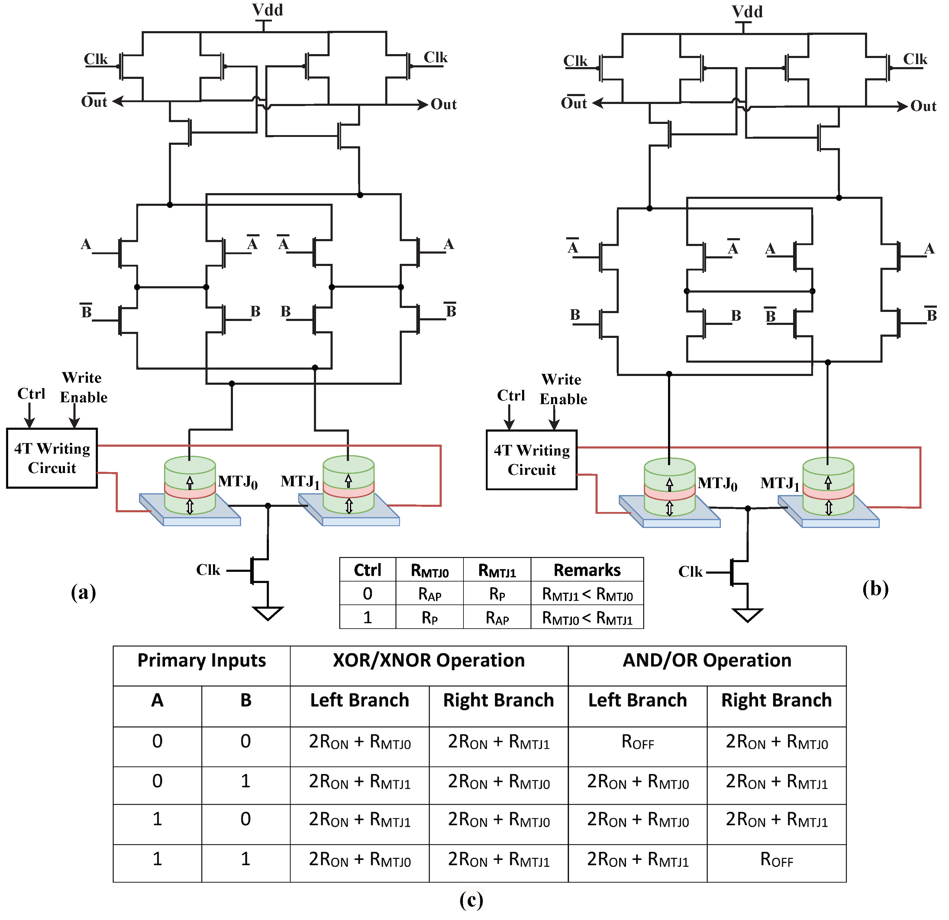
3.1. Operation of Spintronics PGs

The ability of PGs based on spintronics to improve hardware security was investigated in this work. In hybrid CMOS-MTJ circuits, the circuit can carry out various operations depending on the resistance of the complementary MTJs. The NMOS logic structures proposed in [46] were utilized in this work; however, the investigation also included the three-terminal SOT MTJs in addition to the two-terminal STT MTJs. For a better comparison, both types of MTJs have exactly matching physical dimensions and several other factors, as listed in Table 1. The hybrid CMOS-MTJ-structure-based circuits utilizing three-terminal MTJs as non-volatile logic are shown in Figure 2. Precharge sense amplifiers were employed in this work to sense the circuit’s outputs. In these circuits, two MTJs are present with free layers magnetized in opposite directions, offering different resistance to the current. A four-transistor-based writing circuit changes the state of the MTJs by sending a control signal (Ctrl). The write enable signal must be turned to high for the Ctrl signal to function.
The circuits in Figure 2 operate in two phases. (1) Precharge phase: During this time, the Clk signal is low, activating the Clk-controlled PMOS transistors and charging both outputs to Vdd. (2) Evaluation phase: This stage begins as soon as the Clk pulse changes from low to high, turning on the tail NMOS transistor and opening a path for current to flow to the ground. One of the outputs is discharged completely, making the other output high, depending on the resistance of the left and right branches. The structure always produces complementary outputs, which may be employed depending on the needs of the circuit. When the Ctrl is low, the circuit in Figure 2a performs the XOR operation at the out terminal, and it changes to XNOR when the Ctrl signal is made high. Similarly, the circuit of Figure 2b performs AND and OR logic operations at the out terminal when the Ctrl signal is 0 or 1, respectively. The resistance offered to the PCSA in the left and right branches of the circuits is shown in a table in Figure 2c. Because both outputs are at Vdd during the precharge phase, the one brought down to zero faster in the evaluation phase causes the other output to return to Vdd due to the inverters in the PCSA. The resistance offered by MTJs in the parallel state is lower than the resistance provided in the antiparallel state. By adjusting the tunneling magnetoresistance of the MTJ, this resistance variation, which varies by a few k Ω , can be controlled.

3.2. Preventing Manufacturing-Time Tampering

The idea of hiding functionality utilizes the non-volatile property of MTJs. The symmetrical structures of Figure 2 are valuable for hiding a netlist or layout’s functionality after manufacturing. Being unaware of the specific logical block’s functioning prevents an attacker in the foundry from altering the design. The operation or functionality of these gates can be switched simply by manipulating the state of the MTJs with control signals. The MTJ state can be permanently changed once after fabrication for correct functionality. The logic circuit diagram utilizing hybrid CMOS/MTJ-based PGs is shown in Figure 3a. Depending on the Ctrl signal, the logic’s output expression changes. Figure 3b displays the circuit’s output F = F 1 = ( B ¯ . C ) when the Ctrl signal is “0”, and Figure 3c displays the circuit’s output when the Ctrl signal is “1”, which is F = F 2 = ( B ¯ + C ) . As a result, the adversary is constrained from making malicious changes to the circuit because he/she does not know how the circuit works. A single writing circuit can also write all of the circuit’s logical blocks to enable control over a single Ctrl input. If a designer wants to employ the same type of block as the AND and OR logic operation at Ctrl = 0 or Ctrl = 1, the connections of the writing circuit must be made in accordance with that. In Figure 2b, the circuit functions as an AND logic when Ctrl = 0. The same circuit can function as an OR operation at Ctrl = 0 by connecting the writing circuit and primary circuit in reverse. Therefore, the operation of the entire circuit can be controlled by a single Ctrl input. However, keeping fewer control signals also increases the probability of an adversary discovering the functionality. The adversary can reveal the functionality with a 50% probability for a single control signal, which lowers as the number of control signals grows. For hiding functionality, it is also taken into consideration that distinct logical operations have similar structures and an exactly equal number of transistors. Any logic operation has a circuit with a similar structure, which results in a similar physical layout, which may not be possible with current CMOS technology. The symmetry of the layouts makes it difficult for an adversary to reverse-engineer a layout after fabrication or even at the fabrication level to determine its functionality.

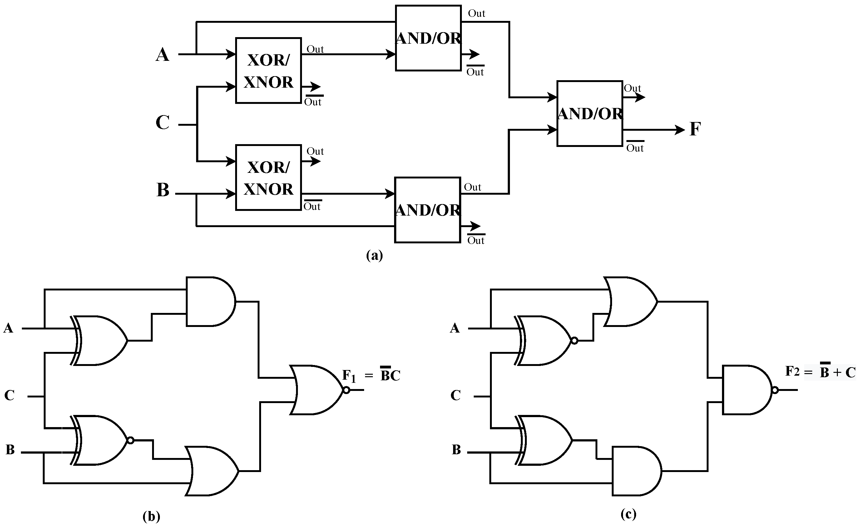
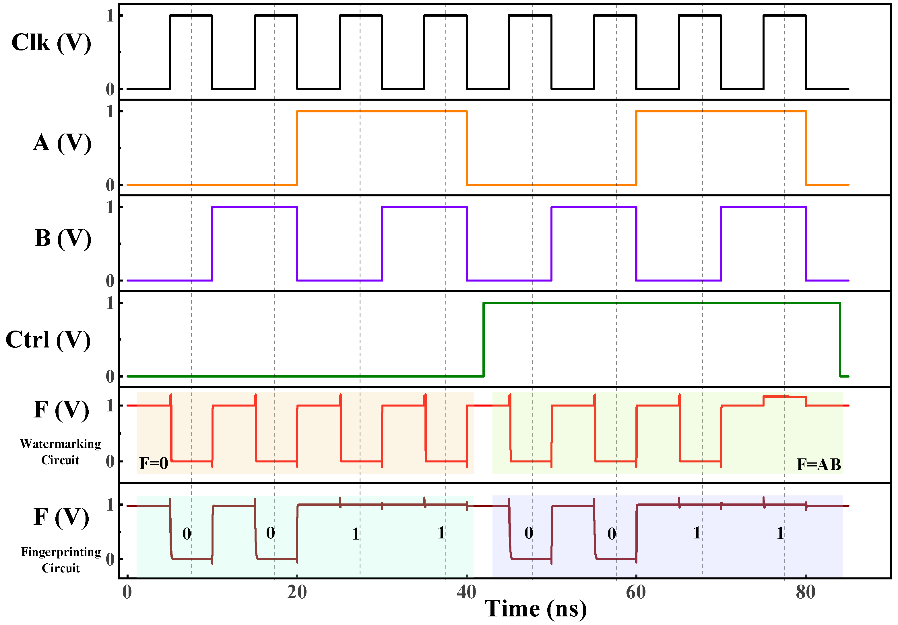
3.3. IC Watermarking

Watermarking is a method that enables the IP designer to hide authorship information inside the design without compromising the design’s functioning [47]. The researchers in [48] reported the use of PGs for IC watermarking techniques. Spintronics-based PGs hold their functionality until the state of the MTJs is changed. Therefore, they can be used in watermarking techniques, as depicted in Figure 4a. In this technique, when the Ctrl signal is set to “0”, the circuit operates appropriately in normal mode, as shown in Figure 4b.
When it is essential to illustrate the watermark, the circuit is switched to the specific mode by setting the Ctrl signal to “1”, as shown in Figure 4c. MTJs offer non-volatile properties; therefore, when used in normal mode, they can retain their state for a longer duration. A PG can replace every cell in the original netlist; however, researchers have developed various algorithms to find a suitable replacement location that ensures that the circuit functions correctly at normal operation after the gates in the location are replaced [48,49]. Additionally, the functionality of the modified circuit in normal and special modes can be differentiated by observing the primary outputs.

3.4. IC Fingerprinting

Circuit fingerprinting is a technique for adding special characteristics to each copy of a circuit so that they can be recognized and traced to stop intellectual property (IP) piracy. Spintronics-based PGs can replace the standard library cells holding the satisfiability don’t care (SDC) conditions. SDC conditions describe the logic combinations that will not occur in the internal nets, given all the combinations that the primary inputs can take [50]. The configurations of the PGs serve as the circuit fingerprint and ensure that the modified circuit operates as intended. In Figure 5a, the input to AND/OR block is always (0,0) and (1,1). The other combinations do not exist at the input of the block; the same can be seen from the table in Figure 5b. Therefore, an AND/OR PG can be used at the location because that will not affect the functionality. Due to the non-volatile characteristics of MTJs, spintronics-based PG can be fabricated with a certain orientation of MTJs and without connections to the writing circuit, allowing for the use of the devices as dummy fingerprints. Since fingerprinting is an infrequent event, after the fingerprinted copies of the original circuit are fabricated, the configuration type of the PG can be determined by opening the chip to find embedded fingerprints. The attacker can change the fingerprint of these PG to a fingerprint that the manufacturer has not distributed. However, this attack necessitates locating the dummy fingerprint bits, as altering these would affect the circuits’ operation.

4. Results and Discussion

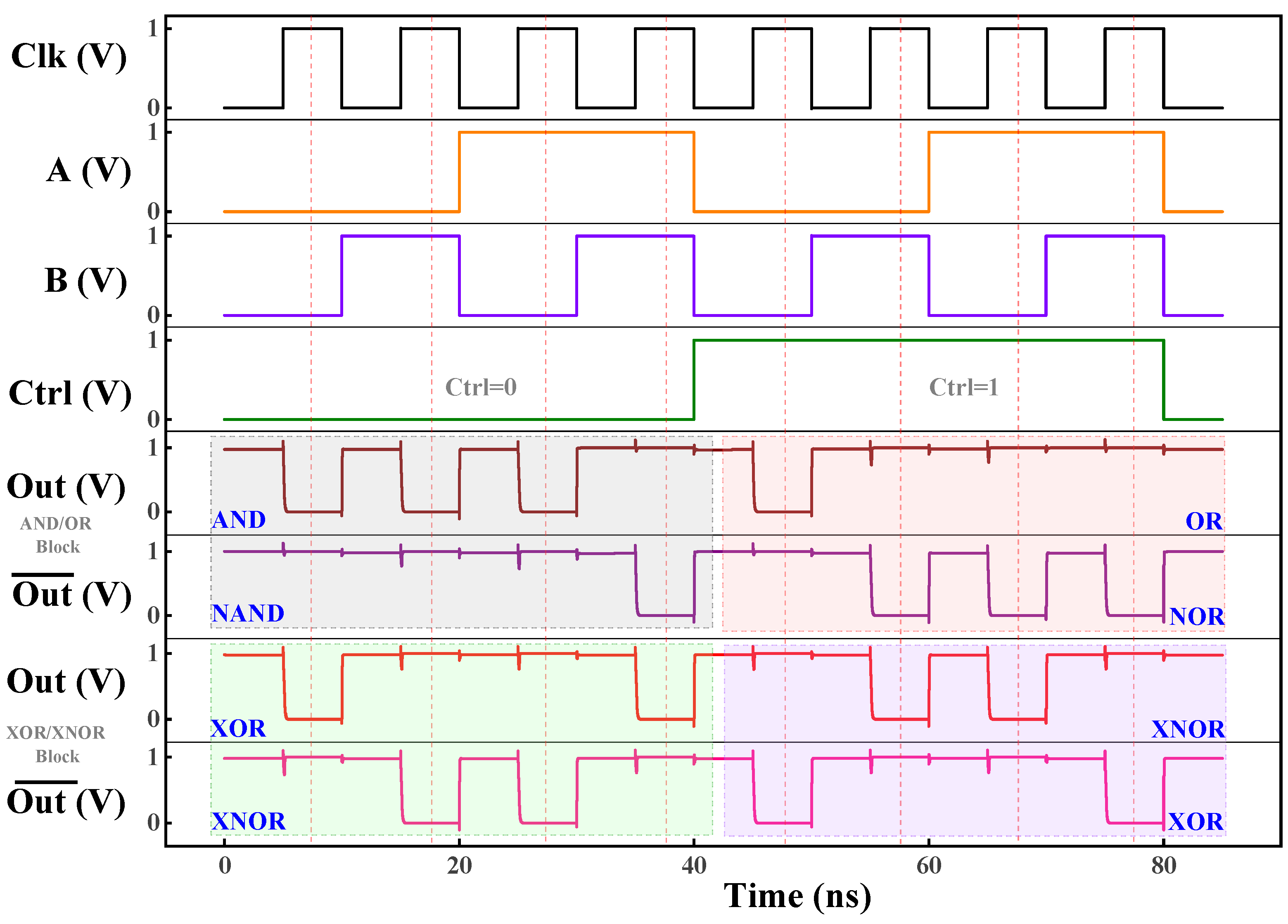
4.1. Simulation Results

Figure 6 displays the output waveform for the circuits indicated in Figure 2, where the polymorphic behavior of the circuits in response to a control signal can be seen. The output of the AND/OR circuit, where the AND operation shifts to the OR operation as the Ctrl signal changes from 0 to 1, is represented by the first out curve in the figure. Similar to this, the second out curve in the diagram represents the XOR/XNOR operation at the out terminal, and when the Ctrl signal changes from negative to positive, the operation shifts from XOR to XNOR. The TSMC 65 nm MOS technology node was used for the MOS transistors with l = 60 nm and w = 200 nm for both NMOS and PMOS transistors. The simulations were run using the parameters listed in Table 1 in the Cadence Spectre simulator.
The circuits of Figure 2 were simulated with both two-terminal and three-terminal MTJ structures, with the Verilog A-based behavioral models of MTJs, mentioned in Table 1. The various parameters, including the physical dimensions of both the STT and SOT-MTJ stack, were kept equal for a better comparison. The circuit uses a precharge sense amplifier, which charges both output terminals to “1” when the clock pulse is low; thus, there is no rise time for the outputs. A four-transistor-based writing circuit was used for writing the state of the MTJs [45]. Table 2 lists the maximum fall time and delay observed in each operation. The fall time was calculated by considering the curve’s start and end points at 90% and 10% of their maximum, respectively, and Vdd as 1V. From the table, it can be seen that, in most cases, the STT-MTJs performed faster than the SOT-MTJs. However, the write current is not passed through the stack in the SOT-MTJs, so the device’s endurance was better. The O u t / O u t ¯ signal and the 50% level of the Clk signal determined the delay. The size of the MOS transistors can be increased to reduce the delay further. Figure 7 illustrates that the delay of the SOT-based XOR and NAND operations decreased with the increasing tail NMOS transistor width in the PCSA. STT-MTJ-based logical operations offered a significant difference in the propagation delay. This raises the likelihood that the operation will be detected. The power consumption of SOT-MTJ-based logical operations was calculated due to the similar delays of various operations. The results showed that the AND/NAND, OR/NOR, and XOR/XNOR each utilized 1.93 μ W, 1.95 μ W, and 2.41 μ W, respectively. However, this does not include the power consumed by the writing circuit since one writing circuit can be utilized for multiple logic blocks. The writing circuit consumed approximately 18 μ W of power when the SOT-MTJ-based logic operations were performed. The comparable delay and power of various operations provide an advantage for preventing the circuit from side-channel attacks. The SOT-based PGs should always be chosen for applications where the circuits will constantly be in use. However, both SOT- and STT-based PGs can be utilized for infrequent events such as fingerprinting and watermarking.
The output waveforms for the sample circuit for watermarking utilizing STT-MTJs and fingerprinting utilizing SOT-MTJs are plotted in Figure 8. The same input combinations were used for both logic circuits. The functionality of both circuits can be observed from the waveform. As the PGs use the clock signal, the MOS logic gates in the sample circuit were based on the dynamic CMOS logic. The output of the dynamic logic may exceed the supply voltage as a result of issues including clock-feedthrough and capacitive coupling [51].

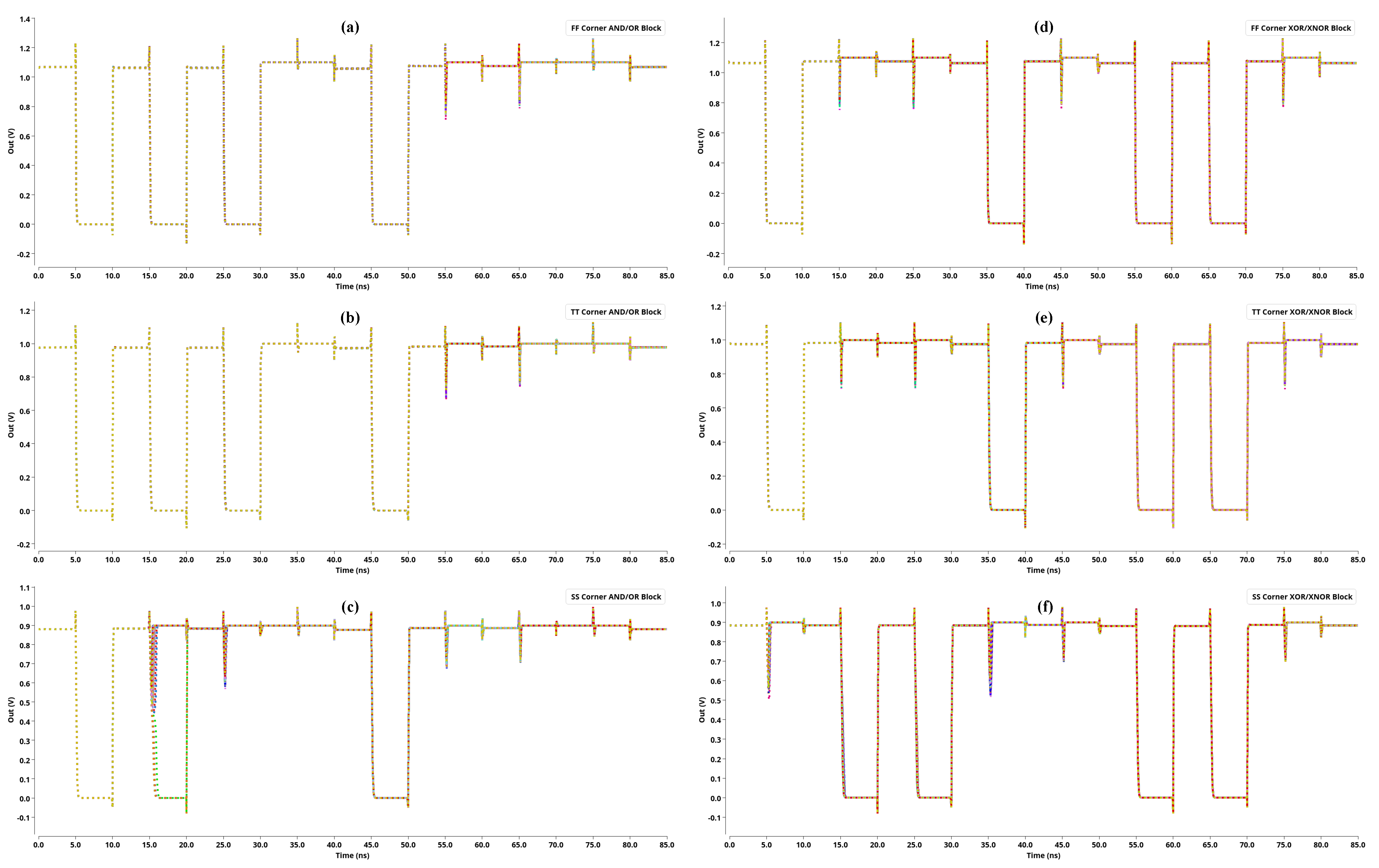
4.2. Effect of Process Variation

With a maximum 3% variation in certain MTJ parameters that follow a Gaussian distribution, Monte Carlo simulations were performed for different corners of the MOS transistors. These MTJ parameters included TMR, the free-layer thickness, the oxide layer thickness, and the device surface. The low-discrepancy sequence (LDS) method, which uses a deterministic sequence to provide uniform coverage of the sample space, was used in the Monte Carlo simulation. Its convergence accuracy ≈1 / p o w ( N , 2 / 3 ) was faster than the random sampling method, which had a convergence accuracy of 1/sqrt (N). The 200-times Monte Carlo simulations were performed in each fast–best (all MOS devices in FF) case, the typical case, and the slow–worst (all MOS devices in SS) case for both AND/OR and XOR/XNOR operation. The data for the same are listed in Table 3. The temperature variation was applied based on the manual of the technology node, and a 10% variation was applied in the supply voltage with respect to the typical case. The simulation showed that the circuits operated correctly at the fast–best and the typical corner, but the operation was disturbed at the slow–worst corner. The primary reason for the operation error was the voltage across the MTJs. With 0.9V supply voltage, the MTJs needed to receive more current for proper switching. The waveform in Figure 9 represents the voltage at the out terminal of both circuits in the above-mentioned process corners.

4.3. Design Considerations, Discussion, and Challenges

Several design constraints should be considered while designing MTJ-based circuits for these applications. Polymorphic circuits based on MTJs are susceptible to the loading effect since the circuits’ ability to operate depends on the MTJ resistance. According to the TMR value and the dimensions, the resistance difference between the two branches during sensing operation is a few k Ω . The operation could become unstable if other circuit components heavily load the system. MTJs ought to have a high tunnel magnetoresistance because of this. The retention period is another factor. It is important to choose MTJ parameters that have a long-enough retention time. According to the industry standard, the retention period for non-volatile memories should be ten years [52]. The retention time of MTJs is described by the thermal stability factor, which should be high to ensure that MTJ’s condition is resistant to external thermal fluctuation. In the macrospin area, the thermal stability factor is constant with respect to the MTJ size, but it responds linearly to the lateral diameter below the subvolume limit [36]. A periodic write operation should be performed in the writing circuit if the MTJs’ retention time is significantly lowered. The writing circuit should have sufficient driving power to simultaneously write the states of all MTJs if the designer employs a single writing circuit for all blocks. Table 4 summarizes earlier efforts to build polymorphic gates utilizing spintronic devices. The table contains information on the employed devices and the morphing techniques. The spintronic-based polymorphic gates’ power, area, and delay were much higher than standard CMOS logic circuits. Compared to the standard CMOS AND gate and OR gate, the transistor count was larger by nine transistors and two MTJs and by seven transistors and two MTJs for the XOR and XNOR gates. Writing circuitry is also necessary for writing the state of MTJs. Compared to the power usage of typical CMOS gates and STT-MTJ-based PG [46], which is of the nW order, the power consumption of SOT-based PGs is several μ W. A typical CMOS gate in the same technological node has a maximum delay of approximately 40 ps, significantly lower than spintronics gates. These are challenges that SOT-MTJ-based circuits must overcome as the field of spintronics develops. Along with this, the operation of the circuits at various process corners of the MOS technology nodes should be appropriately tested.

5. Conclusions

This article analyzed how spintronics-based polymorphic gates can be used to construct logic circuits that conceal a circuit’s functioning and guard against tampering during manufacturing by taking advantage of magnetic tunnel junctions’ non-volatile property. Other hardware security applications, such as integrated circuit watermarking and fingerprinting, can benefit from using these polymorphic gates. In order to prevent an adversary at the foundry from tampering with the design, the correct functionality of a circuit can be attained by writing the MTJ state only once after fabrication. If the MTJ’s retention time is sufficient, no periodic writing is necessary, and just one writing circuit with a very high driving capability is needed to write several blocks at once. The TMR and MTJ size should be selected appropriately when building such circuits to reduce the loading effect from other circuit components. The comparable power and delay of various operations in SOT-MTJ-based circuits will make it challenging to identify the operation using side-channel analysis. The equal transistor and MTJ count, along with a similar structure for various operations, can lead to a similar physical layout, which will be advantageous when the opponent is performing reverse-engineering or determining functionality from the physical layout. Many design-related issues and challenges, including high power, area, delay, and low fan-out, will need to be solved in the future. This opens the door to investigating more MTJ structures with sub-10 nm dimensions.

Author Contributions

Conceptualization, R.K.; methodology, R.K. and D.D.; software, R.K. and D.D.; validation, R.K., D.D., D.K. and Y.M.; formal analysis, R.K.; investigation, R.K., D.D. and D.K.; resources, D.K., S.A. and Y.M.; data curation, R.K. and D.D.; writing—original draft preparation, R.K. and D.K.; writing—review and editing, D.K.; visualization, R.K. and D.D.; supervision, Y.M.; project administration, Y.M.; funding acquisition, Y.M. All authors have read and agreed to the published version of the manuscript.

Funding

This research received no external funding.

Institutional Review Board Statement

Not applicable.

Informed Consent Statement

Not applicable.

Data Availability Statement

Data sharing is not applicable to this article.

Conflicts of Interest

The authors declare no conflict of interest.

References

  1. Semiconductor Industry Association. Available online: https://www.semiconductors.org/ (accessed on 8 February 2023).
  2. Guin, U.; Forte, D.; Tehranipoor, M. Anti-counterfeit techniques: From design to resign. In Proceedings of the IEEE 14th International Workshop Microprocessor Test Verification, Austin, TX, USA, 11–13 December 2013; pp. 89–94. [Google Scholar]
  3. Tehranipoor, M.; Guin, U.; Forte, D.; Tehranipoor, M.; Guin, U.; Forte, D. Counterfeit integrated circuits. In Counterfeit Integrated Circuits; Springer: Cham, Switzerland, 2015; pp. 15–36. [Google Scholar]
  4. Kumar, R.; Divyanshu, D.; Khan, D.; Amara, S.; Massoud, Y. Spin orbit torque-assisted magnetic tunnel junction-based hardware Trojan. Electronics 2022, 11, 1753. [Google Scholar] [CrossRef]
  5. Bhunia, S.; Tehranipoor, M. Hardware Security: A Hands-on Learning Approach; Morgan Kaufmann: Oxford, UK, 2018. [Google Scholar]
  6. Tehranipoor, M.; Salmani, H.; Zhang, X.; Wang, M.; Karri, R.; Rajendran, J.; Rosenfeld, K. Trustworthy Hardware: Trojan Detection and Design-for-Trust Challenges. Computer 2011, 44, 66–74. [Google Scholar] [CrossRef]
  7. Hu, W.; Chang, C.-H.; Sengupta, A.; Bhunia, S.; Kastner, R.; Li, H. An overview of hardware security and trust: Threats, countermeasures, and design tools. IEEE Trans. Comput.-Aided Des. Integr. Circuits Syst. 2021, 40, 1010–1038. [Google Scholar] [CrossRef]
  8. Alasad, Q.; Yuan, J.; Fan, D. Leveraging all-spin logic to improve hardware security. In Proceedings of the on Great Lakes Symposium on VLSI 2017–GLSVLSI ’17, Banff, AB, Canada, 10–12 May 2017. [Google Scholar]
  9. Rajendran, J.; Karri, R.; Wendt, J.B.; Potkonjak, M.; McDonald, N.; Rose, G.S.; Wysocki, B. Nano meets security: Exploring nanoelectronic devices for security applications. Proc. IEEE Inst. Electr. Electron. Eng. 2015, 103, 829–849. [Google Scholar] [CrossRef]
  10. Ghosh, S. Spintronics and security: Prospects, vulnerabilities, attack models, and preventions. Proc. IEEE Inst. Electr. Electron. Eng. 2016, 104, 1864–1893. [Google Scholar] [CrossRef]
  11. Knechtel, J. Hardware security for and beyond CMOS technology. In Proceedings of the 2021 International Symposium on Physical Design, Virtual Event, 22–24 March 2021. [Google Scholar]
  12. Bi, Y.; Gaillardon, P.-E.; Hu, X.S.; Niemier, M.; Yuan, J.-S.; Jin, Y. Leveraging emerging technology for hardware security–case study on silicon nanowire FETs and graphene SymFETs. In Proceedings of the 2014 IEEE 23rd Asian Test Symposium, Hangzhou, China, 16–19 November 2014. [Google Scholar]
  13. Matsunaga, S.; Hayakawa, J.; Ikeda, S.; Miura, K.; Endoh, T.; Ohno, H.; Hanyu, T. MTJ-Based Nonvolatile Logic-in-Memory Circuit, Future Prospects and Issues. In Proceedings of the 2009 Design, Automation & Test in Europe Conference & Exhibition, Nice, France, 20–24 April 2009. [Google Scholar]
  14. Massoud, Y.; White, J. Managing On-Chip Inductive Effects. IEEE Trans. Very Large Scale Integr. (VLSI) Syst. 2002, 10, 789–798. [Google Scholar] [CrossRef]
  15. Massoud, Y.; White, J. Simulation and Modeling of the Effect Substrate Conductivity on Coupling Inductance and Circuit Crosstalk. IEEE Trans. Very Large Scale Integr. (VLSI) Syst. 2002, 10, 286–291. [Google Scholar] [CrossRef]
  16. Ragheb, T.; Massoud, Y. On the modeling of resistance in graphene nanoribbon (GNR) for future interconnect applications. In Proceedings of the IEEE/ACM International Conference on Computer-Aided Design, San Jose, CA, USA, 10–13 November 2008. [Google Scholar]
  17. Massoud, Y.; Nieuwoudt, A. Modeling and Design Challenges and Solutions for Carbon Nanotube-Based Interconnect in Future High-Performance Integrated Circuits. ACM J. Emerg. Technol. Comput. Syst. 2006, 2, 155–196. [Google Scholar] [CrossRef]
  18. Massoud, Y.; White, J. FastMag: A 3-D Fast Inductance Extraction Program for Structures with Permeable materials. In Proceedings of the IEEE/ACM International Conference on Computer-Aided Design, San Jose, CA, USA, 10–14 November 2002; pp. 478–484. [Google Scholar]
  19. Srinivasan, S.; Sarkar, A.; Behin-Aein, B.; Datta, S. All-spin logic device with inbuilt nonreciprocity. IEEE Trans. Magn. 2011, 47, 4026–4032. [Google Scholar] [CrossRef]
  20. Mishra, R.; Yang, H. Emerging Spintronics Phenomena and Applications. IEEE Trans. Magn. 2021, 57, 1–34. [Google Scholar] [CrossRef]
  21. Kulkarni, A.; Bindal, N.; Kaushik, B.K. Quantum Computing Circuits Based on Spin-Torque Qubit Architecture: Toward the Physical Realization of Quantum Computers. IEEE Nanotechnol. Mag. 2019, 13, 15–24. [Google Scholar] [CrossRef]
  22. Wang, X.; Yang, J.; Zhao, Y.; Jia, X.; Qu, G.; Zhao, W. Hardware security in spin-based computing-in-memory: Analysis, exploits, and mitigation techniques. ACM J. Emerg. Technol. Comput. Syst. 2020, 16, 1–18. [Google Scholar] [CrossRef]
  23. Divyanshu, D.; Kumar, R.; Khan, D.; Amara, S.; Massoud, Y. Physically unclonable function using GSHE driven SOT assisted p-MTJ for next generation hardware security applications. IEEE Access 2022, 10, 93029–93038. [Google Scholar] [CrossRef]
  24. Perach, B.; Kvatinsky, S. An Asynchronous and Low-Power True Random Number Generator using STT-MTJ. In Proceedings of the 2020 IEEE International Symposium on Circuits and Systems (ISCAS), Sevilla, Spain, 10–21 October 2020. [Google Scholar]
  25. Divyanshu, D.; Kumar, R.; Khan, D.; Amara, S.; Massoud, Y. Logic locking using emerging 2T/3T magnetic tunnel junctions for hardware security. IEEE Access 2022, 10, 102386–102395. [Google Scholar] [CrossRef]
  26. Divyanshu, D.; Kumar, R.; Khan, D.; Amara, S.; Massoud, Y. Design of VGSOT-MTJ-Based Logic Locking for High-Speed Digital Circuits. Electronics 2022, 11, 3537. [Google Scholar] [CrossRef]
  27. Divyanshu, D.; Kumar, R.; Khan, D.; Amara, S.; Massoud, Y. An Approach towards Designing Logic Locking Using Shape-Perpendicular Magnetic Anisotropy-Double Layer MTJ. Electronics 2023, 12, 479. [Google Scholar] [CrossRef]
  28. Stoica, A.; Zebulum, R.; Keymeulen, D. Polymorphic Electronics. In International Conference on Evolvable Systems; Springer: Berlin/Heidelberg, Germany, 2001. [Google Scholar]
  29. Rakheja, S.; Kani, N. Polymorphic spintronic logic gates for hardware security primitives—Device design and performance benchmarking. In Proceedings of the 2017 IEEE/ACM International Symposium on Nanoscale Architectures (NANOARCH), Newport, RI, USA, 25–26 July 2017. [Google Scholar]
  30. Zhao, W.; Belhaire, E.; Chappert, C.; Mazoyer, P. Spin Transfer Torque (STT)-MRAM–Based Runtime Reconfiguration FPGA Circuit. ACM Trans. Embed. Comput. Syst. 2009, 9, 14. [Google Scholar] [CrossRef]
  31. Guo, W.; Prenat, G.; Dieny, B. A Novel Architecture of Non-Volatile Magnetic Arithmetic Logic Unit Using Magnetic Tunnel Junctions. J. Phys. D Appl. Phys. 2014, 47, 165001. [Google Scholar] [CrossRef]
  32. Roohi, A.; DeMara, R.F. PARC: A Novel Design Methodology for Power Analysis Resilient Circuits Using Spintronics. IEEE Trans. Nanotechnol. 2019, 18, 885–889. [Google Scholar] [CrossRef]
  33. Angizi, S.; He, Z.; Chen, A.; Fan, D. Hybrid Spin-CMOS Polymorphic Logic Gate with Application in in-Memory Computing. IEEE Trans. Magn. 2020, 56, 1–15. [Google Scholar] [CrossRef]
  34. Zhang, Y.; Yan, B.; Wu, W.; Li, H.; Chen, Y. Giant Spin Hall Effect (GSHE) Logic Design for Low Power Application. In Proceedings of the Design, Automation & Test in Europe Conference & Exhibition (DATE), Grenoble, France, 9–13 March 2015. [Google Scholar]
  35. Patnaik, S.; Rangarajan, N.; Knechtel, J.; Sinanoglu, O.; Rakheja, S. Advancing Hardware Security Using Polymorphic and Stochastic Spin-Hall Effect Devices. In Proceedings of the 2018 Design, Automation & Test in Europe Conference & Exhibition (DATE), Dresden, Germany, 19–23 March 2018. [Google Scholar]
  36. Zhang, Y.; Yan, B.; Kang, W.; Cheng, Y.; Klein, J.O.; Zhang, Y.; Chen, Y.; Zhao, W. Compact Model Subvolume MTJ Its Des. Appl. Nanoscale Technol. Nodes. IEEE Trans. Electron Devices. 2015, 62, 2048–2055. [Google Scholar] [CrossRef]
  37. Wang, Z.; Zhao, W.; Deng, E.; Klein, J.-O.; Chappert, C. Perpendicular-Anisotropy Magnetic Tunnel Junction Switched by Spin-Hall-Assisted Spin-Transfer Torque. J. Phys. D Appl. Phys. 2015, 48, 065001. [Google Scholar] [CrossRef]
  38. von Neumann, J. First Draft of a Report on the EDVAC (1945). In Ideas That Created the Future; The MIT Press: Cambridge, MA, USA, 2021; pp. 89–106. [Google Scholar]
  39. Kim, J.; Ryu, K.; Kang, S.H.; Jung, S.-O. A Novel Sensing Circuit for Deep Submicron Spin Transfer Torque MRAM (STT-MRAM). IEEE Trans. Very Large Scale Integr. VLSI Syst. 2012, 20, 181–186. [Google Scholar] [CrossRef]
  40. Bagheriye, L.; Toofan, S.; Saeidi, R.; Moradi, F. Offset-Compensated High-Speed Sense Amplifier for STT-MRAMs. IEEE Trans. Very Large Scale Integr. VLSI Syst. 2018, 26, 1051–1058. [Google Scholar] [CrossRef]
  41. Kang, W.; Pang, T.; Lv, W.; Zhao, W. Dynamic Dual-Reference Sensing Scheme for Deep Submicrometer STT-MRAM. IEEE Trans. Circuits Syst. I Regul. Pap. 2017, 64, 122–132. [Google Scholar] [CrossRef]
  42. Song, B.; Na, T.; Kim, J.; Kim, J.P.; Kang, S.H.; Jung, S.-O. Latch Offset Cancellation Sense Amplifier for Deep Submicrometer STT-RAM. IEEE Trans. Circuits Syst. I Regul. Pap. 2015, 62, 1776–1784. [Google Scholar] [CrossRef]
  43. Na, T.; Woo, S.-H.; Kim, J.; Jeong, H.; Jung, S.-O. Comparative Study of Various Latch-Type Sense Amplifiers. IEEE Trans. Very Large Scale Integr. VLSI Syst. 2014, 22, 425–429. [Google Scholar] [CrossRef]
  44. Bian, Z.; Hong, X.; Guo, Y.; Naviner, L.; Ge, W.; Cai, H. Investigation of PVT-Aware STT-MRAM Sensing Circuits for Low-VDD Scenario. Micromachines 2021, 12, 551. [Google Scholar] [CrossRef]
  45. Zhang, Y.; Zhao, W.; Kang, W.; Deng, E.; Klein, J.-O.; Revelosona, D. Current-Induced Magnetic Switching for High-Performance Computing. In Spintronics-Based Computing; Springer International Publishing: Cham, Switzeerland, 2015; pp. 1–51. [Google Scholar]
  46. Barla, P.; Joshi, V.K.; Bhat, S. A novel low power and reduced transistor count magnetic arithmetic logic unit using hybrid STT-MTJ/CMOS circuit. IEEE Access 2020, 8, 6876–6889. [Google Scholar] [CrossRef]
  47. Shayan, M.; Basu, K.; Karri, R. Hardware Trojans Inspired IP Watermarks. IEEE Des. Test. 2019, 36, 72–79. [Google Scholar] [CrossRef]
  48. Wang, T.; Cui, X.; Yu, D.; Aramoon, O.; Dunlap, T.; Qu, G.; Cui, X. Polymorphic Gate Based IC Watermarking Techniques. In Proceedings of the 2018 23rd Asia and South Pacific Design Automation Conference (ASP-DAC), Jeju, Republic of Korea, 22–25 January 2018. [Google Scholar]
  49. Qu, G.; Potkonjak, M. Intellectual Property Protection in VLSI Designs: Theory and Practice; Springer: New York, NY, USA, 2011. [Google Scholar]
  50. Wang, T.; Cui, X.; Yu, D.; Aramoon, O.; Dunlap, T.; Qu, G.; Cui, X. A Novel Polymorphic Gate Based Circuit Fingerprinting Technique. In Proceedings of the 2018 on Great Lakes Symposium on VLSI, Chicago, IL, USA, 23–25 May 2018; ACM: New York, NY, USA, 2018. [Google Scholar]
  51. Chandrakasan, N.R. Digital Integrated Circuits: A Design Perspective; Pearson Education: Delhi, India, 2017. [Google Scholar]
  52. Chun, K.C.; Zhao, H.; Harms, J.D.; Kim, T.-H.; Wang, J.-P.; Kim, C.H. A scaling roadmap and performance evaluation of in-plane and perpendicular MTJ based STT-MRAMs for high-density cache memory. IEEE J. Solid-State Circuits 2013, 48, 598–610. [Google Scholar] [CrossRef]
Figure 1. (a) Two-terminal p-MTJ construction and switching. (b) Three-terminal p-MTJ structure. (c) Von-Neumann and logic-in-memory architecture. (d) Hybrid CMOS-MTJ structure.
Electronics 12 00902 g001
Figure 2. Hybrid CMOS-MTJ-structure-based circuits utilizing a four-transistor writing circuit for performing (a) XOR/XNOR operation and (b) AND/OR operation. (c) Truth table with corresponding resistance value of left and right branch of PCSA. NMOS logic structures from [46] were utilized.
Electronics 12 00902 g002
Figure 3. Preventing manufacturing-time tampering using spintronics PG. (a) An example circuit (Clk and Ctrl signal are connected to every block). (b) Equivalent gate-level diagram with Ctrl = 0. (c) Equivalent gate-level diagram with Ctrl = 1.
Electronics 12 00902 g003
Figure 4. IC watermarking using spintronics PG. (a) An example circuit (Clk is connected to both blocks). (b) Equivalent circuit giving regular output sequence at Ctrl = 0. (c) Equivalent circuit giving watermark output sequence at Ctrl = 1.
Electronics 12 00902 g004
Figure 5. IC fingerprinting using spintronics PGs. (a) An example circuit with an SDC-condition-based fingerprinting. (b) Truth table of the internal signals and output for AND and OR operation.
Electronics 12 00902 g005
Figure 6. Waveform showing the operation of spintronics PGs.
Electronics 12 00902 g006
Figure 7. Variation of delay with width of tail NMOS transistor of PCSA for SOT-based (a) XOR operation. (b) NAND operation.
Electronics 12 00902 g007
Figure 8. Waveform showing the operation of spintronics PG based watermarking and fingerprinting example circuits.
Electronics 12 00902 g008
Figure 9. Monte Carlo simulation waveforms at (ac) FF, TT, and SS corners in circuit performing AND/OR operation and (df) FF, TT, and SS corners in circuit performing XOR/XNOR operation.
Electronics 12 00902 g009
Table 1. MTJ Parameters used for electrical simulations.
ParameterSTT-MTJ ValuesSOT-MTJ Values
MTJ Dimension40 nm × 40 nm40 nm × 40 nm
MTJ ShapeCircularCircular
Oxide barrier thickness0.85 nm0.85 nm
Free layer thickness0.7 nm0.7 nm
Heavy metal dimensions60 nm × 40 nm × 3 nm
Resistance area product10 Ω um 2 10 Ω um 2
Tunnel Magnetoresistance200%200%
Temperature300 K300 K
Technology parametersdefault [36]default [37]
Table 2. Maximum fall time and delay of spintronics PG.
Logic OperationSTT-MTJ-BasedSOT-MTJ-Based
Fall TimeDelayFall TimeDelay
AND117.71 ps132.48 ps167.74 ps96.20 ps
OR99.16 ps25.40 ps154.95 ps70.60 ps
NAND115.48 ps25.30 ps154.33 ps70.20 ps
NOR146.40 ps161.60 ps170.15 ps98.00 ps
XOR106.88 ps27.60 ps171.40 ps99.30 ps
XNOR106.53 ps27.50 ps164.53 ps93.40 ps
Table 3. Performance of spintronics PGs at various process corners with 3% variation in specific MTJ parameters.
Process CornerTemperature (°C)Supply Voltage (Vdd)AND/OR OperationXOR/XNOR Operation
Fast–best (FF)−25 °C1.1 VPassPass
Typical (TT)25 °C1.0 VPassPass
Slow–worst (SS)75 °C0.9 VFailFail
Table 4. Different PGs utilizing spintronics devices.
DesignMorph MethodDevice Used
 [13]Wired programSTT-MTJ
 [33]Three keys5T-DWM device
 [34]Preset and set linesGSHE MTJ
 [35]Control signalGSHE switch
 [46]Control signalSTT MTJ
This WorkControl signalSOT and STT MTJ
DWM—domain wall motion; GSHE—giant spin Hall effect.
Disclaimer/Publisher’s Note: The statements, opinions and data contained in all publications are solely those of the individual author(s) and contributor(s) and not of MDPI and/or the editor(s). MDPI and/or the editor(s) disclaim responsibility for any injury to people or property resulting from any ideas, methods, instructions or products referred to in the content.

