


High-Throughput Bit-Pattern Matching under Heavy Interference on FPGA


Abstract
:1. Introduction
2. Fundamentals
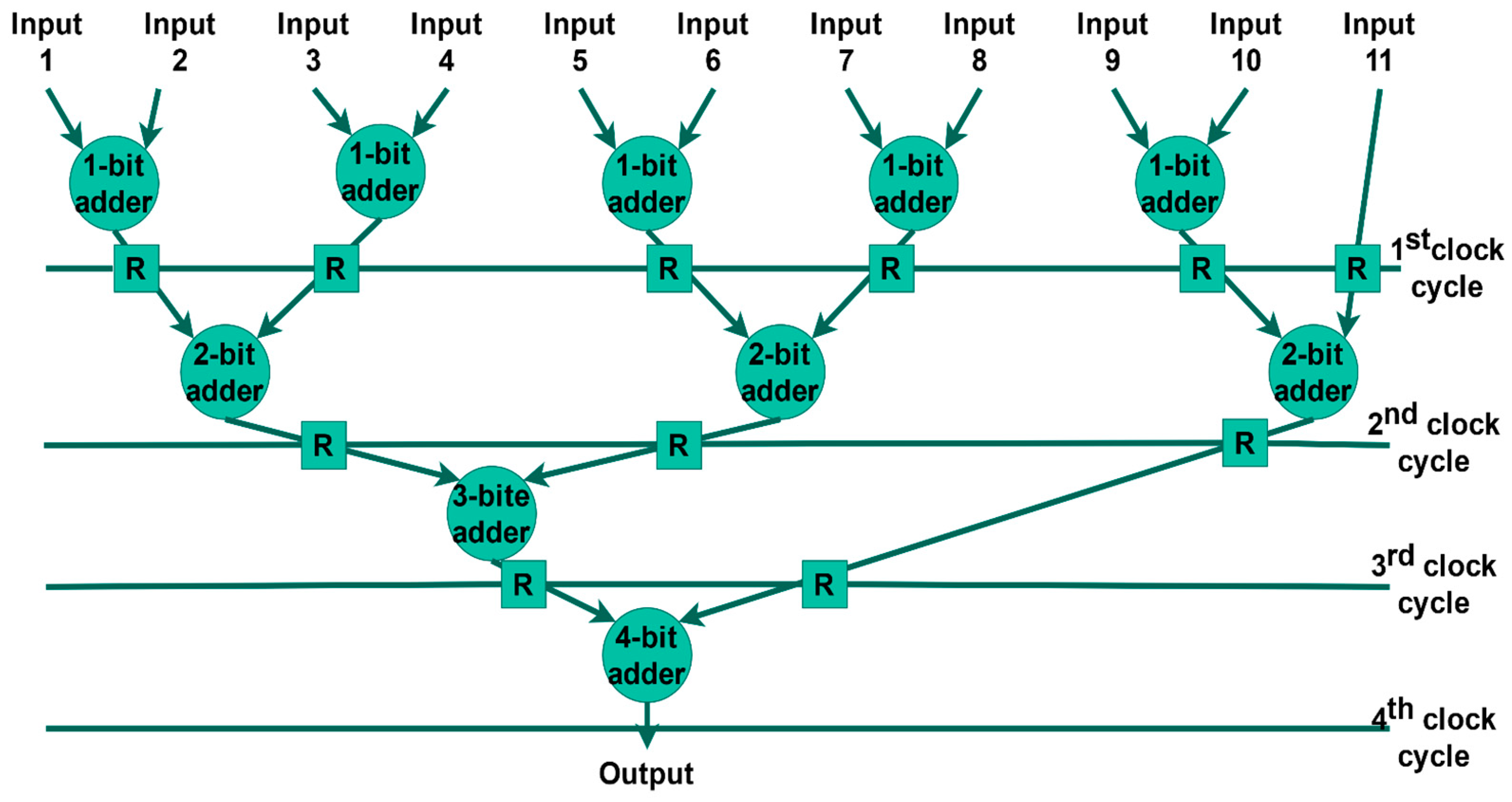
2.1. Adder Tree
2.2. Comparator Tree
3. Core Circuit Description
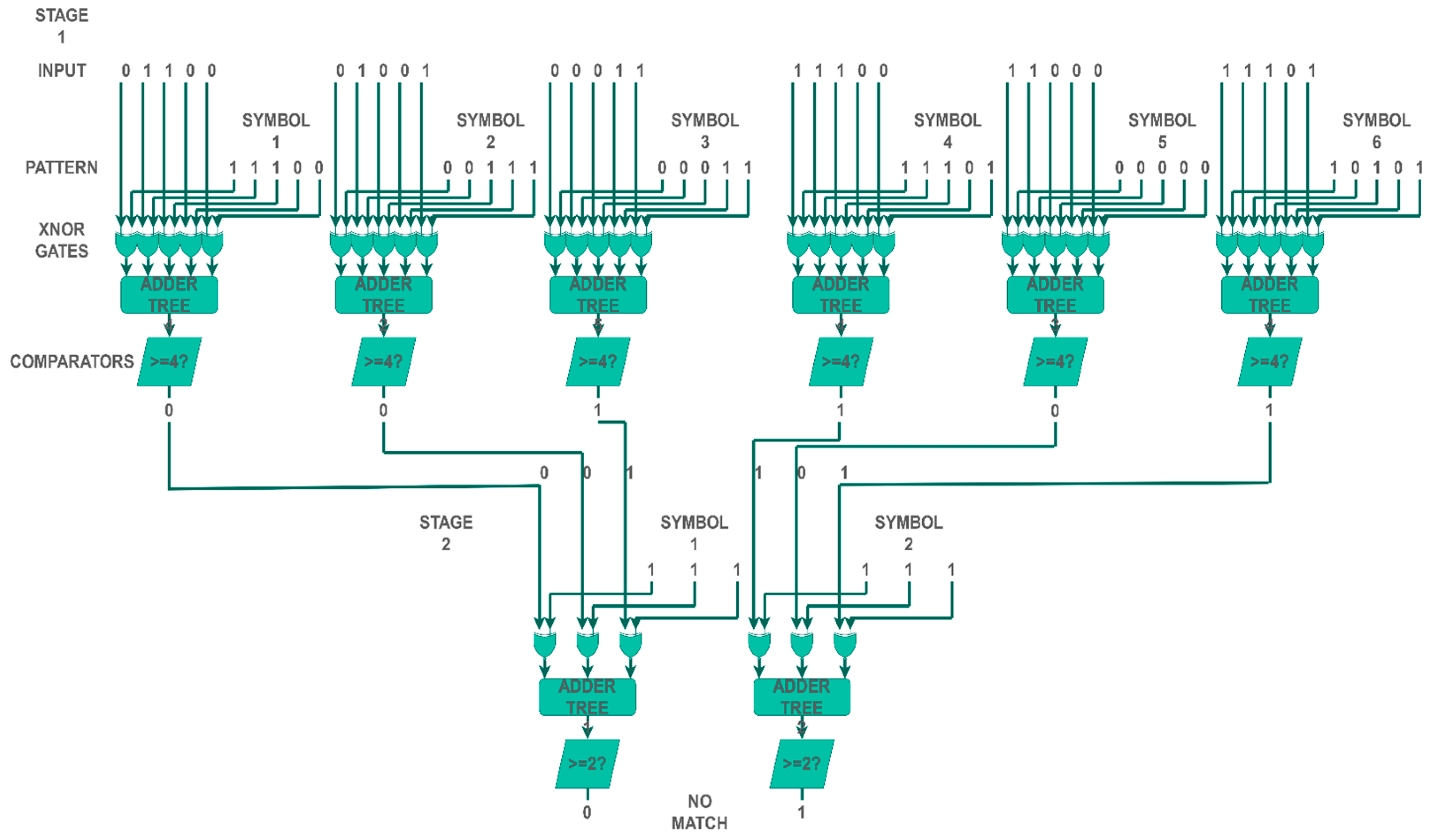
3.1. Lesser Pattern Identifier
3.2. Cascaded Pattern Identifier
4. Pattern-Matching Circuit and Implementation
5. Pattern Matching under Interference and Simulations
5.1. Error-Free and Error-Present Input Generation
5.2. Error-Free and Error-Present Simulations
6. Summary
Author Contributions
Funding
Data Availability Statement
Conflicts of Interest
References
- Pong, F.; Tzeng, N.F. HaRP: Rapid Packet Classification via Hashing Round-Down Prefixes. IEEE Trans. Parallel Distrib. Syst. 2011, 22, 1105–1119. [Google Scholar] [CrossRef]
- Cho, Y.H.; Mangione-Smith, W.H. Deep network packet filter design for reconfigurable devices. ACM Trans. Embed. Comput. Syst. 2008, 7, 26. [Google Scholar] [CrossRef]
- Thinh, T.N.; Hieu, T.T.; Kittitornkun, S. A FPGA-based deep packet inspection engine for Network Intrusion Detection System. In Proceedings of the 2012 9th International Conference on Electrical Engineering/Electronics, Computer, Telecommunications and Information Technology, Phetchaburi, Thailand, 16–18 May 2012; pp. 1–4. [Google Scholar] [CrossRef]
- Le, H.; Prasanna, V.K. A Memory-Efficient and Modular Approach for Large-Scale String Pattern Matching. IEEE Trans. Comput. 2013, 62, 844–857. [Google Scholar] [CrossRef]
- Dlugosch, P.; Brown, D.; Glendenning, P.; Leventhal, M.; Noyes, H. An Efficient and Scalable Semiconductor Architecture for Parallel Automata Processing. IEEE Trans. Parallel Distrib. Syst. 2014, 25, 3088–3098. [Google Scholar] [CrossRef]
- Alyushin, A.V.; Alyushin, S.A.; Arkhangelsky, V.G. Scalable processor core for high-speed pattern matching architecture on FPGA. In Proceedings of the 2016 Third International Conference on Digital Information Processing, Data Mining, and Wireless Communications (DIPDMWC), Moscow, Russia, 6–8 July 2016; pp. 148–153. [Google Scholar] [CrossRef]
- Qu, Y.R.; Zhou, S.; Prasanna, V.K. High-performance architecture for dynamically updatable packet classification on FPGA. In Proceedings of the Ninth ACM/IEEE Symposium on Architectures for Networking and Communications Systems, San Jose, CA, USA; 2013; pp. 125–136. [Google Scholar] [CrossRef]
- Thomas, M.V.; Kanagasabapthi, C.; Yellampalli, S.S. VHDL implementation of pattern based template matching in satellite images. In Proceedings of the 2017 International Conference on Smart Technologies for Smart Nation (SmartTechCon), Bengaluru, India, 17–19 August 2017; pp. 820–824. [Google Scholar] [CrossRef]
- Xilinx. Virtex-6 LXT FPGA Product Table. Available online: https://www.xilinx.com/publications/prod_mktg/Virtex6LXT_Product_Table.pdf (accessed on 15 December 2022).
- Gilbert, E.N. Capacity of a burst-noise channel. Bell Syst. Tech. J. 1960, 39, 1253–1265. [Google Scholar] [CrossRef]
- Kim, T.; Lee, H.; Koh, J.; Lhee, K. A performance analysis of polling schemes for IEEE 802.11 MAC over the Gilbert–Elliot channel. AEU Int. J. Electron. Commun. 2009, 63, 321–325. [Google Scholar] [CrossRef]
- Yang, Z.; Li, H.; Jiao, J.; Zhang, Q.; Wang, R. CFDP-based two-hop relaying protocol over weather-dependent Ka-band space channel. IEEE Trans. Aerosp. Electron. Syst. 2015, 51, 1357–1374. [Google Scholar] [CrossRef]


| Input Pattern | 0011011101 |
|---|---|
| Rule 1 | 1101001101 |
| Rule 2 | 0001011101 |
| Rule 3 | 1001011111 |
| Rule 4 | 1111110101 |
| Rule 5 | 1011110100 |
| Input Pattern | Rule 2 | Xnor | Sum of Xnor Gates |
|---|---|---|---|
| 0 | 0 | 1 | 9(1001) |
| 0 | 0 | 1 | |
| 1 | 0 | 0 | |
| 1 | 1 | 1 | |
| 0 | 0 | 1 | |
| 1 | 1 | 1 | |
| 1 | 1 | 1 | |
| 1 | 1 | 1 | |
| 0 | 0 | 1 | |
| 1 | 1 | 1 |
| Source | Hardware | Terminal Throughput |
|---|---|---|
| [7] | 116,224 LUTs/232,448 FFs | 256 Gbps |
| [6] | N/A | 358.4 Gbps 1 |
| [2,3,4] | Various (not specialized) | <30 Gbps |
| Proposed | 205,082 LUTs/355, 013 FFs | 800.4 Gbps |
Disclaimer/Publisher’s Note: The statements, opinions and data contained in all publications are solely those of the individual author(s) and contributor(s) and not of MDPI and/or the editor(s). MDPI and/or the editor(s) disclaim responsibility for any injury to people or property resulting from any ideas, methods, instructions or products referred to in the content. |
© 2023 by the authors. Licensee MDPI, Basel, Switzerland. This article is an open access article distributed under the terms and conditions of the Creative Commons Attribution (CC BY) license (https://creativecommons.org/licenses/by/4.0/).
Share and Cite
Nikolaidis, D.; Groumas, P.; Kouloumentas, C.; Avramopoulos, H. High-Throughput Bit-Pattern Matching under Heavy Interference on FPGA. Electronics 2023, 12, 803. https://doi.org/10.3390/electronics12040803
Nikolaidis D, Groumas P, Kouloumentas C, Avramopoulos H. High-Throughput Bit-Pattern Matching under Heavy Interference on FPGA. Electronics. 2023; 12(4):803. https://doi.org/10.3390/electronics12040803
Chicago/Turabian StyleNikolaidis, Dimitris, Panos Groumas, Christos Kouloumentas, and Hercules Avramopoulos. 2023. "High-Throughput Bit-Pattern Matching under Heavy Interference on FPGA" Electronics 12, no. 4: 803. https://doi.org/10.3390/electronics12040803
APA StyleNikolaidis, D., Groumas, P., Kouloumentas, C., & Avramopoulos, H. (2023). High-Throughput Bit-Pattern Matching under Heavy Interference on FPGA. Electronics, 12(4), 803. https://doi.org/10.3390/electronics12040803