Article

Impact of the Noise on the Emulated Grid Voltage Signal in Hardware-in-the-Loop Used in Power Converters

1
Escuela Superior de Ingeniería y Tecnología, Universidad Internacional de La Rioja, 26006 Logroño, Spain
2
Departamento de Ingeniería Informática y Electrónica, Universidad de Cantabria, Avd. Los Castros s/n, 39005 Santander, Spain
3
Departamento de Tecnología Electrónica, Ingeniería de Sistemas y Automática, Universidad de Cantabria, 39005 Santander, Spain
*
Author to whom correspondence should be addressed.
Electronics 2023, 12(4), 787; https://doi.org/10.3390/electronics12040787
Submission received: 30 December 2022 / Revised: 20 January 2023 / Accepted: 31 January 2023 / Published: 4 February 2023
(This article belongs to the Special Issue Hardware in the Loop and Real-Time Simulation)

Abstract

:
This work evaluates the impact of the input voltage noise on a Hardware-In-the-Loop (HIL) system used in the emulation of power converters. A poor signal-to-noise ratio (SNR) can compromise the accuracy and precision of the model, and even make certain techniques for building mathematical models unfeasible. The case study presents the noise effects on a digitally controlled totem-pole converter emulated with a low-cost HIL system using an FPGA. The effects on the model outputs, and the cost and influence of different hardware implementations, are evaluated. The noise of the input signals may limit the benefits of increasing the resolution of the model.

1. Introduction

Hardware-in-the-Loop (HIL) is used to emulate physical systems with programmable/reconfigurable digital devices in real time. This allows testing diverse operational conditions, allowing the verification of the controllers and any further analysis before interacting with the real system [1].
In the context of power converters, a HIL uses mathematical models to emulate the behavior of the real power converter stimulated with control and power signals, so that the controller measures a set of HIL variables and, from that, obtains the required control signals. During the HIL-based test, the controller receives measurements of the observable variables from the HIL and sends the required control signals to operate the HIL in real time. This technique is often used to validate controllers for power converters quickly, repetitively, flexibly, cheaply, and safely [2]. In addition, it provides information for the optimization of the real hardware after testing the behavior of the converter in a wide range of input and output conditions, including faults, such as power outages or drive component failures.
Due to the potential of HIL, many studies have been presented proposing to test the behavior of control algorithms [3]; distributed energy systems such as microgrids [4] and solar energy systems [5]; high energy efficiency, low-voltage power systems, such as LED power supplies [6]; and battery storage [7]; etc. Studies of available technology have detected associated problems and sources of errors with the development of models in emerging applications, and they have been delved into.For example, different mathematical methods have been proposed for modeling power converters, such as the Euler method, which is popular for its simplicity and reduction of latencies, and more advanced ones, such as Runge-Kutta, which under the conditions in [8] results in the most accurate model. Some HIL converter topologies connected to the grid present errors in the zero crossings of the emulated signals, with two main proposals to solve this problem: (i) forcing the mathematical model through code so that the signal takes the appropriate values, or (ii) performing a subdivision of integration steps from linear approximations around the operating point [9]. This last proposal is not accidental. The choice of the integration step has a significant impact on the accuracy and error of the HIL [10]. Another widely studied parameter is the data-type format of the system variables [11]. This becomes especially relevant when modeling the system losses, since they increase the complexity of the system and are not essential in all models [12]. Also, the resolution of the duty cycle may be limited by the clock frequency of the HIL and other application-related limitations [10]. The sources of error are very diverse, such as failures in reading the input data to the system [13], inaccuracy of the model due to the chosen mathematical model [8], or poor choice of the integration step [14]. However, their influence varies according to the type of system to be modeled and the objective for which it is modeled.
It has been observed that recent publications on HIL in power electronics often assume that power converters work with an ideal signal to emulate the input voltage, without considering the input signal noise effects on the HIL and how it may deteriorate the system emulation. Recent literature neglects the noise effects on input signals. To address this gap in knowledge, this manuscript proposes to thoroughly evaluate the impact of emulated grid voltage on the HIL, explicitly focusing on the noise that enters through the analog-to-digital converter (ADC). To meet this objective, the first section of this work reviews the main sources of error that can affect HIL results, and introduce the noise-related problems, the techniques available to mitigate them, and how to measure them. Section 3 presents a case study to illustrate the effect of noise on the input signals in a totem-pole converter. The case study will include the design and implementation of a low-cost HIL using two Field-Programmable Gate Arrays (FPGAs) to emulate the behavior of a digitally controlled totem-pole converter. Finally, the conclusions are presented.

2. Error Source Affecting a HIL

A source of error refers to any factor, controlled or not, that can contribute to imprecise or inaccurate results of a measurement or experiment [15,16]. Its importance and impact on the system depend on the power converter, mathematical model, and implementation method. The knowledge of sources of errors [17,18] enables the developer to take preventive measures that minimize or eliminate the effects of such errors, making the emulation more accurate and verifying that the results match the specifications.
The sources of error in a model of a power converter used in HIL can be summarized as follows:
  • Errors in the implementation of the model [19,20], such as the omission of specific physical effects in the model, such as losses, or the oversimplification of some aspects of the system [21], errors in the mathematical formulation of the model, or errors due to the chosen numerical format. Omitting certain physical effects can also affect accuracy. For example, if the model does not account for electrical resistance in a circuit, it can produce inaccurate results for the voltage drop in the circuit. On the other hand, errors in the mathematical formulation of the model may include errors in the definition of the equations or constants, which are used to describe the behavior of the system or mistakes in the implementation of these equations in the code.
  • Errors measuring the input and output signals of the model [22], such as calibration, data acquisition, or sampling errors. If a poorly calibrated sensor is used to measure an input signal, it can produce an inaccurate input signal that affects model accuracy. Whereas, in the case of data acquisition, if a low sampling rate is used to capture all the variations in a signal, it can result in an inaccurate input or output signal affecting the accuracy of the model [23].
  • Errors in the execution time [24,25]. These errors refer to the difference between the expected time to execute a task and the actual time expected to complete that task due to processing speed or workload issues.
  • Synchronization errors [26]. The latency between the model and the hardware can cause timing, communication, and test accuracy errors.
  • Uncontrolled external conditions [27,28]. The model may not account for all external variables, such as electromagnetic interferences [29], that can affect the behavior of the actual system, which can introduce errors in the predictions of the model.
  • Inaccurate or noisy input data [30]. Noise in an electrical signal is defined as an unwanted disturbance deviating from the signal, typically random. Its origins are diverse, but can be classified into noise inherent to the system and external noise, in this case, AC-input noise. The total inherent noise in an ADC is mainly due to uncorrelated quantization and thermal noises. Quantization noise is due to mapping the input signal to a finite set of digital codes, and oscillates at a known threshold, depending on two fundamental factors: the number of bits in the ADC and the input signal range. On the other hand, thermal noise is inherent in all electrical components because of the temperature effects on the physical movement of electrical charges. It is dependent on the ADC design and manufacturing processes. It typically exhibits a Gaussian distribution in the time domain, and it is broadband. The user cannot modify the ADC thermal noise. Furthermore, the predominance of one type of noise or another in the ADC depends on its resolution; thus, in a low-resolution ADC, quantization errors will predominate, while in a high-resolution ADC, thermal noise will predominate. In this sense, the ADC is not trivial [31,32]. Different types of ADC can be used in building a HIL. Although all of them can be affected by noise due to random jitter in the signal during digital conversion, each is affected by other types of noise based on its characteristics. So, for example, successive approximation register (SAR) ADCs tend to be more prone to sampling noise, and counter ADCs tend to be more prone to counter noise, while sigma-delta ADCs avoid these errors by using a modulation technique that allows high-frequency noise to be removed.
In general, it is important to be aware of these sources of error and try to minimize them to obtain accurate results.

2.1. Noise in the Input Data Effects

If noise is present in the external signals of a model, a HIL-emulated power converter can exhibit different issues depending on its severity, such as:
  • Signal distortion: Including noise in the signal can distort the latter, making it deviate from the ideal signal.
  • Difficulty in interpreting the signal: The level of noise present can make it challenging to analyze the signal and obtain information from it, especially around zero values or in quasi-stationary conditions.
  • Reduction of the signal to noise: If the noise signal is excessively high, the signal can be reduced to noise only, and practically useless for the system.
  • Loss of information: Noise can hide valuable information in the signal. This unwanted phenomenon can negatively affect the precision, stability, and even processing time of the model used.
Signal-to-noise ratio (SNR) of the signals input to the HIL is combined with the SNR of their digital conversion. A noisy input signal reduces the equivalent number of bits (ENOB). This can harm the model, making it less stable and even more prone to unpredictable behavior and/or crashes. A simple example of this phenomenon can occur in systems with negative feedback [33]. If the model overresponds to minor variations in the input data, the model outputs are erroneous. If, in turn, these are used to provide feedback on the model, they can cause the result to change again and enter a lousy data loop. In this situation, the model can become unstable and lose its ability to predict accurately.
In the implemented model, noise can affect the processing time and the consumption of necessary hardware resources due to the need to filter the noise to mitigate or eliminate it and/or use other strategies that achieve the same result [34], such as oversampling the input data. Implementing these strategies can slow down the system’s performance and/or increase operating costs.
On the other hand, this abnormal behavior can affect the digital controls to be tested with the HIL technique, which will not receive the expected information [35]. Consequently, its real behavior cannot be guaranteed. Such is the case of digital controls based on predictive models or machine learning [36]. In these, the model is trained with the input and output data from the HIL to improve accuracy, and may be compromised by signal noise.
Given the above, the minimization of noise in the input signals can be guaranteed by the precision and accuracy of the mathematical model. However, noise can be used to evaluate the emulated system. It is possible to add a noise signal to the input of the converter to assess how the HIL system responds to such noise and whether it can distinguish between valid input signals and the noise. In these cases, it is considered that the noise indirectly affects the mathematical model of the converter because it is used as a stimulus of the devised HIL system.

2.2. Measurement of the Noise Introduced in the Input Signals

Just as designers and engineers use different devices to build their HIL models, depending on the application and system needs, there are different methodologies for measuring the noise of HIL input signals:
  • Noise sensors and/or meters [37]: These components or pieces of equipment measure the noise in the input signal of the HIL system.
  • Signal processing techniques: These techniques are a set of algorithms and methods used to improve the quality and accuracy of input signals by removing unwanted noise or interference. Examples of these techniques are Fourier analysis [38] and wavelet transform [39].
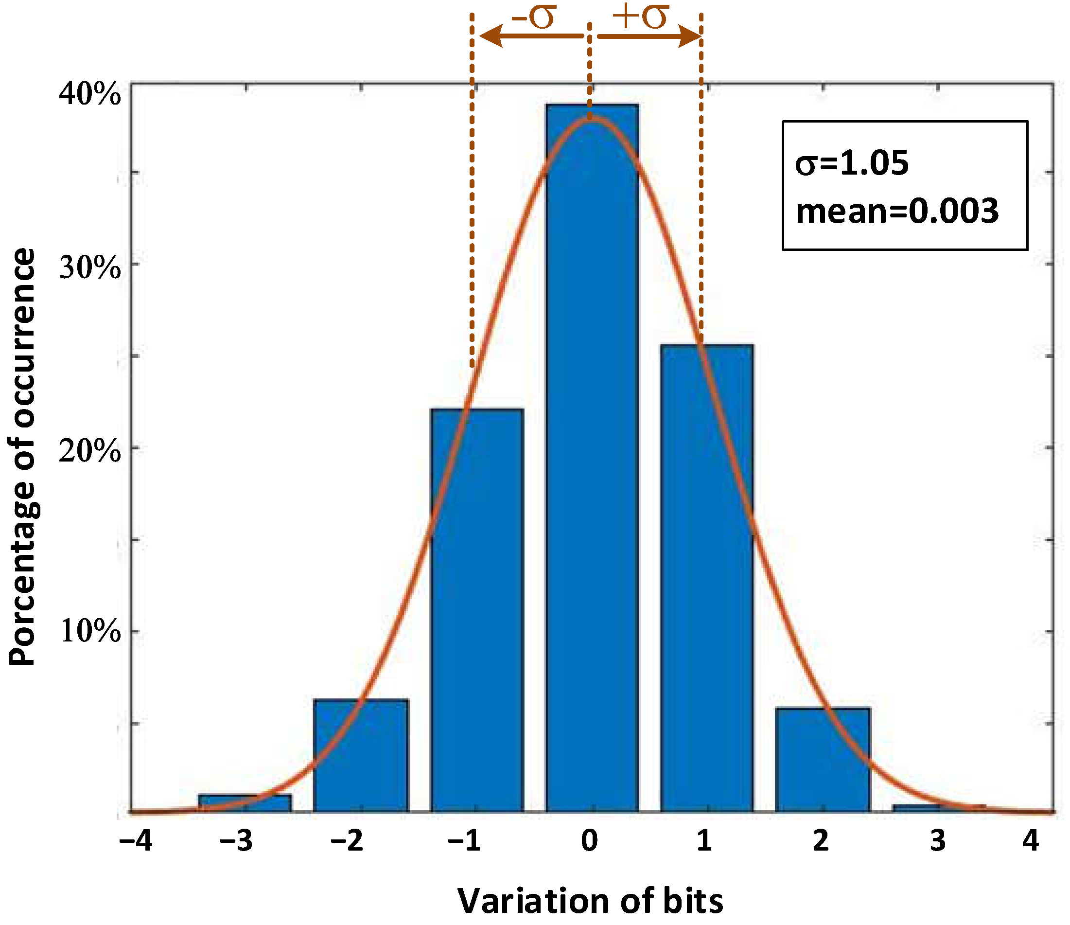
  • Sinewave-input and DC-input tests: The sinewave-input test assesses the performance of the ADC when faced with a known sinusoidal signal of a certain amplitude and frequency, in order to evaluate the manner in which the ADC converts the signal. The DC-input test measures the DC noise of the signal by using histograms [40,41], which are graphs that show the probability density function (PDF). Noise level measurements are acquired over a specific period. They are grouped in intervals and displayed in a bar graph to show the number of measurements falling within a specific range of noise levels, and to detect abnormal noise levels or patterns in the noise distribution. The histogram shows whether most of the noise is allocated in a specific frequency range, or distributed more uniformly throughout the intervals.
The key noise sources in the ADC are quantization, wideband noise (generally referred to as input-referred noise), and noise. Wideband ADC noise produces a certain amount of RMS noise, which is characterized by examining the histogram generated after applying a large number of samples [40]. In wideband SAR or sigma-delta ADCs, this parameter is critical. The noise is characterized by the Signal-to-Noise Ratio and Distortion (SINAD). The SINAD computes the ratio of the RMS level of the input signal to the RMS value of the root-sum-square of all noise, distortion, and harmonics components in a fast Fourier Transform (FFT) analysis (excluding the DC components). From the SINAD the Effective Number of Bits (ENOB) within the frequency band is derived assuming constant noise energy distribution over frequency,.
Factors to consider when choosing the appropriate measurement systems are the purpose of the measurement, the type of noise to be measured, its time dependence, the cost and complexity of the measurement, and how it interferes with the system. Otherwise, models and operation scenarios defined in simulation tools, such as Matlab, LabView [42], LTSpice [43], or PLECS [44], are used to predict the noise level in the input signal of the HIL.

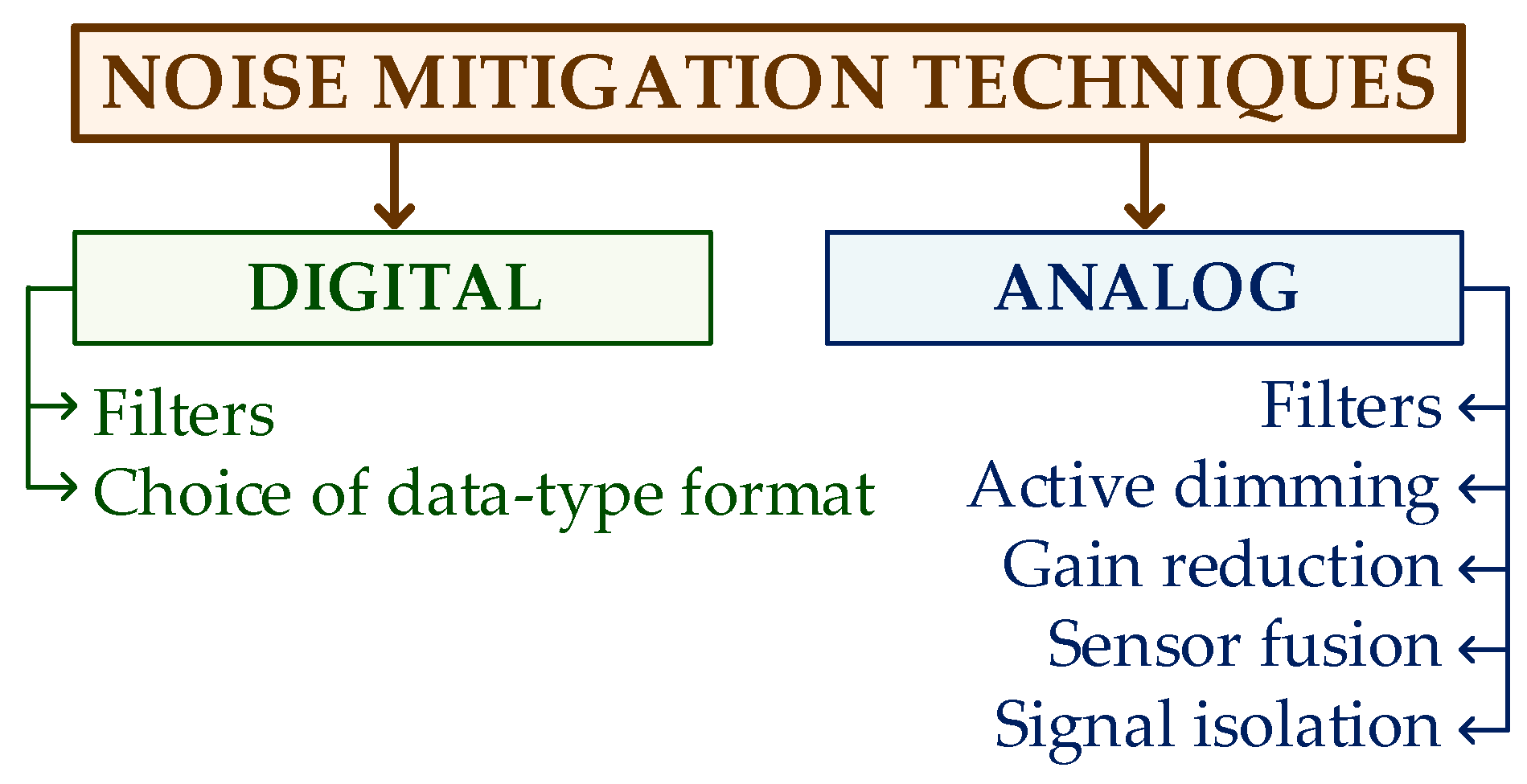
2.3. Noise Mitigation Techniques

Various techniques can be used to remove or mitigate noise in an input signal, depending on the type of noise, its measured level, and the application. In general, these techniques can be classified into analog and digital, depending on the type of signals on which they act (Figure 1).
  • Filters [45]: Filters are circuits or algorithms that allow noise to be removed or attenuated from an input signal. The type of filter, moving average [46], interpolation [47], or downsampling, is selected upon the characteristics of the noise, the frequency of the input signal, and the disturbance.
  • Choice of model data-type format [13]: Data-type format refers to how numbers are represented in a system. Although its design affects accuracy and therefore noise, it does not necessarily reduce it. However, it enables the definition of the system’s precision and simultaneously sets a range of allowed values. A good design reduces the rounding and truncation effects.
  • Active dimming [48,49]: This technique uses active components, such as op-amps or specific integrated circuits, to perform dimming. This achieves higher flexibility and precision in the attenuation of the signal since the parameters can be adjusted dynamically.
  • Gain reduction [50]: The gain reduction technique decreases the amplification of the input signal to reduce signal noise.
  • Sensor fusion [51]: This process combines data from several sensors to obtain a more accurate and complete representation of a specific variable or condition. The sensors do not need to be the same.
  • Signal isolation: Signal isolation consists of isolating the input signal from external noise using techniques such as galvanic isolation or electrical isolation.
The analog-to-digital, digital-to-analog, and digital-to-digital interfaces used with power-hardware-in-the-loop (PHIL) are also prone to suffer issues related to noise. In PHIL, the performance of the equipment under test (EUT) is evaluated with very different operation conditions, at both the input and the output sides, emulated through dedicated power interfaces. PHIL tests benefit from the noise-control techniques shown in Figure 1 used with signals from/to the controller and power interfaces. In [52], multirate discrete modeling is proposed and compared with other traditional techniques, while in [53], a new interface of an advanced ideal transformer model, which improves the stability of the system, is proposed.

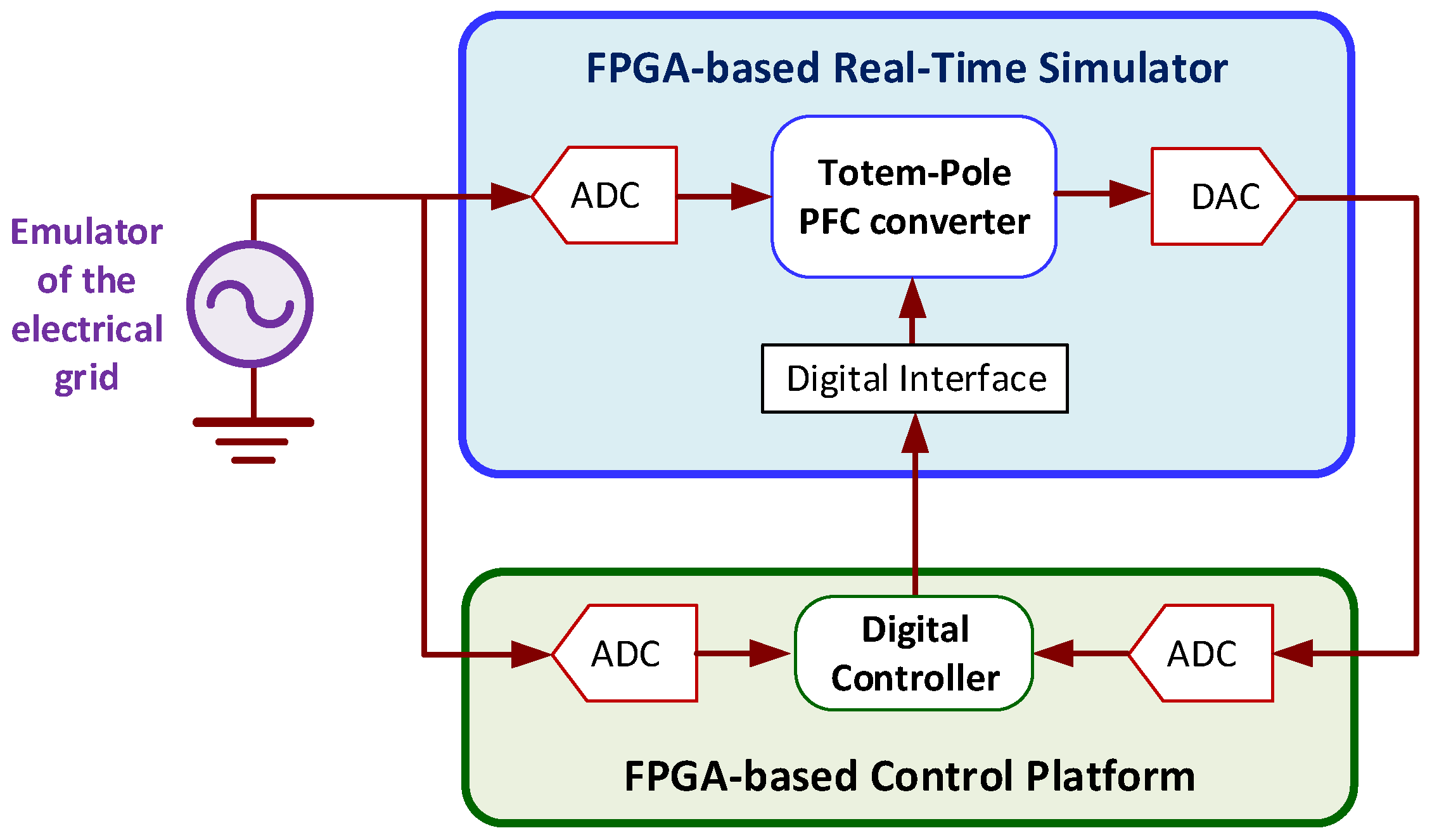
3. Case Study of Noise Implications

A totem-pole converter with linear control of current and voltage described in [54] is implemented in a Field Programmable Gate Array (FPGA) type device to be tested. Figure 2 shows the schematic diagram of the tested system, which is synthesized with two Xilinx® 7 series FPGA (XC7A100T-1CSG324C) platforms operating at 100 MHz, which include SoC XADC with on-chip sensor (dual 12-bit (N), 1 MSPS, 1 V Full Scale (VFS), SAR-type), 240 DSP slices and 4.3 Mb RAM. The data exchange is carried out in two ways: through an analog interface based on ADC and DAC that generates signals corresponding to simulated voltages, and with a direct digital interface. Additional ADCs are used to input external emulated signals such as the grid voltage.

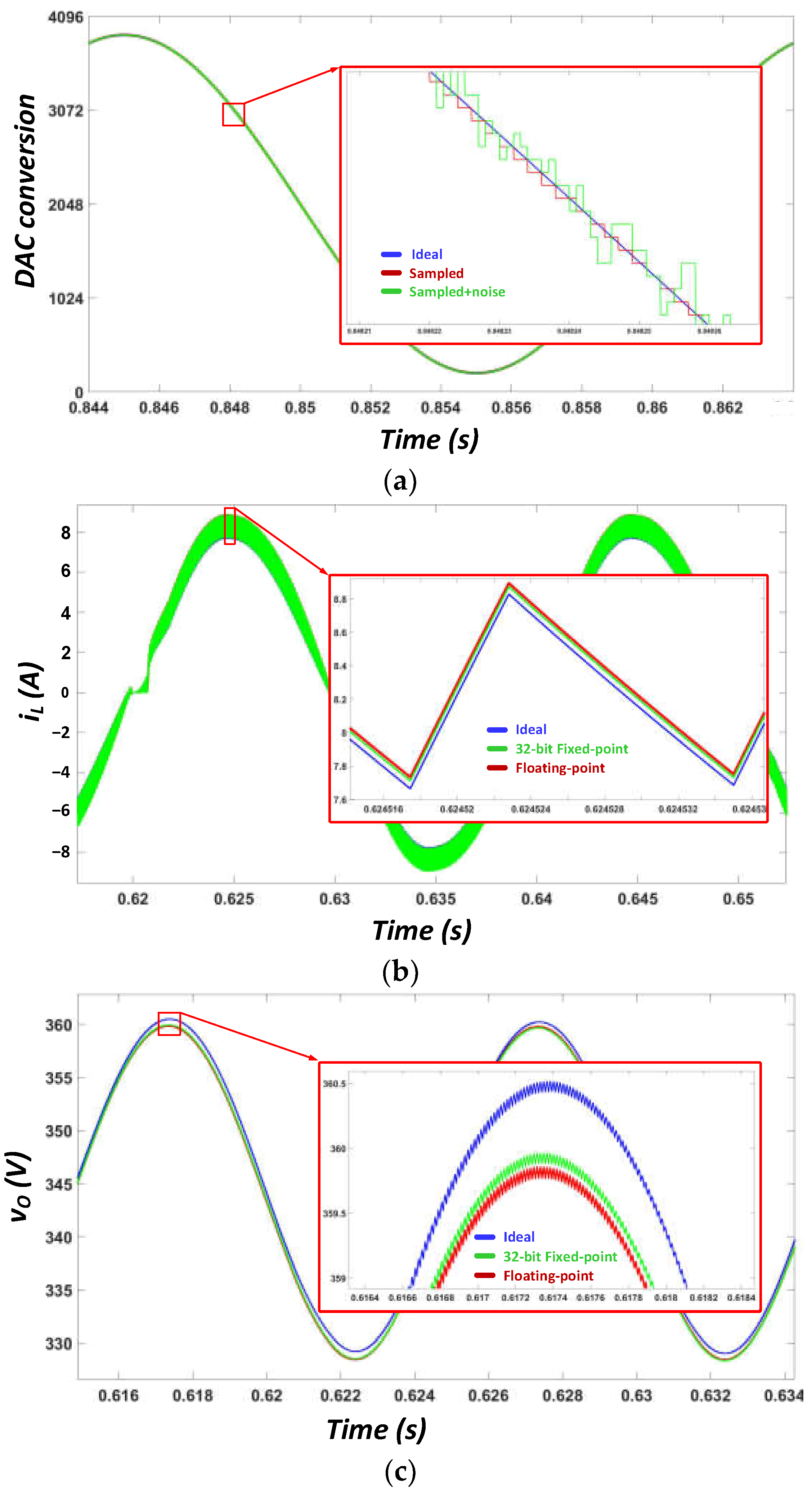
3.1. Characterization of the ADC Noise

In this case study, the noise of the SoC XADC using experimental measures including external noises is characterized.
N-bit ADC with an analog full-scale input range, VFS, presents a corresponding least significant bit (LSB) step size or resolution, i.e., bin, of
V L S B = V F S 2 N 1 .
Applying this equation to the XADC, VFS = 1 V, N = 12 bits, so its resolution is VLSB = 244.2 μV. The ideal quantization error is uniformly distributed [55] and the standard distribution, σQ, is given by
σ Q = V L S B 12 .
In this case, σQ = 70.5 μV.
Figure 3 shows the results obtained by applying 218 samples to the XADC of the FPGA using a DC-input of 0.5 V. Since the noise histogram has a Gaussian distribution, the definition of noise performance is typically one standard deviation. Therefore, as highlighted in Figure 3, the wideband noise for this XADC is σWB = 1.05 bits (256.4 μV).
Figure 4 shows the FFT of the XADC’s output noise measured for an input sine wave with an amplitude of 0.45 V and 50 Hz frequency. This plot highlights the fundamental component, harmonics components, and background noise. The experimental value of the SINAD for this XADC is 60.17 dB.
In this XADC, the ENOB is given by
E N O B = S I N A D 1.76 + 20 log 10 V F S 2 V I 6.02 = 9.85 b i t s ,
where the input amplitude of the signal, VI, is 0.45 V. The ENOB is derived from SINAD and is not meant to convey wideband performance. In this case, the noise is σD = NENOB = 2.15 bits (525 μV), which is more restrictive than the wideband noise. However, some authors recommend using the wideband noise for ADC noise analysis [32].
Therefore, the total noise presents a standard deviation, σT, given by
σ T = σ Q 2 + σ D 2 = 529.7   μ V .
Considering σT, an equivalent statistical representation in Figure 5 models the XADC. Here, the input signal, x(t), is sampled at a frequency, fs (1 MHz) and the noise, e(n), is an uncorrelated random Gaussian distribution variable with a standard deviation σT = 529.7 μV. Indeed, the amplitude of the emulated grid voltage including the noise can be expressed as Vg = 230√2 ± 0.38 V.
Assuming a sinusoidal input signal, the SNR
S N R = 20 log 10 x r m s σ T
depends on its amplitude. To reach the maximum SNR, the amplitude should be VFS/2, which is unfeasible due to clipping effects. In this example, the sine wave of 0.45 V amplitude is applied to the input of this XADC, and then the SNR = 55.57 dB (xrms = 0.45/√2 V).
In linear shift-invariant systems, the response to x(n) and e(n) are separately computed, and the variance of the output noise, σO, is expressed as
σ o 2 = σ T 2 n = h n 2 ,
where h(n) is the impulse response of the ideal converter, and no other noises were considered [55].

3.2. Relevance of the Model Data-Type Format

The arithmetic used in the realization of the FPGA-based systems introduces additional noise and its effects superimposed to the noise of the signal [56]. The fixed-point arithmetic presents truncation and round-off error which is modeled as a Gaussian noise with a variance of
σ f i x 2 = 2 2 F 12 ,
where F is the number of bits of the fractional part. In contrast, floating-point arithmetic involves relative errors with a theoretical variance of
σ f l o a t 2 = 2 2 B 6 0.167 2 2 B ,
according to [57], where B is the number of bits of mantissa.
The comparison of both standard deviations proves that floating-point has roughly 3000 times less dynamic quantization noise than fixed-point [57]. However, the floating point presents a higher static range of noise, which is dominant in some applications.
Analytical calculation of the effect of these noises at the output uses Equation (6). Floating-point arithmetic introduces less noise, and it allows translating equations from the mathematical model to code in a more straightforward way. Moreover, the programmers do not generally need to handle overflow, underflow, and round-off errors [58]. However, with limited resources in FGPA-based implementations, special attention must be paid to the occupied area, the speed and the integration step [42]. Therefore, the fixed-point arithmetic allows higher switching frequency with a lower occupied area when a tiny integration step is sought. Different approaches, like [56,59,60], have been proposed to find a good trade-off between accuracy and resources by using methods that reduce this effort design to a minimum.

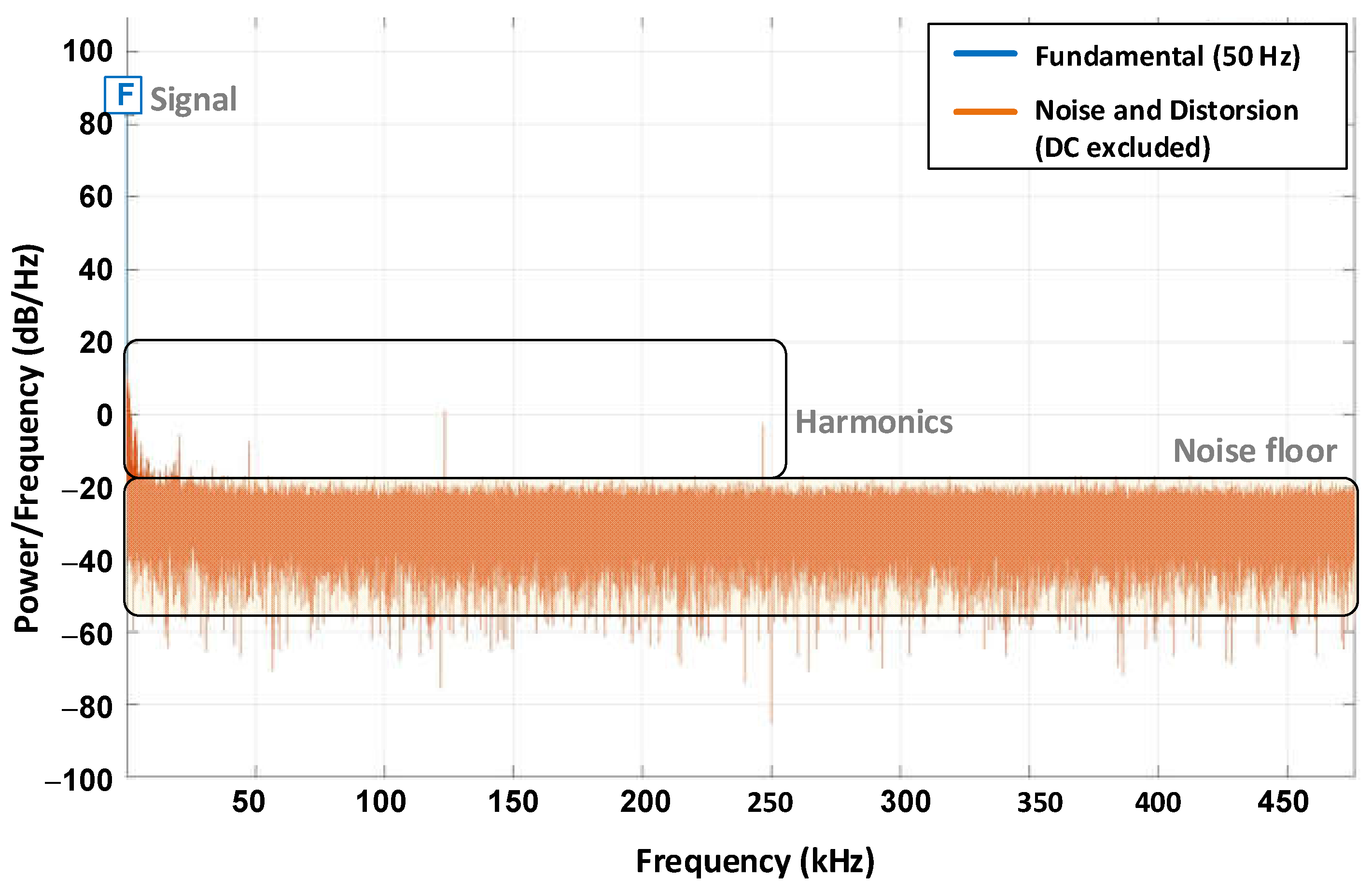
3.3. Effects of Noise on the Mathematical Model and the Hardware Implementation

In this practical case, the simulation of the HIL was performed by the Xilinx Vitis High-Level Synthesis (HLS) platform, which allows creating of complex FPGA-based algorithms using C/C++ code. It supports fixed-point numbers with different word lengths and floating-point numbers with the IEEE-754 32-bit single precision format consisting of a 1-bit sign, 8-bit exponent, and 23-bit mantissa. The integration time step is set to 50 ns. Figure 4 shows the waveform of the input and output signals of the model. The summary of simulation and synthesis results using different data types and word length is shown in Table 1.
The simulation of the totem-pole converter in a double-precision floating-point data type to only analyze the effect of the ADC noise in the input to the HIL signal that represents the grid voltage (Figure 6a) provides a standard deviation of 7.9 mA for the inductor current, iL, and 106.3 mV for the output voltage, v0, (Figure 6b,c). The 32-bit fixed-point arithmetic provides fewer σ (8 mA for iL, 106.9 mV for v0) than the floating-point one (28.2 mA, for iL, 194.1 mV). In order to reduce the round-off error in the fixed-point multiplications, a rounding approach, instead of truncation, has been used. The round-off error is sensitive to the specific value of the multiplier coefficient, the dynamic range of the signal, and the bandwidth of the signal [61].
According to the simulation results, the major noise source is obtained in the 32-bit fixed-point data type comes from ADC. With 28 bits, a similar standard deviation is attained with a minor reduction in hardware resources. However, the 24-bit implementation significantly reduces hardware resources by increasing the deviation of iL. This allows some leeway for the designer to adjust the word length of the fixed-point arithmetic and maintain noise levels low. In the hardware implementation of the totem pole, floating-point consumes more resources (in terms of DSP, FF, and LUT) with a latency of 2 more cycles compared to the fixed-point implementations.

4. Discussion

The effects of the input signal noise limit the accuracy of the model of a converter used in HIL. From the case study presented, it can be seen that this noise can lead to a standard deviation of the error that is tens of milliamps in the output current (in an ideal 8 A signal) and tenths of a volt in the case of the output voltage signals of the converter (when the maximum values are around 360 V). The designer defines a precision of the model signals that results in a theoretical SNR 10 dB higher than the SNR of the input signal, to not reduce the SNR.
On the other hand, the study of the model behavior under different data-type formats has shown that the proper choice of the resolution bin diminishes the effects of input noise and simultaneously optimizing the hardware resources used. In addition, these results are consistent with those obtained in other works, such as in [62].
Although it is applied in a low-cost system, the methodology described in this case study can be used to evaluate the ADCs of any device used to configure a HIL system. In the case of commercial hardware, such as OPAL-RT products, it is necessary to analyze case-by-case. Thus, the low-cost, powerful entry-level simulator OP4512 includes 16 ADCs (16-bits, 1 MSPS, and ±20 V). While the OP5707XG model (more powerful than the previous one) also includes 16 ADCs, but its characteristics are 16-bit, 2 MSPS, and ±20 V. With these characteristics, it is expected that the dominant ADC inherent noise is due to the thermal noise, and noise due to quantization is lower than that obtained in this case study due to the higher number of bits and the full-scale input voltage available. Regarding external noise, the OPAL-RT products allow configuring the model to include a grid emulator with the desired characteristics together with the mathematical model of the converter, thus eliminating the appearance of unwanted external noise in the input signal and testing on ideal conditions.

5. Conclusions

The objective of HIL circuits is to evaluate the performance and reliability of power electronic converter controllers under realistic operating conditions without building a complete prototype. The precision and reliability of the results are affected by the input signals’ noise. In this manuscript, an in-depth review of the main sources of error has been made. The knowledge of these enables the designer to implement measures to minimize their impact, optimizing the design in terms of resolution and computational cost.
A common source of error in this system is noise in the input signals of the HIL systems used for emulation of power converters. To minimize the noise, designers have at their disposal diverse filter tools. Later, analysis and simulation tools based on the noise characteristics tools help to define the requirements of their system. These techniques, and how to measure the noise in the input, have been reviewed in this manuscript.
To illustrate the influence of input noise in a HIL system, a case study of the effect of noise in a totem-pole converter, digitally controlled by a linear voltage and current control in low-cost HIL, using low-cost FPGAs, is presented. The results show that fixed-point arithmetic in FPGA-based HILs is the best option for optimizing the required hardware resources according to the error in the input signals.
Overall, this manuscript has emphasized the need for further research of noise effects in HIL systems to improve the accuracy and effectiveness of the emulated power converters. The study presented in this manuscript serves as an example of how to evaluate the impact of noise on input signals in a HIL system, and provides insights for designers to optimize the design and mitigate the effects of noise to achieve the desired benefits of a HIL system.

Author Contributions

Methodology and validation, P.L. and G.A.R.; writing—original draft preparation, P.L.; writing—review and editing and project administration, F.J.A., A.P. and C.B. All authors have read and agreed to the published version of the manuscript.

Funding

This research was funded by the Spanish Ministry of Science and Innovation under Project PID2021-128941OB-I00 TRENTI–Efficient Energy Transformation in Industrial Environments.

Conflicts of Interest

The authors declare no conflict of interest.

References

  1. Bai, H.; Liu, C.; Breaz, E.; Al-Haddad, K.; Gao, F. A Review on the Device-Level Real-Time Simulation of Power Electronic Converters: Motivations for Improving Performance. IEEE Ind. Electron. Mag. 2021, 15, 12–27. [Google Scholar] [CrossRef]
  2. Zamiri, E.; Sanchez, A.; Martínez-García, M.S.; de Castro, A. Sub-Harmonic Oscillations Attenuation in Hardware-in-the-Loop Models Using the Integration Oversampling Method. Int. J. Electr. Power Energy Syst. 2023, 144, 108568. [Google Scholar] [CrossRef]
  3. Mihalič, F.; Truntič, M.; Hren, A. Hardware-in-the-Loop Simulations: A Historical Overview of Engineering Challenges. Electronics 2022, 11, 2462. [Google Scholar] [CrossRef]
  4. Dufour, C.; Bélanger, J. On the Use of Real-Time Simulation Technology in Smart Grid Research and Development. IEEE Trans. Ind. Appl. 2014, 50, 3963–3970. [Google Scholar] [CrossRef]
  5. Sámano-Ortega, V.; Méndez-Guzmán, H.M.-G.; Padilla-Medina, J.; Aguilera-álvarez, J.; Martínez-Nolasco, C.; Martínez-Nolasco, J. Control Hardware in the Loop and IoT Integration: A Testbed for Residential Photovoltaic System Evaluation. IEEE Access 2022, 10, 71814–71829. [Google Scholar] [CrossRef]
  6. Bruno, S.; Giannoccaro, G.; Iurlaro, C.; Scala, M.L.; Menga, M.; Rodio, C.; Sbrizzai, R. Fast Frequency Support Through LED Street Lighting in Small Non-Synchronous Power Systems. In IEEE Transactions on Industry Applications; IEEE: Piscataway Township, NJ, USA, 2022; pp. 1–11. [Google Scholar] [CrossRef]
  7. Sattar, A.; Al-Durra, A.; Caruana, C.; Debouza, M.; Muyeen, S.M. Testing the Performance of Battery Energy Storage in a Wind Energy Conversion System. IEEE Trans. Ind. Appl. 2020, 56, 3196–3206. [Google Scholar] [CrossRef]
  8. Saralegui, R.; Sanchez, A.; Martínez-García, M.S.; Novo, J.; de Castro, A. Comparison of Numerical Methods for Hardware-In-the-Loop Simulation of Switched-Mode Power Supplies. In Proceedings of the 2018 IEEE 19th Workshop on Control and Modeling for Power Electronics (COMPEL), Padua, Italy, 25–28 June 2018; pp. 1–6. [Google Scholar]
  9. Saralegui, R.; Sanchez, A.; de Castro, A. Modeling of Deadtime Events in Power Converters with Half-Bridge Modules for a Highly Accurate Hardware-in-the-Loop Fixed Point Implementation in FPGA. Appl. Sci. 2021, 11, 6490. [Google Scholar] [CrossRef]
  10. Zamiri, E.; Sanchez, A.; Martínez-García, M.S.; de Castro, A. Analysis of the Aliasing Effect Caused in Hardware-in-the-Loop When Reading PWM Inputs of Power Converters. Int. J. Electr. Power Energy Syst. 2022, 136, 107678. [Google Scholar] [CrossRef]
  11. Goñi, O.; Sanchez, A.; Todorovich, E.; Castro, A. de Resolution Analysis of Switching Converter Models for Hardware-in-the-Loop. IEEE Trans. Ind. Inform. 2014, 10, 1162–1170. [Google Scholar] [CrossRef] [Green Version]
  12. Zamiri, E.; Sanchez, A.; de Castro, A.; Martínez-García, M.S. Comparison of Power Converter Models with Losses for Hardware-in-the-Loop Using Different Numerical Formats. Electronics 2019, 8, 1255. [Google Scholar] [CrossRef]
  13. Cirugeda-Roldán, E.M.; Martínez-García, M.S.; Sanchez, A.; de Castro, A. Evaluation of the Different Numerical Formats for HIL Models of Power Converters after the Adoption of VHDL-2008 by Xilinx. Electronics 2021, 10, 1952. [Google Scholar] [CrossRef]
  14. Lin, N.; Dinavahi, V. Detailed Device-Level Electrothermal Modeling of the Proactive Hybrid HVDC Breaker for Real-Time Hardware-in-the-Loop Simulation of DC Grids. IEEE Trans. Power Electron. 2018, 33, 1118–1134. [Google Scholar] [CrossRef]
  15. Domanska, A. Evaluating the Measurement Uncertainty in an A/D Converter with Non Optimal Dither. In Proceedings of the 5th IEE International Conference on ADDA 2005. Advanced A/D and D/A Conversion Techniques and their Applications, Limerick, Ireland, 25–27 July 2005; pp. 331–334. [Google Scholar] [CrossRef]
  16. The ABCs of Analog to Digital Converters: How ADC Errors Affect System Performance|Analog Devices. Available online: https://www.analog.com/en/technical-articles/the-abcs-of-analog-to-digital-converters-how-adc-errors-affect-system-performance.html (accessed on 28 December 2022).
  17. Error Sources. Available online: https://training.ti.com/node/1139104 (accessed on 28 December 2022).
  18. ADC Noise. Available online: https://training.ti.com/adc-noise (accessed on 28 December 2022).
  19. Dai, X.; Ke, C.; Quan, Q.; Cai, K.-Y. Simulation Credibility Assessment Methodology With FPGA-Based Hardware-in-the-Loop Platform. IEEE Trans. Ind. Electron. 2021, 68, 3282–3291. [Google Scholar] [CrossRef]
  20. Chakraborty, S.; Mazuela, M.; Tran, D.-D.; Corea-Araujo, J.A.; Lan, Y.; Loiti, A.A.; Garmier, P.; Aizpuru, I.; Hegazy, O. Scalable Modeling Approach and Robust Hardware-in-the-Loop Testing of an Optimized Interleaved Bidirectional HV DC/DC Converter for Electric Vehicle Drivetrains. IEEE Access 2020, 8, 115515–115536. [Google Scholar] [CrossRef]
  21. Kim, M.; Kwak, S.-K.; Kim, K.A.; Jung, J.-H. Enhanced Computation Performance of Photovoltaic Models for Power Hardware-in-the-Loop Simulation. IEEE Trans. Ind. Electron. 2021, 68, 6952–6961. [Google Scholar] [CrossRef]
  22. Trinh, Q.N.; Wang, P.; Tang, Y.; Koh, L.H.; Choo, F.H. Compensation of DC Offset and Scaling Errors in Voltage and Current Measurements of Three-Phase AC/DC Converters. IEEE Trans. Power Electron. 2018, 33, 5401–5414. [Google Scholar] [CrossRef]
  23. Juárez-Abad, J.A.; Sandoval-García, A.P.; Linares-Flores, J.; Guerrero-Castellanos, J.F.; Bañuelos-Sánchez, P.; Contreras-Ordaz, M.A. FPGA Implementation of Passivity-Based Control and Output Load Algebraic Estimation for Transformerless Multilevel Active Rectifier. IEEE Trans. Ind. Inform. 2019, 15, 1877–1889. [Google Scholar] [CrossRef]
  24. Paim, G.; Amrouch, H.; Rocha, L.M.G.; Abreu, B.; César da Costa, E.A.; Bampi, S.; Henkel, J. A Framework for Crossing Temperature-Induced Timing Errors Underlying Hardware Accelerators to the Algorithm and Application Layers. IEEE Trans. Comput. 2022, 71, 349–363. [Google Scholar] [CrossRef]
  25. Duan, T.; Dinavahi, V. Adaptive Time-Stepping Universal Line and Machine Models for Real Time and Faster-Than-Real-Time Hardware Emulation. IEEE Trans. Ind. Electron. 2020, 67, 6173–6182. [Google Scholar] [CrossRef]
  26. Cale, J.L.; Johnson, B.B.; Dall’Anese, E.; Young, P.M.; Duggan, G.; Bedge, P.A.; Zimmerle, D.; Holton, L. Mitigating Communication Delays in Remotely Connected Hardware-in-the-Loop Experiments. IEEE Trans. Ind. Electron. 2018, 65, 9739–9748. [Google Scholar] [CrossRef]
  27. Peng, B.; Gu, N.; Wang, D.; Peng, Z. Model-Free Adaptive Disturbance Rejection Control of a Robotic Surface Vehicle With Hardware-in-The-Loop Experiments. In IEEE Transactions on Industrial Electronics; IEEE: Piscataway Township, NJ, USA, 2022; pp. 1–3. [Google Scholar] [CrossRef]
  28. Jin, H.; Liu, G.; Li, H.; Zhang, H. Closed-Loop Compensation Strategy of Commutation Error for Sensorless Brushless DC Motors With Nonideal Asymmetric Back-EMFs. IEEE Trans. Power Electron. 2021, 36, 11835–11846. [Google Scholar] [CrossRef]
  29. Guo, S.; Wang, Y.; Liu, R.; Gao, Y. Multi-Dimensional and Complicated Electromagnetic Interference Hardware-in-the-Loop Simulation Method. J. Syst. Eng. Electron. 2015, 26, 1142–1148. [Google Scholar] [CrossRef]
  30. Ren, W.; Steurer, M.; Baldwin, T.L. An Effective Method for Evaluating the Accuracy of Power Hardware-in-the-Loop Simulations. IEEE Trans. Ind. Appl. 2009, 45, 1484–1490. [Google Scholar] [CrossRef]
  31. Beev, N. Analog-to-Digital Conversion beyond 20 Bits. In Proceedings of the 2018 IEEE International Instrumentation and Measurement Technology Conference (I2MTC), Houston, TX, USA, 14–17 May 2018; pp. 1–6. [Google Scholar]
  32. Lizon, B. Fundamentals of Precision ADC Noise Analysis; Texas Instruments: Dallas, TX, USA, 2020. [Google Scholar]
  33. Wang, Q.; Ju, B.; Lei, Y.; Zhou, D.; Yin, S.; Li, D. Design and Hardware-in-the-Loop Validation: A Fractional Full Feed-Forward Method of Grid Voltage in LCL Grid-Connected Inverter System. In CSEE Journal of Power and Energy Systems; CSEE: Beijing, China, 2022; pp. 1–12. [Google Scholar] [CrossRef]
  34. Kardan, M.A.; Asemani, M.H.; Khayatian, A.; Vafamand, N.; Khooban, M.H.; Dragičević, T.; Blaabjerg, F. Improved Stabilization of Nonlinear DC Microgrids: Cubature Kalman Filter Approach. IEEE Trans. Ind. Appl. 2018, 54, 5104–5112. [Google Scholar] [CrossRef]
  35. Midya, P.; Krein, P.T. Noise Properties of Pulse-Width Modulated Power Converters: Open-Loop Effects. IEEE Trans. Power Electron 2000, 15, 1134–1143. [Google Scholar] [CrossRef]
  36. Sepehr, A.; Gomis-Bellmunt, O.; Pouresmaeil, E. Employing Machine Learning for Enhancing Transient Stability of Power Synchronization Control During Fault Conditions in Weak Grids. IEEE Trans. Smart Grid 2022, 13, 2121–2131. [Google Scholar] [CrossRef]
  37. Lauss, G.; Feng, Z.; Syed, M.H.; Kontou, A.; Paola, A.D.; Paspatis, A.; Kotsampopoulos, P. A Framework for Sensitivity Analysis of Real-Time Power Hardware-in-the-Loop (PHIL) Systems. IEEE Access 2022, 10, 101305–101318. [Google Scholar] [CrossRef]
  38. Maeda, T.; Tokairin, T. Analytical Expression of Quantization Noise in Time-to-Digital Converter Based on the Fourier Series Analysis. IEEE Trans. Circuits Syst. I Regul. Pap. 2010, 57, 1538–1548. [Google Scholar] [CrossRef]
  39. Alam, A.; Mukul, M.K.; Thakura, P. Wavelet Transform-Based EMI Noise Mitigation in Power Converter Topologies. IEEE Trans. Electromagn. Compat. 2016, 58, 1662–1673. [Google Scholar] [CrossRef]
  40. Using Histogram Techniques to Measure A/D Converter Noise|Analog Devices. Available online: https://www.analog.com/en/analog-dialogue/articles/histogram-techniques-measure-adc-noise.html (accessed on 21 December 2022).
  41. Carbone, P.; Petri, D. Noise Sensitivity of the ADC Histogram Test. IEEE Trans. Instrum. Meas. 1998, 47, 1001–1004. [Google Scholar] [CrossRef]
  42. Lamo, P.; de Castro, A.; Sanchez, A.; Ruiz, G.A.; Azcondo, F.J.; Pigazo, A. Hardware-in-the-Loop and Digital Control Techniques Applied to Single-Phase PFC Converters. Electronics 2021, 10, 1563. [Google Scholar] [CrossRef]
  43. Dwiza, B.; Kalaiselvi, J. Analytical Approach for Common Mode EMI Noise Analysis in Dual Active Bridge Converter. In Proceedings of the IECON 2020 The 46th Annual Conference of the IEEE Industrial Electronics Society, Singapore, 18–21 October 2020; pp. 1279–1284. [Google Scholar]
  44. Lamo, P.; Azcondo, F.J.; Pigazo, A. Academic Use of Rapid Prototyping in Digitally Controlled Power Factor Correctors. Electronics 2022, 11, 3600. [Google Scholar] [CrossRef]
  45. Lokin, C.E.; Schinkel, D.; Van Der Zee, R.A.R.; Nauta, B. Compensating Processing Delay in Excess of One Clock Cycle in Noise Shaping Loops Without Altering the Filter Topology. IEEE Access 2021, 9, 108101–108111. [Google Scholar] [CrossRef]
  46. Lu, S.; Chon, K.H. Nonlinear Autoregressive and Nonlinear Autoregressive Moving Average Model Parameter Estimation by Minimizing Hypersurface Distance. IEEE Trans. Signal Process. 2003, 51, 3020–3026. [Google Scholar] [CrossRef]
  47. Nguyen, T.-T.; Cheng, C.-H.; Liu, D.-G.; Le, M.-H. A Fast Cross-Correlation Combined with Interpolation Algorithms for the LiDAR Working in the High Background Noise. Electronics 2022, 11, 985. [Google Scholar] [CrossRef]
  48. Ren, W.; Steurer, M.; Baldwin, T.L. Improve the Stability and the Accuracy of Power Hardware-in-the-Loop Simulation by Selecting Appropriate Interface Algorithms. IEEE Trans. Ind. Appl. 2008, 44, 1286–1294. [Google Scholar] [CrossRef]
  49. Böhler, J.; Huber, J.; Wurz, J.; Stransky, M.; Uvaidov, N.; Srdic, S.; Kolar, J.W. Ultra-High-Bandwidth Power Amplifiers: A Technology Overview and Future Prospects. IEEE Access 2022, 10, 54613–54633. [Google Scholar] [CrossRef]
  50. Sharpin, D.L.; Tsui, J.B.Y. Analysis of the Linear Amplifier/Analog-Digital Converter Interface in a Digital Microwave Receiver. IEEE Trans. Aerosp. Electron. Syst. 1995, 31, 248–256. [Google Scholar] [CrossRef]
  51. Ayoubi, R.; Kaboli, S. A Robust Short-Circuit Fault Diagnosis for High Voltage DC Power Supply Based on Multisensor Data Fusion. In Proceedings of the 2019 10th International Power Electronics, Drive Systems and Technologies Conference (PEDSTC), Iran, Islamic Republic, 12–14 February 2019; pp. 659–664. [Google Scholar]
  52. Ashrafidehkordi, F.; De Carne, G. Improved Accuracy of the Power Hardware-in-the-Loop Modeling Using Multirate Discrete Domain. In Proceedings of the 2022 IEEE 13th International Symposium on Power Electronics for Distributed Generation Systems (PEDG), Kiel, Germany, 26–29 June 2022; pp. 1–5. [Google Scholar]
  53. Zhang, Z.; Fickert, L.; Zhang, Y. Power Hardware-in-the-Loop Test for Cyber Physical Renewable Energy Infeed: Retroactive Effects and an Optimized Power Hardware-in-the-Loop Interface Algorithm. In Proceedings of the 17th International Scientific Conference on Electric Power Engineering (EPE), Prague, Czech Republic, 16–18 May 2016; pp. 1–6. [Google Scholar]
  54. Lamo, P.; Azcondo, F.J.; Pigazo, A. Improved Noise Immunity for Two-Sample PLL Applicable to Single-Phase PFCs. In Proceedings of the 2021 IEEE 22nd Workshop on Control and Modelling of Power Electronics (COMPEL), online, 2–5 November 2021; pp. 1–6. [Google Scholar]
  55. Oppenheim, A.V.; Schafer, R.W. Digital Signal Processing; Prentice-Hall: Hoboken, NJ, USA, 1975. [Google Scholar]
  56. Martínez-García, M.S.; de Castro, A.; Sanchez, A.; Garrido, J. Analysis of Resolution in Feedback Signals for Hardware-in-the-Loop Models of Power Converters. Electronics 2019, 8, 1527. [Google Scholar] [CrossRef]
  57. Smith, L.M.; Bormar, B.W.; Joseph, R.D.; Yang, G.C.-J. Floating-Point Roundoff Noise Analysis of Second-Order State-Space Digital Filter Structures. IEEE Trans. Circuits Syst. II Analog. Digit. Signal Process. 1992, 39, 90–98. [Google Scholar] [CrossRef]
  58. Bomar, B.W.; Smith, L.M.; Joseph, R.D. Roundoff Noise Analysis of State-Space Digital Filters Implemented on Floating-Point Digital Signal Processors. IEEE Trans. Circuits Syst. II Analog. Digit. Signal Process. 1997, 44, 952–955. [Google Scholar] [CrossRef]
  59. Gaffar, A.A.; Mencer, O.; Luk, W. Unifying Bit-Width Optimisation for Fixed-Point and Floating-Point Designs. In Proceedings of the 12th Annual IEEE Symposium on Field-Programmable Custom Computing Machines, Napa, CA, USA, 20–23 April 2004; pp. 79–88. [Google Scholar]
  60. Wadekar, S.A.; Parker, A.C. Accuracy Sensitive Word-Length Selection for Algorithm Optimization. In Proceedings of the International Conference on Computer Design. VLSI in Computers and Processors (Cat. No.98CB36273), Austin, TX, USA, 5–7 October 1998; pp. 54–61. [Google Scholar]
  61. Barnes, C.; Tran, B.; Leung, S. On the Statistics of Fixed-Point Roundoff Error. IEEE Trans. Acoust. Speech Signal Process. 1985, 33, 595–606. [Google Scholar] [CrossRef]
  62. Nehmeh, R. Quality Evaluation in Fixed-Point Systems with Selective Simulation. Ph.D. Thesis, Loire Bretagne University, Rennes, France, 2017. [Google Scholar]
Figure 1. Noise mitigation techniques.
Electronics 12 00787 g001
Figure 2. Schematic of the FPGA-based real time HIL simulation used in this example.
Electronics 12 00787 g002
Figure 3. Histogram of the DC-noise of the XADC of the used FPGA.
Electronics 12 00787 g003
Figure 4. FFT obtained with the sinewave-input test of 0.45 V and 50 Hz.
Electronics 12 00787 g004
Figure 5. Statistical noise model of the ADC.
Electronics 12 00787 g005
Figure 6. Simulated waveform in totem-pole. (a) grid voltage (input signal of the HIL after DAC conversion), (b) inductor current and (c) output voltage.
Electronics 12 00787 g006
Table 1. Summary of simulation results and synthesis of the totem-pole converter.
Data TypeStandard Deviation (σ)FPGA Implementation
iL (mA)v0(mV)DSPFFLUTLatency
Float (32-bits)28.2194.11085113133
Fixed point (32-bits)8.0106.9821455521
Fixed point (28-bits)8.3106.9719062921
Fixed point (24-bits)50.5189.9420559171
DSP, FF and LUT are digital signal processing logic, flip-flops and look up table elements, respectively.
Disclaimer/Publisher’s Note: The statements, opinions and data contained in all publications are solely those of the individual author(s) and contributor(s) and not of MDPI and/or the editor(s). MDPI and/or the editor(s) disclaim responsibility for any injury to people or property resulting from any ideas, methods, instructions or products referred to in the content.

