1. Introduction
In recent years, there has been a great deal of work devoted to metamaterials. Metamaterials have many excellent properties: low cost, easy fabrication, excellent properties, and low profile. Among the metamaterials, split-ring resonators (SRRs) are the most commonly used structures [
1]. In [
2], Chen et al. proposed far-field decoupling of a two-element antenna transceiving system. In [
3], Huang et al. designed a multi-band SRR antenna array. In [
4,
5,
6], a negative group delay (NGD) performance was achieved. In [
7], Liang et al. studied strong field enhancement using SRRs. In [
8], Lalbakhsh proposed an all-metal wideband metamaterial.
Since Brillouin et al. discovered NGD performance in the 1906s [
9], NGD devices have been used in many systems. In [
10], NGD devices were used to achieve a flat group delay response when cascaded with conventional microwave components. In [
11], NGD devices were used to achieve power dividers. In [
12], an amplifier using the NGD circuit to achieve group delay equalization was proposed. NGD in metamaterials was observed in a 1999 report by Pendry et al. [
1], and was further discussed by Woodley et al. [
5], but performance metrics such as NGD values and the relationship between parameters and loss have not been extensively studied.
In this study, equivalent circuits were proposed for both a single-ring SRR (SR-SRR) and an edge-coupled SRR (EC-SRR), both with negative group delay. The equivalent circuit parameters, especially resistance, were given and the NGD performances of these proposed circuits were then analyzed; prototypes made from Tantalum Nitride were then fabricated and tested. Additionally, the application of the SRRs to CTS antenna is discussed.
This paper is organized as follows:
Section 2 describes the proposed equivalent circuit and details our analysis of its SRRs;
Section 3 describes the simulated and measurement results of the SRRs;
Section 4 describes the application of the SRRs; the main conclusions of this study are then summarized in
Section 5.
2. Theory
2.1. Stucture and Equivalent Circuit
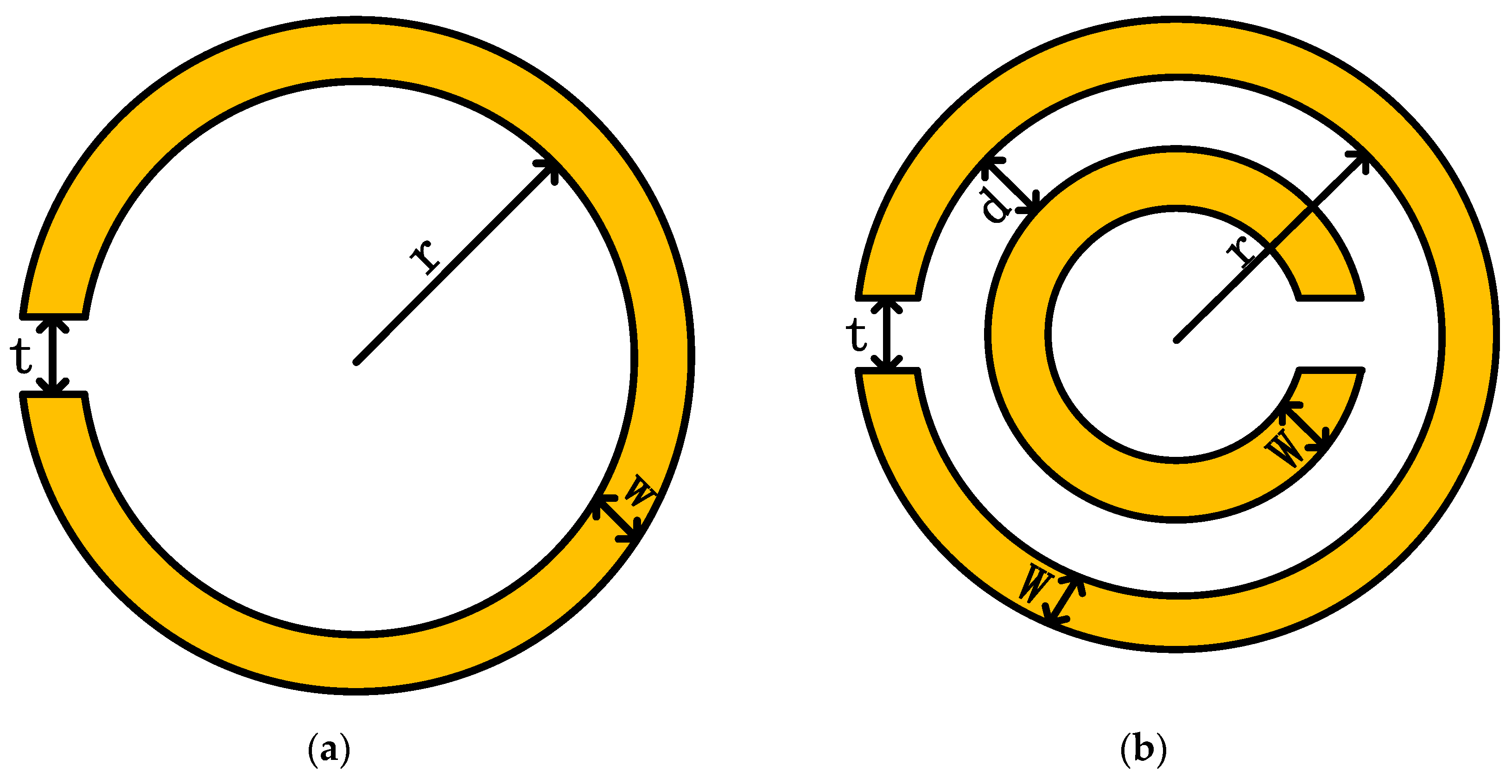
The structures of two types of SRRs are shown in
Figure 1 below.
These two kinds of SRRs have been studied by many researchers [
1,
13], and the same equivalent circuit can be obtained for them, as shown in
Figure 2. A transmission line with a series resistor–inductor–capacitor (R–L–C) circuit was used to analyze them, which was consistent with our simulation and experiment setups. The inductance and capacitance (LC) parameters of SR-SRRs can be obtained [
13,
14] by:
where
is the permeability,
is the permittivity,
r is the inner radius of the split ring, W is the width of the split ring, h is the height of the split-ring resonator, and t is the gap width. The inner radius
r can be obtained using the surface resistance multiplied by the area fraction, as shown below:
where a is the period of the metamaterial, σ is the conductivity of the surface, and
is the surface resistance.
is the area fraction constant, which can be set to 2 for the two surfaces of the metamaterial, and can be optimized if losses from other parts of the SRRs are considered.
The inductor,
L, and resistor,
R, of an EC-SRR are the same as for a SR-SRR, and the capacitor
C can be obtained by:
It should be noted that with a sufficiently large d value, an EC-SRR becomes equivalent to a SR-SRR, and that with a small d value, coupled capacitance is the main factor that influences the resonant frequency.
2.2. Negative Group Delay and Loss
S
11 and S
21 can be obtained from an ABCD matrix of the equivalent circuit as:
where
In this formula,
d is the total length of the transmission line,
β is the propagation constant,
R is the resistance,
L is the inductance,
C is the capacitance, and
w is the angular frequency. The amplitudes of S11 and S21 can be simplified at the resonant frequency as:
The total loss can be obtained by:
The loss increases proportionately with R when R is lower than 2. It should be noted that the loss is included with the return loss, but for transmission metamaterials the transmission power is more important than the absolute loss; therefore, S21 which is the ratio between input power and output power, is the critical parameter to evaluate.
S21 phase and group delays can be simplified at the resonant frequency as:
It can be deduced from Equations (6) and (9) that the amplitude of S21 is determined by R, and the group delay is determined by L and R.
3. Simulation and Measurement Results
3.1. Simulation Results
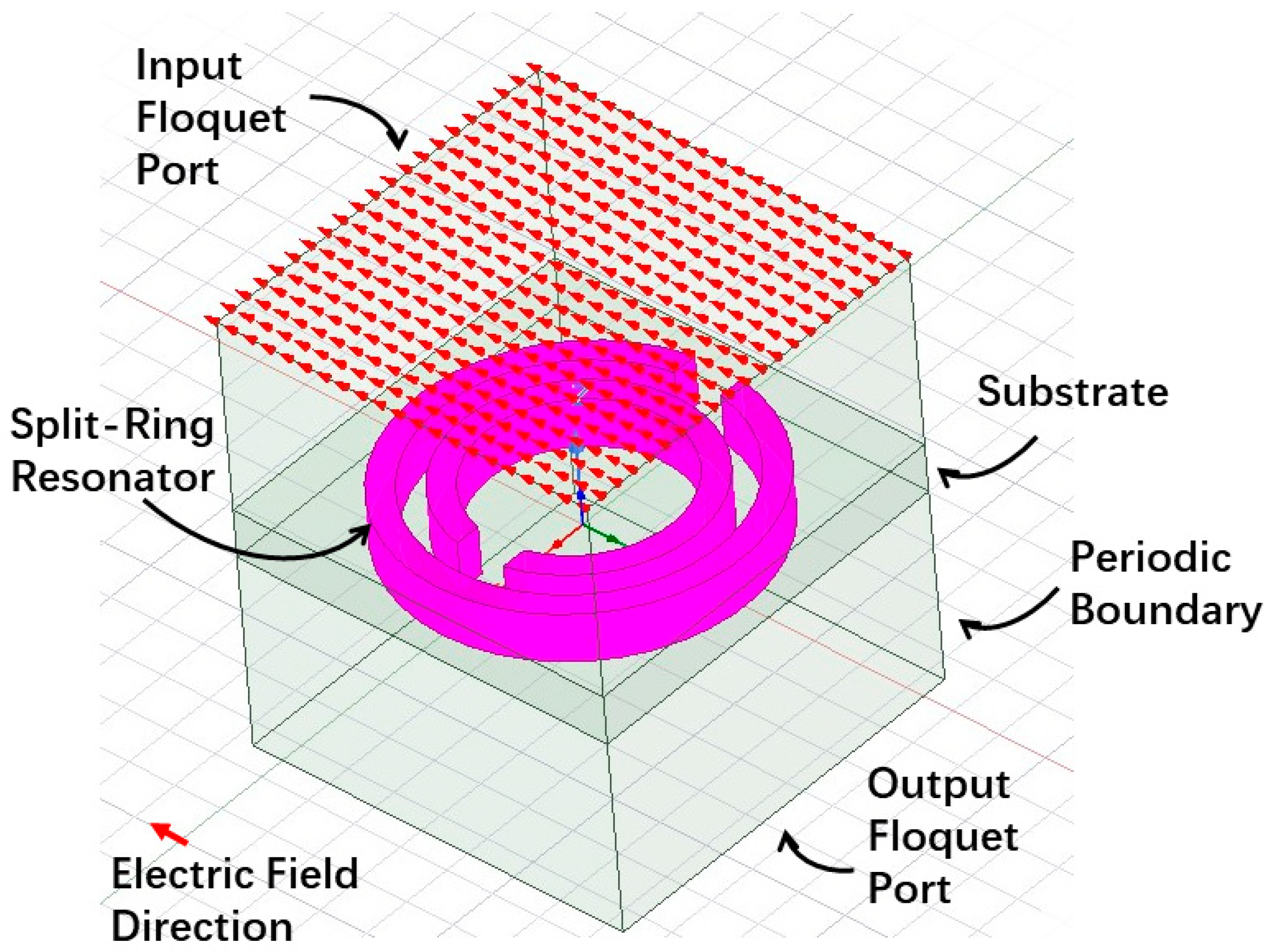
Simulations were conducted using the Ansys HFSS suite (Ansys Inc., Canonsburg, PA, USA). The simulation setup is shown in
Figure 3. The TE
00 mode was used to excite the SRRs; this is same as the transformation metamaterial setup. Teflon substrate was used to as a supporting structure which is widely used and has good electromagnetic properties and the height of which is same as the SRRs. The periodic boundary and the input floquet port are adopted which are used to simulate infinitely large structure and the edge effect can been ignored. The material used for SRRs is tantalum nitride (TaN), and the conductivity is 7400 S/m. The skin depth of the TaN at 15 GHz is 0.04 mm. Therefore, the smallest possible size of the structure should be greater than 0.04 mm and the solving inside threshold of its conductivity was set at 10,000 S/m. It should be noted that the TE
00 mode was used in simulating the metamaterials with periodic boundaries, which is the normal input field mode of metamaterials; however, in measurement setup, the mode of the rectangular waveguide was the TE
10 mode, which may cause a slight difference in resonant frequency compared with TE
00 mode excitation.
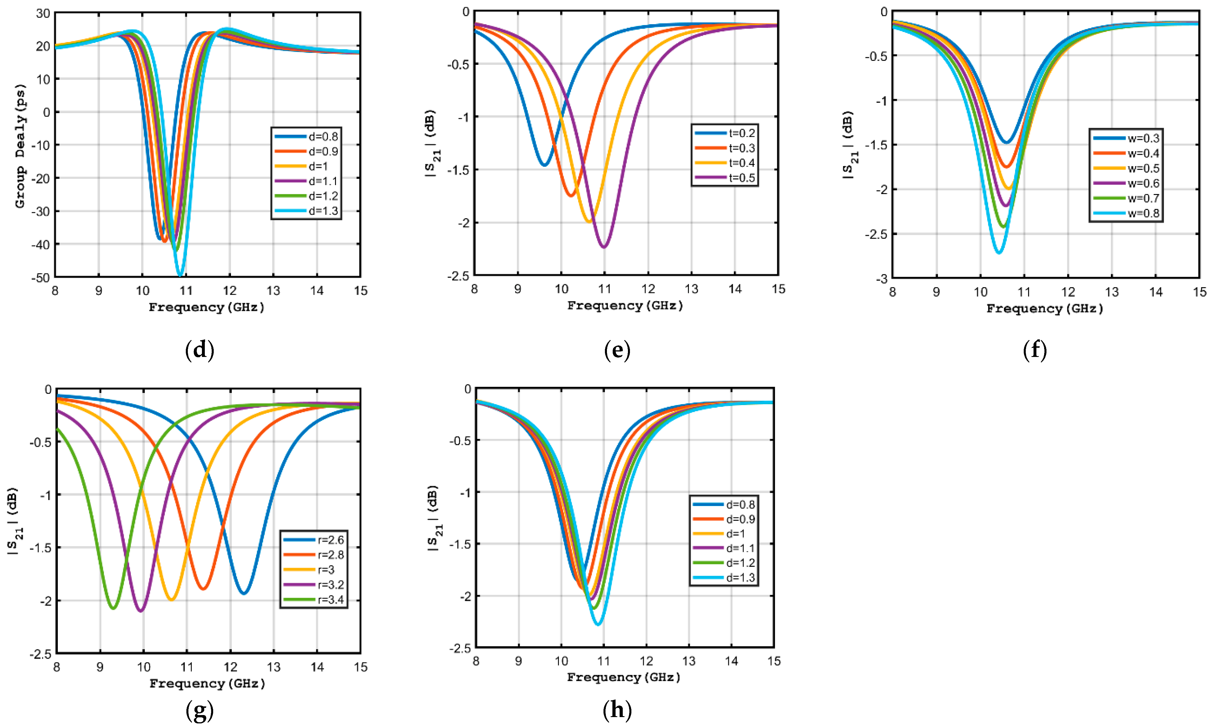
3.1.1. SR-SRR
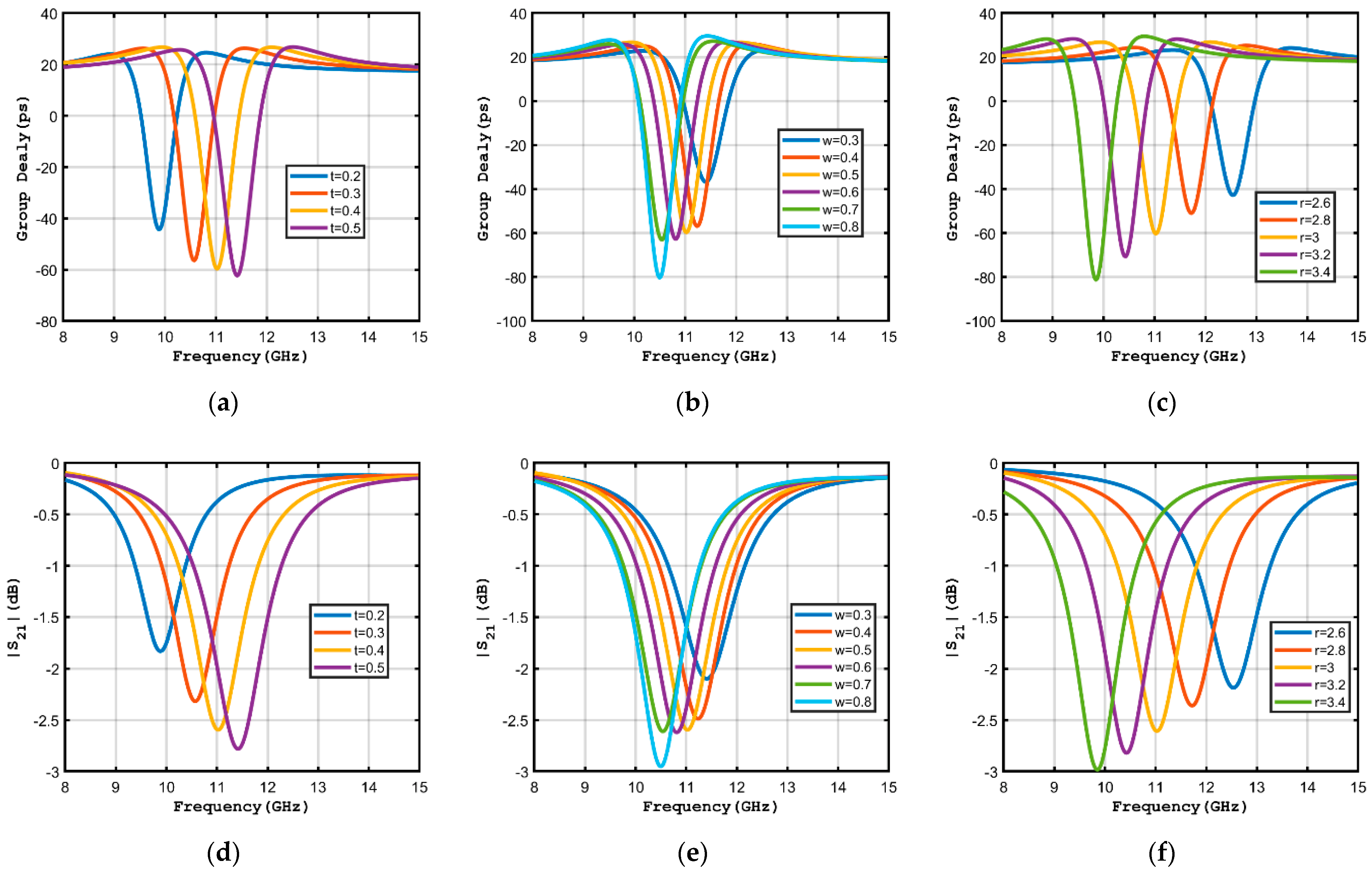
It can be seen from the simulation results (
Figure 4) that as w and r increase, the resonant frequency is reduced, which is due to the increase in
L and
C. The loss increases with the reduction in resonant frequency, which is due to the fact that when r and w increase, the area of the ring increased as well, which in turn increases the loss. When t increases, the
L and
C reduced and then the resonant frequency increases as well. Although the increase in t can reduce the area of the ring to some extent, the increase in the frequency of the surface resistance mainly influences the loss. Additionally, according to Equation (9), the increase in the surface resistance will increase the NGD value.
3.1.2. EC-SRR
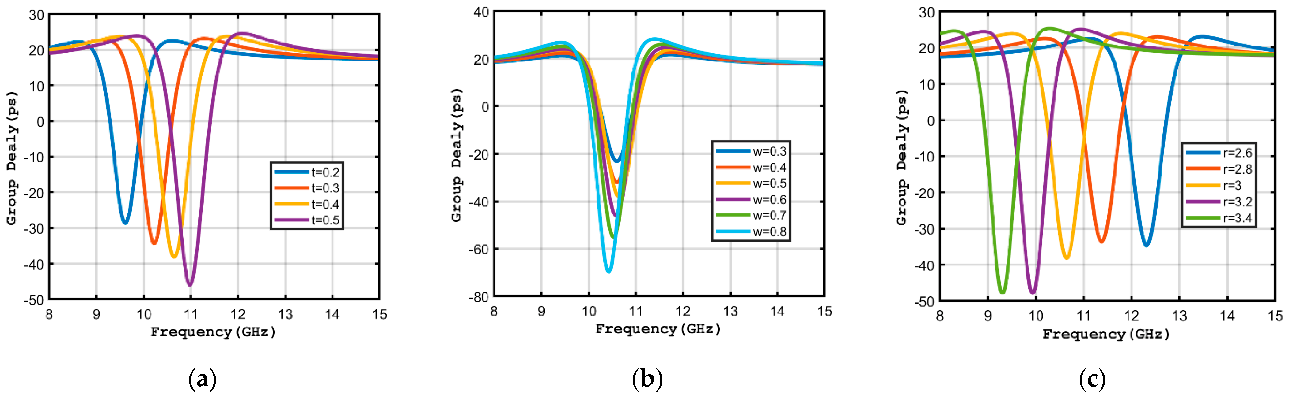
The performances of r, t, and w for EC-SRRs (
Figure 5) are the same as for SR-SRRs, which can be seen from the equivalent circuit of EC-SRRs where the
L term, and part of the
C term, are decided by the outer ring. The only difference between the two is in the d parameter. When d increases, the coupled capacitance between the rings is reduced and the resonant frequency is reduced, which in turn decreases the surface resistance. Additionally, according to Equation (9), the decrease in surface resistance will reduce the NGD value.
3.2. Measured Results
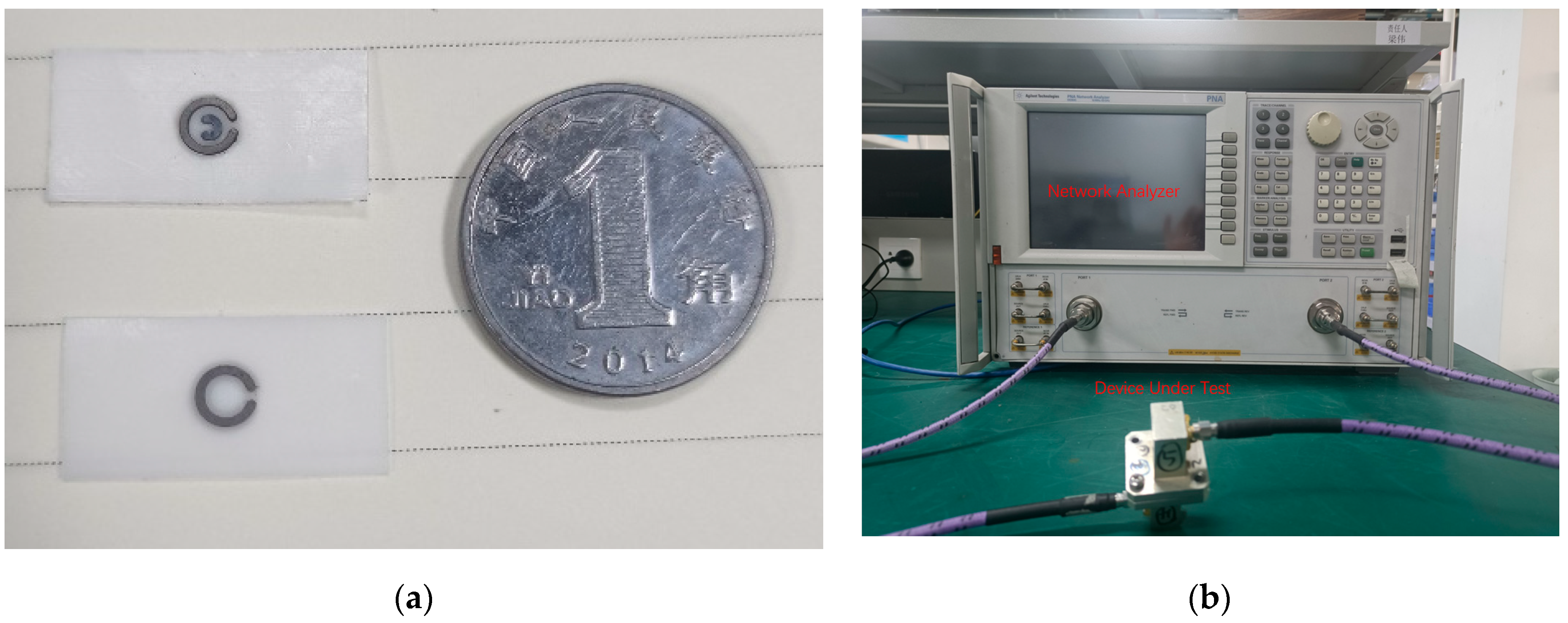
The prototypes of the proposed structures were fabricated (
Figure 6a) and tested using an Agilent E8364C network analyzer (Agilent Technologies Inc., Santa Clara, CA, USA) (
Figure 6b). Due to the high hardness and high machining accuracy requirement of the SRRs, laser cutting was used to process the TaN material, which has a low cost in mass production. Additionally, the Teflon substrate was fabricated using computer numerical control (CNC) machining.
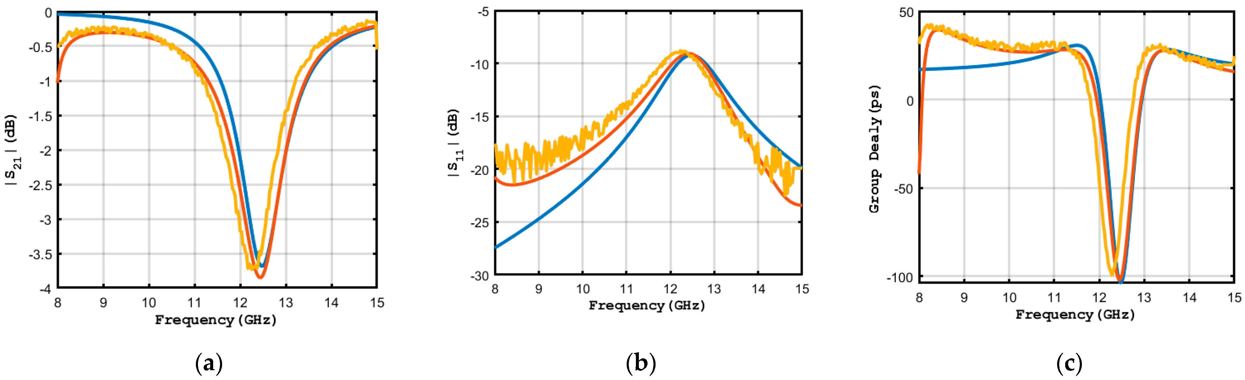
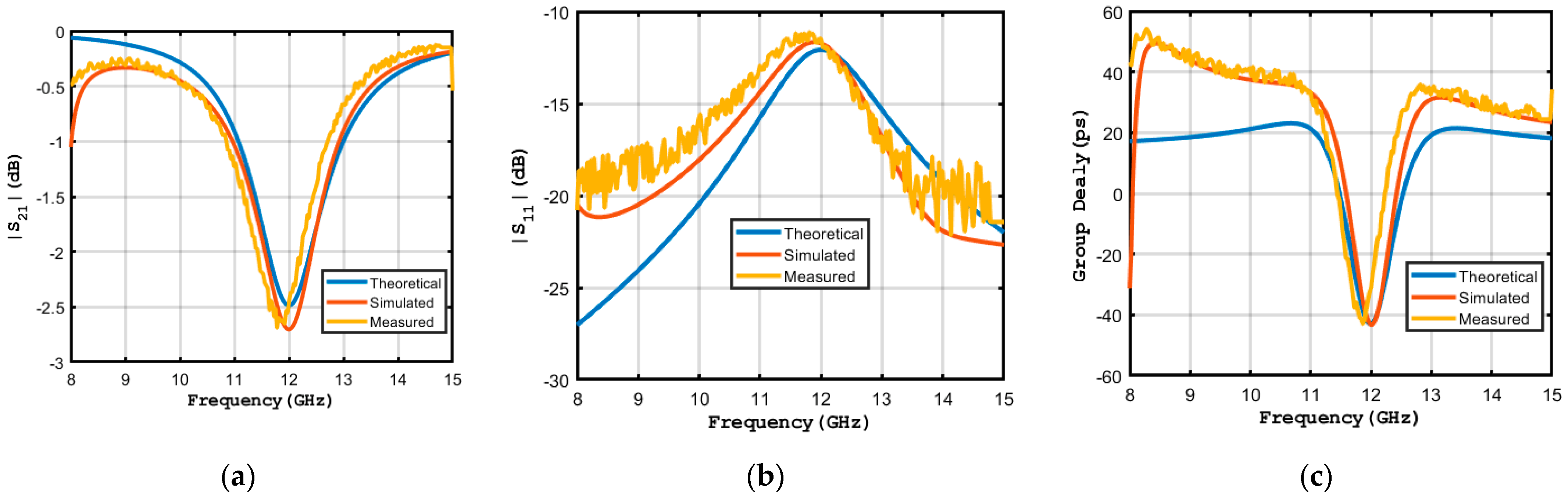
The metamaterials were put into the same type of WR75 rectangular waveguide used [
1]. in their 1999 report which is a widely used measurement setup. The parameters used were: t = 0.5 mm, r = 1.3 mm, w = 0.5 mm, h = 0.3 mm, and d = 0.5 mm. The simulated and measured results are shown in
Figure 7 and
Figure 8, respectively, to illustrate the consistency between them. The simulation was performed in the waveguide condition. The small observed differences may be attributable to the Teflon substrate used in the real-world test, of which the dielectric constant is not stable. The cut-off frequency of WR75 waveguide is 10 GHz, and the S21 and group delay performance below 10 GHz should be ignored. It can be seen from
Figure 7 and
Figure 8 that with the same outer ring dimension, the S21 of the EC-SRR was lower than that of the SR-SRR, due to the reduction in the resonant frequency. The measured S11 was also consistent with the theoretical and simulated predictions.
4. Application
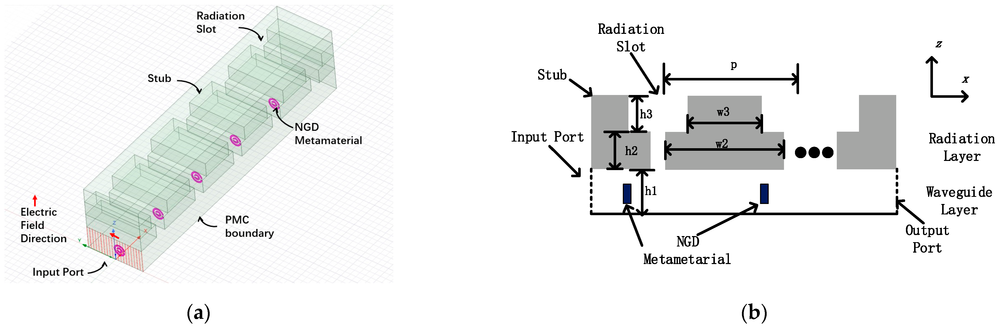
The structure of continuous transverse stub (CTS) antenna is shown in
Figure 9. The antenna comprises two layers: radiation and waveguide layers. The radiation layer is composed of transverse stubs. The electromagnetic power radiates from the slots between the stubs. The waveguide layer and the radiation layer form a parallel plate waveguide structure and antenna aperture.
The beam direction of CTS antenna with
can be detected by
where
is the elevation angle, λ is the wavelength,
is the effective dielectric constant,
is the propagation constant in free space and
is the slot period.
It can be seen from Equation (10) that as the frequency increases the beam direction moves closer to the normal direction. The frequency scanning is caused by the time delay between each slot. Therefore, the NGD can be introduced to reduce the frequency scanning. NGD metamaterial can be placed in the waveguide layer or below the radiation layer, but here only the waveguide situation is discussed and EC-SRR was used. It should be noted that the metamaterial element period should be same as the slot period and the NGD value and frequency should be adjusted using the metamaterial parameters.
Simulations of the proposed CTS antenna were conducted using the Ansys HFSS suite (Ansys Inc., Canonsburg, PA, USA). The boundaries of the two sides are set using the perfect magnetic conductor (PMC), which are the same as for the CTS antenna, and the TEM mode is generated in the waveguide. For the CTS antenna, the TEM mode feed can be achieved by linear source generator. CTS antenna with five slots was simulated. The parameters were h1 = 8 mm, h2 = 5 mm, h3 = 5 mm, p = 19 mm, h2 = 5 mm, w2 = 15 mm, w3 = 11 mm, r = 1.5 mm, t = 0.5 mm, w = 0.5 mm, h = 0.1 mm, and d = 0.5 mm.
The simulated E-plane patterns of the CTS antenna are shown in
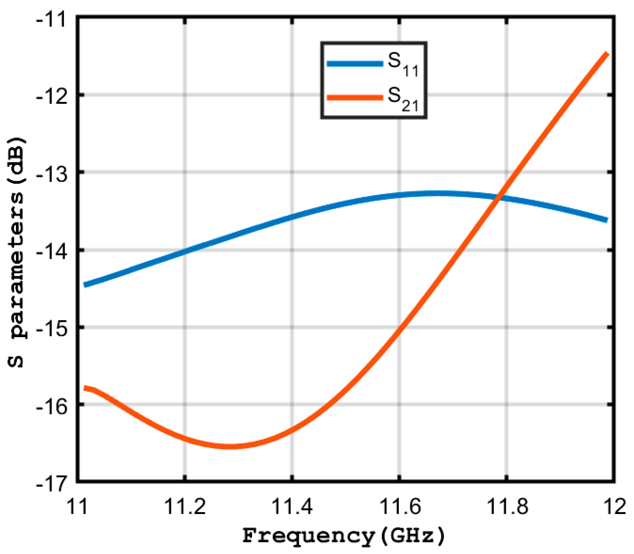
Figure 10. The beam walk reduction can be observed. The simulated S parameters are shown in
Figure 11. S
11 and S
21 are both below −12 dB.
It should be noted that although the frequency scanning can be reduced with the introduction of the NGD metamaterial, the gain of the antenna also reduced. Additionally, because the gain varies with frequency, the instantaneous bandwidth may also be reduced. However, this issue can be resolved using the wideband flat NGD device.
5. Conclusions
In this report, negative group delay (NGD) metamaterials based on split-ring resonators (SRRs) were evaluated. A theoretical analysis was first performed to obtain the equivalent circuit parameters, NGD values, and S21 amplitudes. The parameters were then simulated and discussed, and the metamaterials were fabricated from tantalum nitride before being tested in a laboratory setting. The measured results were found to be consistent with the theoretical and simulated predictions. For EC-SRR, a negative group delay of up to −0.1 ns was achieved at 12–13 GHz. For SR-SRR of the same size as the out ring of EC-SRR, a negative group delay of up to −0.04 ns was achieved with a loss lower than 2.7 dB. The application of the metamaterial was discussed, and the frequency scanning reduction in CTS antenna was achieved using NGD metamaterials.
Author Contributions
Conceptualization, Z.L. and J.Z.; methodology, X.L.; software, J.G.; validation, T.L.; formal analysis, Z.X.; investigation, Z.L.; resources, Z.L.; data curation, Z.L.; writing—original draft preparation, Z.L.; writing—review and editing, Z.L.; visualization, Z.L.; supervision, Z.L.; project administration, Z.L. All authors have read and agreed to the published version of the manuscript.
Funding
The authors have no funding sources to declare.
Data Availability Statement
The data presented in this study are available on request from the corresponding author.
Conflicts of Interest
The authors declare no conflict of interest.
References
- Pendry, J.B.; Holden, A.J.; Robbins, D.J.; Stewart, W.J. Magnetism from conductors and enhanced nonlinear phenomena. IEEE Trans. Microw. Theory Tech. 1999, 47, 2075–2084. [Google Scholar] [CrossRef]
- Chen, Z.; Tang, M.-C.; Li, M.; Su, M. Far-Field Decoupling of Two-Element Antenna Transceiving System by the Periodic Near-Field Resonators. IEEE Antennas Wirel. Propag. Lett. 2022, 21, 2065–2069. [Google Scholar] [CrossRef]
- Huang, D.; Xu, G.; Wu, J.; Wang, W.; Yang, L.; Huang, Z.-X.; Wu, X.-L.; Yin, W.-Y. A Microstrip Dual-Split-Ring Antenna Array for 5G Millimeter-Wave Dual-Band Applications. IEEE Antennas Wirel. Propag. Lett. 2022, 21, 2025–2029. [Google Scholar] [CrossRef]
- Monti, G.; Tarricone, L. Negative Group Velocity In A Split Ring Resonator-Coupled Microstrip Line. Prog. Electromagn. Res. 2009, 94, 33–47. [Google Scholar] [CrossRef]
- Woodley, J.F.; Mojahedi, M. Negative group velocity and group delay in left-handed media. Phys. Rev. E 2004, 70, 046603. [Google Scholar] [CrossRef] [PubMed]
- Das, P.; Mandal, K.; Lalbakhsh, A. Beamsteering of microstrip antenna using single-layer FSS based phase-shifting surface. Int. J. RF Microw. Comput.-Aided Eng. 2022, 32, e23033. [Google Scholar] [CrossRef]
- Liang, Y.; Koshelev, K.; Zhang, F.; Lin, H.; Lin, S.; Wu, J.; Jia, B.; Kivshar, Y. Bound States in the Continuum in Anisotropic Plasmonic Metasurfaces. Nano Lett. 2020, 20, 6351–6356. [Google Scholar] [CrossRef] [PubMed]
- Lalbakhsh, A.; Afzal, M.U.; Esselle, K.P.; Smith, S.L. All-Metal Wideband Frequency-Selective Surface Bandpass Filter for TE and TM Polarizations. IEEE Trans. Antennas Propag. 2022, 70, 2790–2800. [Google Scholar] [CrossRef]
- Brillouin, L.; Chako, N. Wave Propagation and Group Velocity; Academic press: New York, NY, USA, 1960. [Google Scholar] [CrossRef]
- Takeda, S.; Anada, T. Phase equalizer making use of negative group delay times by reflection coefficients. In Proceedings of the 41st European Mi-crowave Conference 2011, Manchester, UK, 10–13 October 2011; pp. 627–630. [Google Scholar]
- Chaudhary, G.; Park, J.; Wang, Q.; Jeong, Y. A design of unequal power divider with positive and negative group delays. In Proceedings of the 2015 European Microwave Conference (EuMC), Paris, France, 7–10 September 2015; pp. 127–130. [Google Scholar] [CrossRef]
- Ahn, K.-P.; Ishikawa, R.; Honjo, K. Group Delay Equalized UWB InGaP/GaAs HBT MMIC Amplifier Using Negative Group Delay Circuits. IEEE Trans. Microw. Theory Tech. 2009, 57, 2139–2147. [Google Scholar] [CrossRef]
- Froncisz, W.; Hyde, J.S. The loop-gap resonator: A new microwave lumped circuit ESR sample structure. J. Magn. Reson. 1982, 47, 515–521. [Google Scholar] [CrossRef]
- Roshani, S.; Azizian, J.; Roshani, S.; Jamshidi, M.; Parandin, F. Design of a miniaturized branch line microstrip coupler with a simple structure using artificial neural network. Frequenz 2022, 76, 255–263. [Google Scholar] [CrossRef]
| Disclaimer/Publisher’s Note: The statements, opinions and data contained in all publications are solely those of the individual author(s) and contributor(s) and not of MDPI and/or the editor(s). MDPI and/or the editor(s) disclaim responsibility for any injury to people or property resulting from any ideas, methods, instructions or products referred to in the content. |
© 2023 by the authors. Licensee MDPI, Basel, Switzerland. This article is an open access article distributed under the terms and conditions of the Creative Commons Attribution (CC BY) license (https://creativecommons.org/licenses/by/4.0/).


