
A 3.4–3.6 GHz High-Selectivity Filter Chip Based on Film Bulk Acoustic Resonator Technology


Abstract
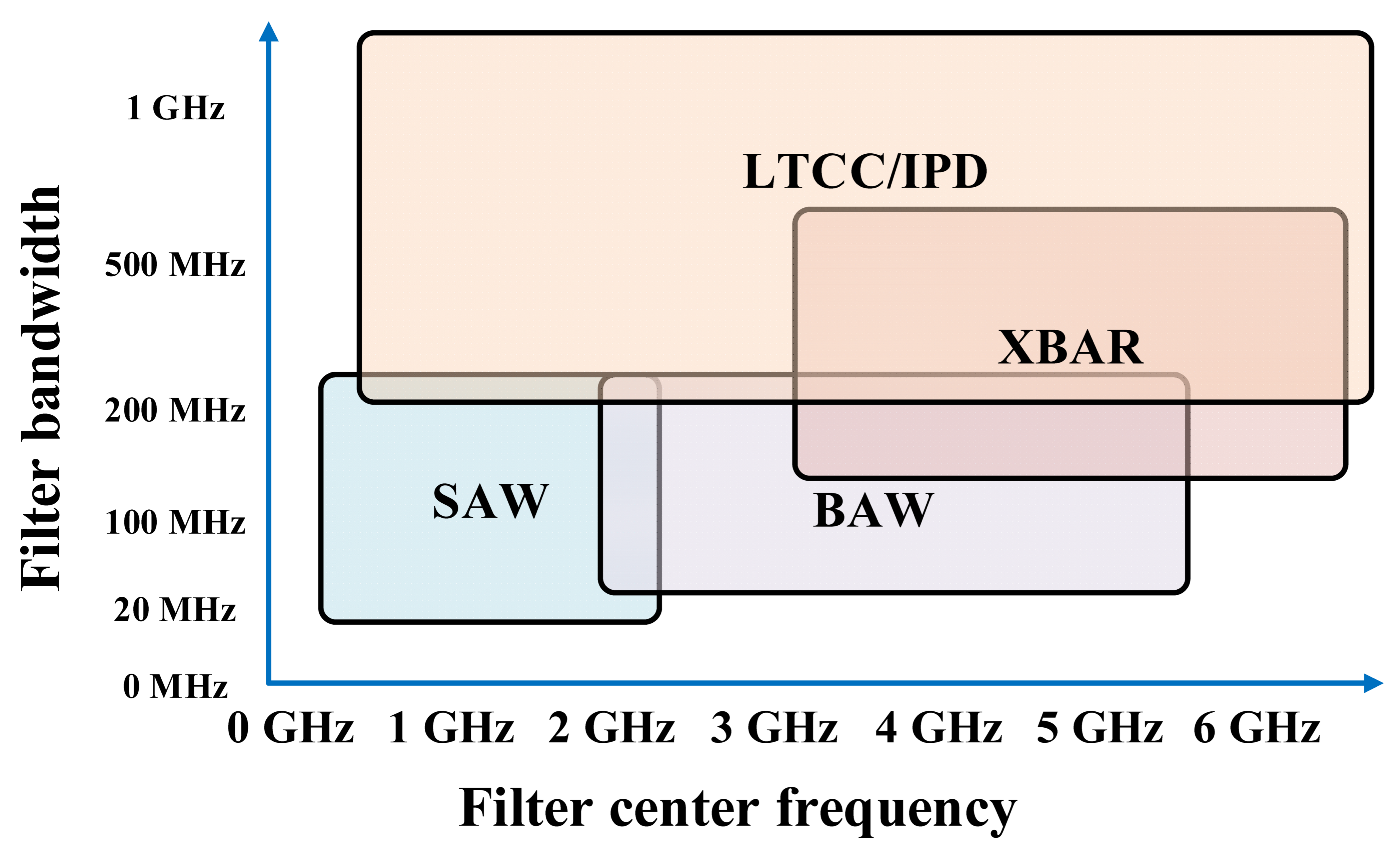
:1. Introduction
2. Model Fitting of FBAR
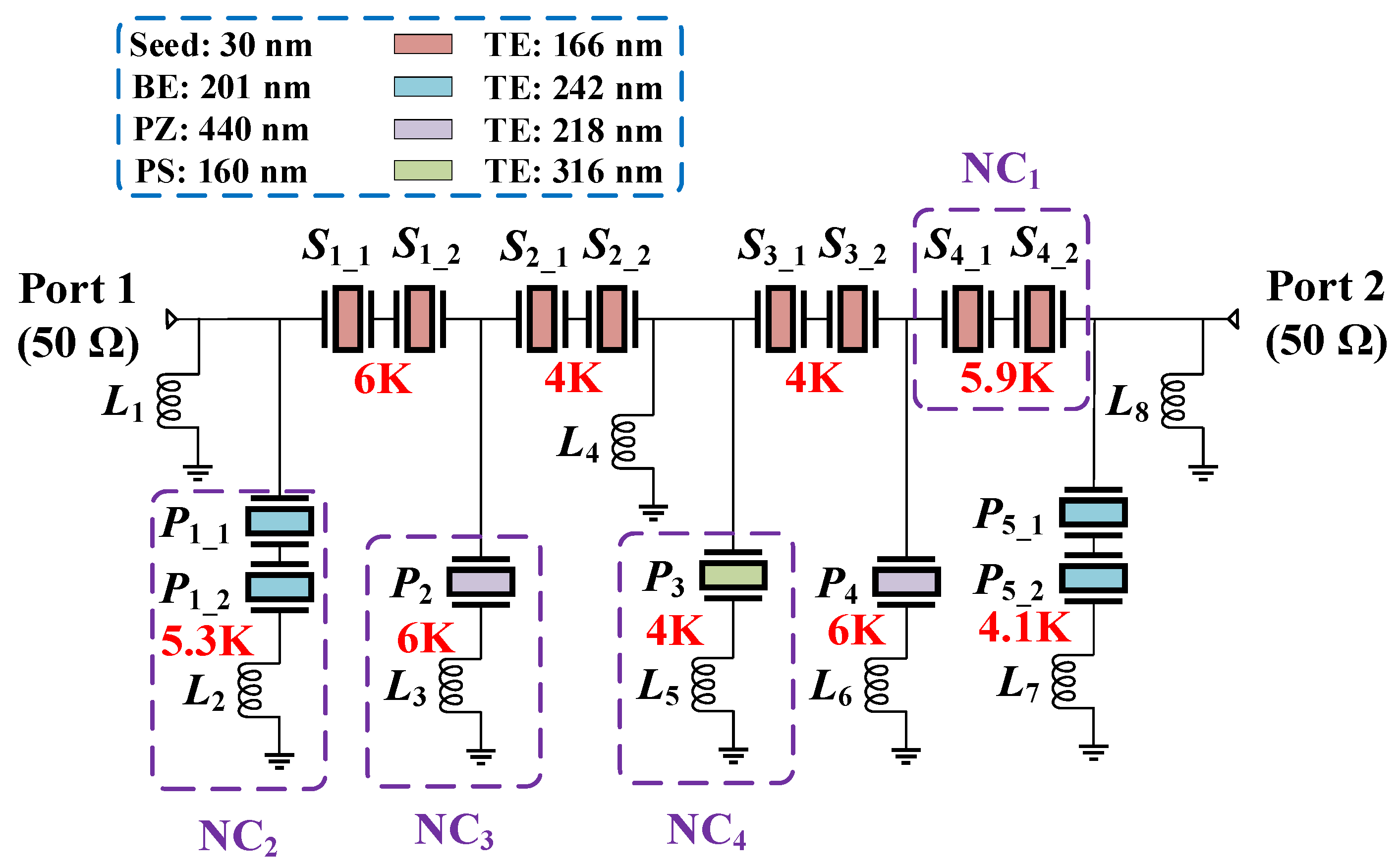
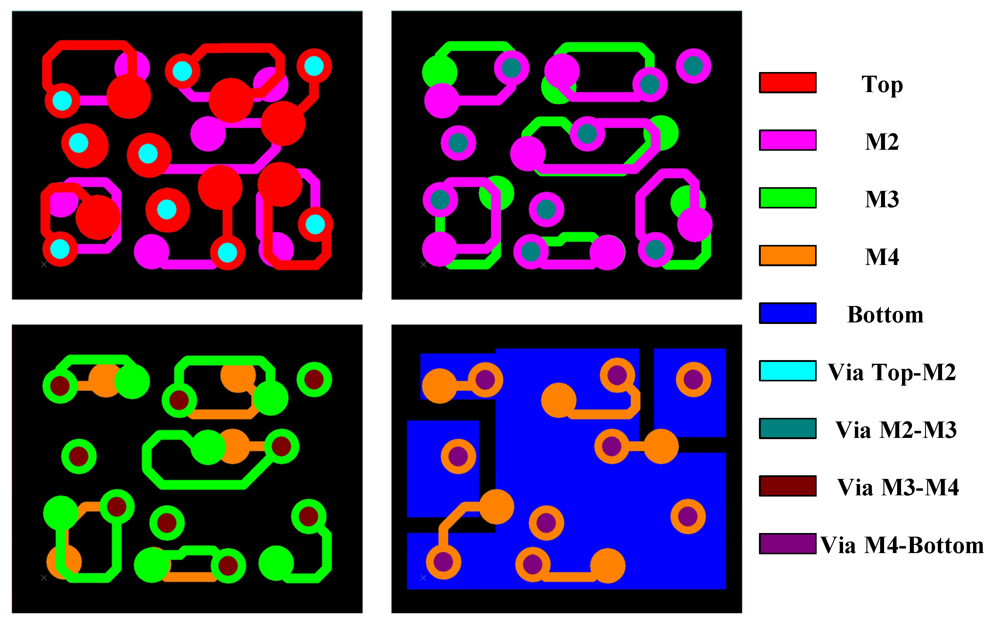
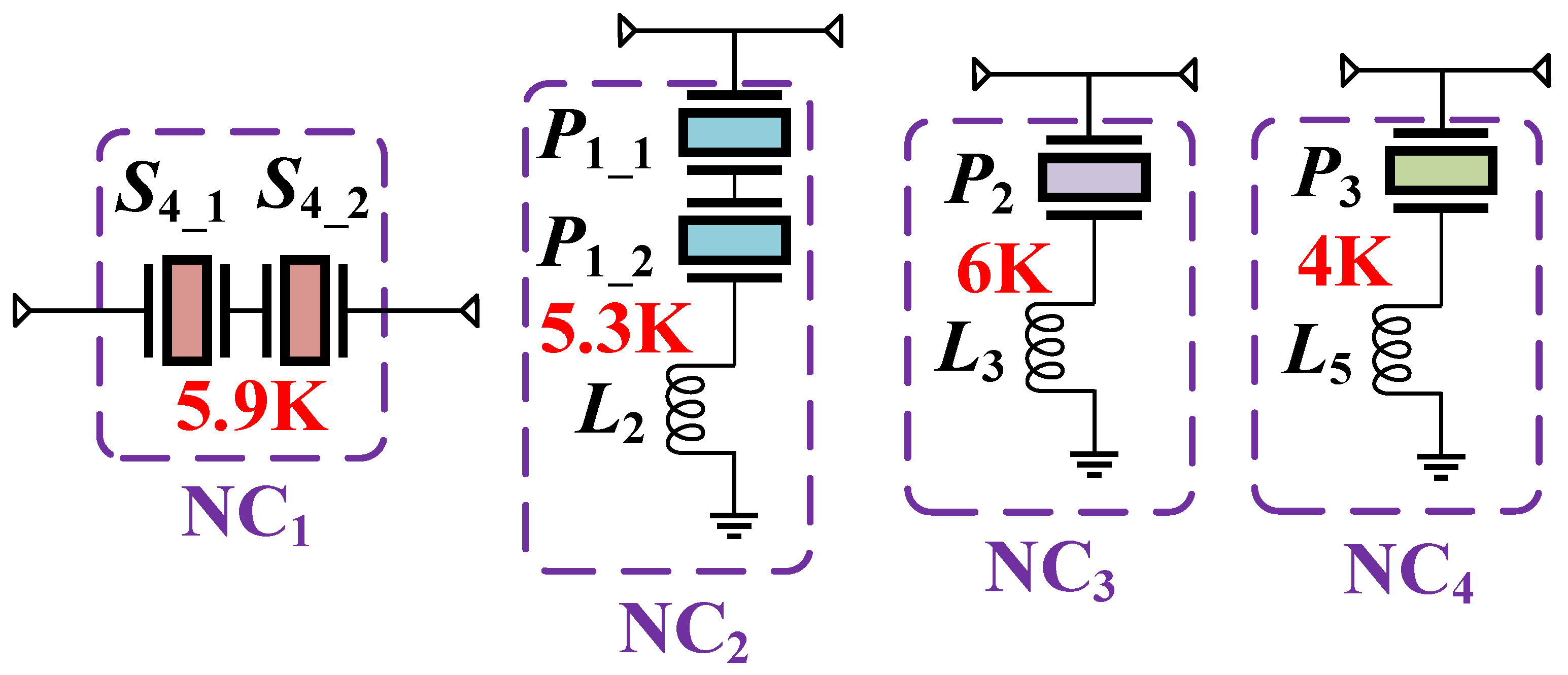
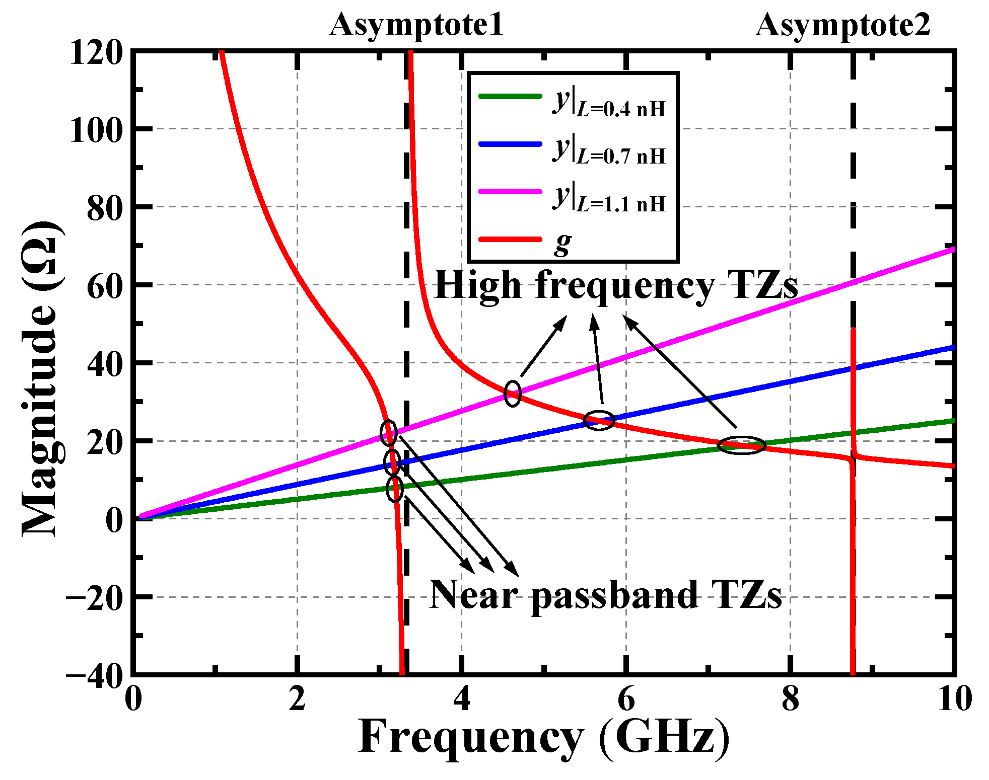
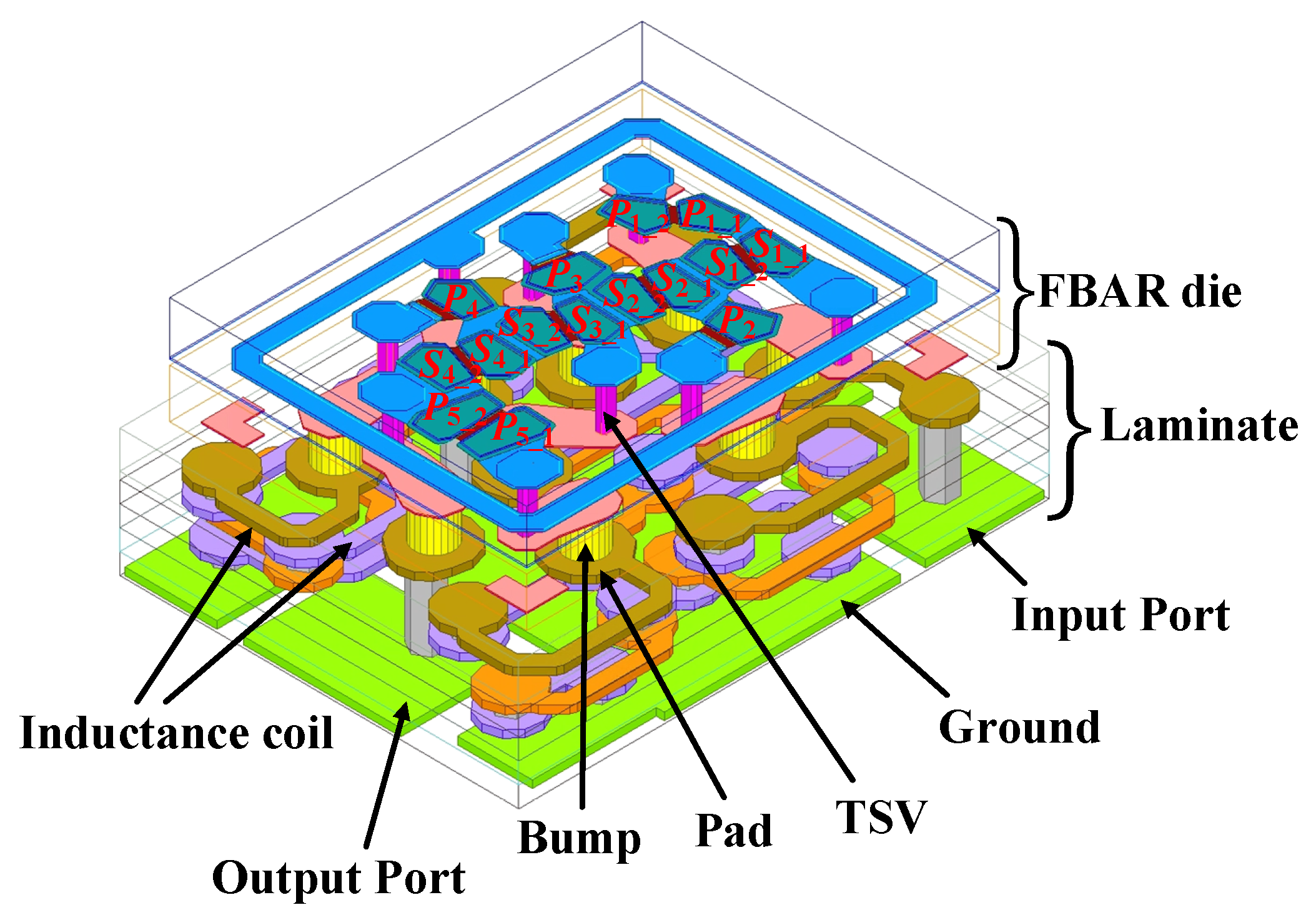
3. Design and Analysis of the FBAR Filter
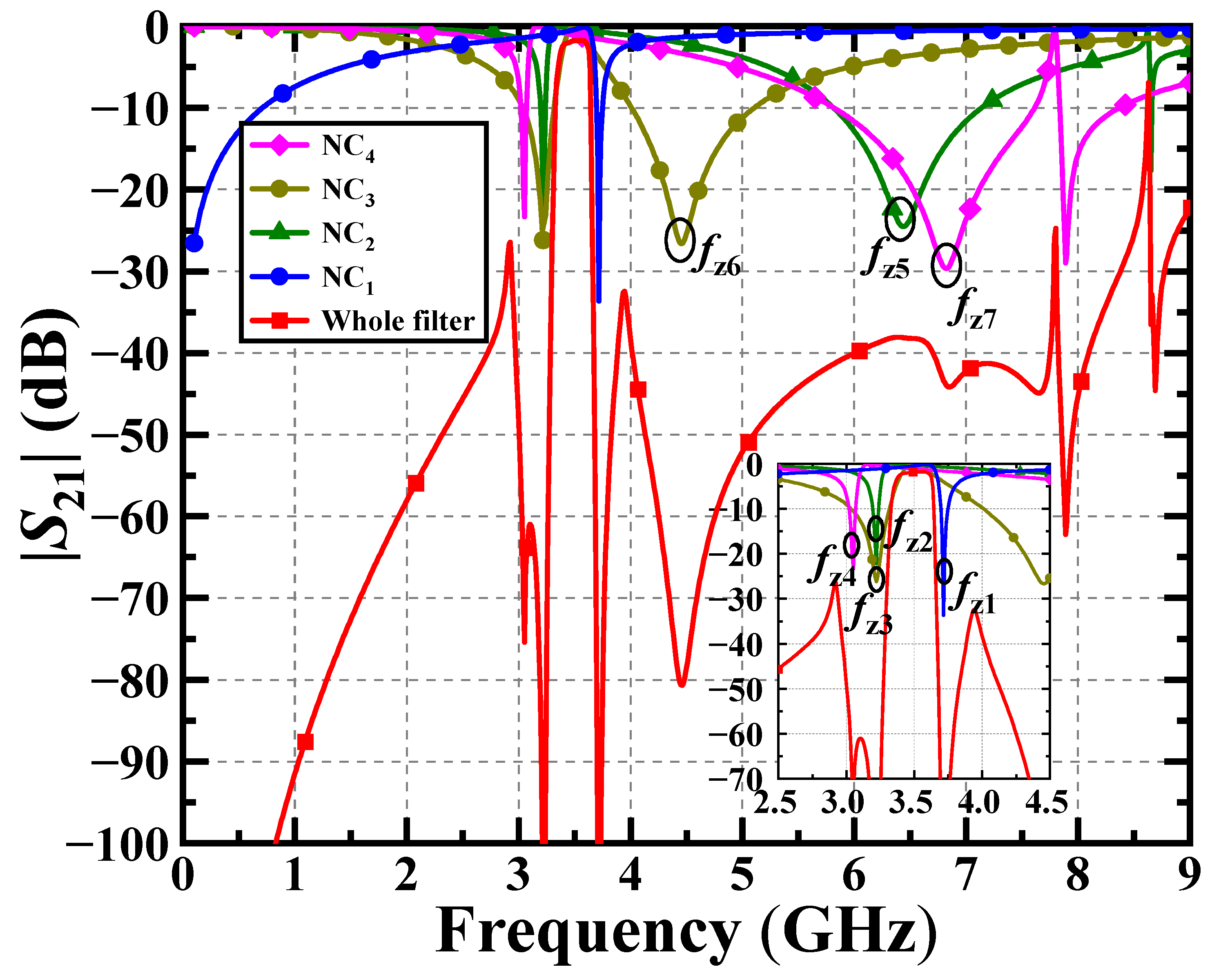
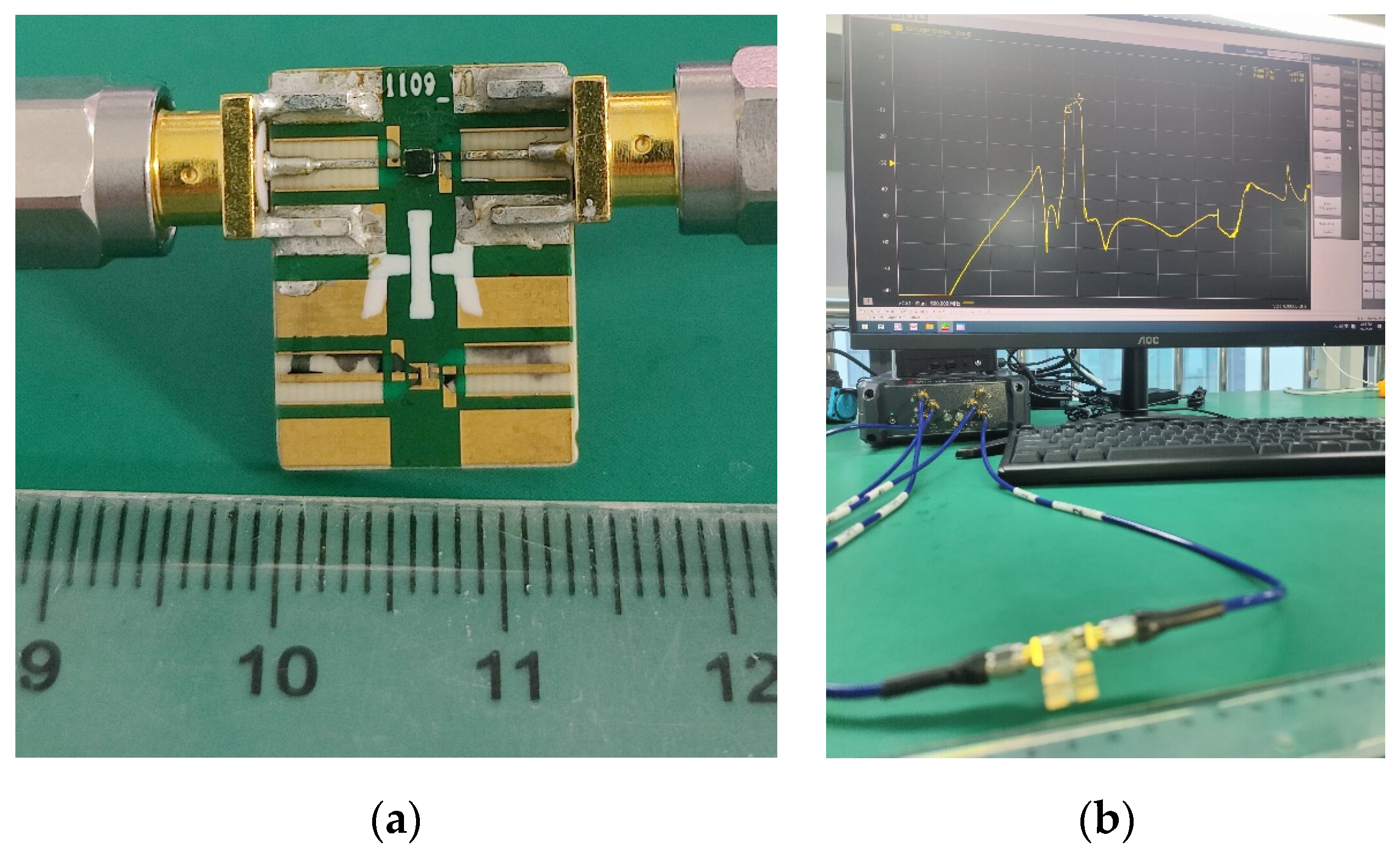
4. EM Simulation and Measured Results
5. Conclusions
Author Contributions
Funding
Data Availability Statement
Acknowledgments
Conflicts of Interest
References
- Li, Z.; Cheng, G.; Wang, Z. A 0.1–1 GHz low power RF receiver front-end with noise cancellation technique for WSN applications. AEU—Int. J. Electron. Commun. 2018, 83, 288–294. [Google Scholar] [CrossRef]
- Roshani, S.; Dehghani, K.; Roshani, S. A Lowpass Filter Design Using Curved and Fountain Shaped Resonators. Frequenz 2019, 73, 267–272. [Google Scholar] [CrossRef]
- Hookari, M.; Roshani, S.; Roshani, S. Design of a low pass filter using rhombus-shaped resonators with an analytical LC equivalent circuit. Turk. J. Electr. Eng. Comput. Sci. 2020, 28, 865–874. [Google Scholar] [CrossRef]
- Psychogiou, D.; Gómez-García, R.; Peroulis, D. Single and Multiband Acoustic-Wave-Lumped-Element-Resonator (AWLR) Bandpass Filters with Reconfigurable Transfer Function. IEEE Trans. Microw. Theory Tech. 2016, 64, 4394–4404. [Google Scholar] [CrossRef]
- Hao, L.; Wu, Y.; Wang, W.; Yang, Y. Design of On-Chip Dual-Band Bandpass Filter Using Lumped Elements in LTCC Technology. IEEE Trans. Circuits Syst. II Express Briefs 2022, 69, 959–963. [Google Scholar] [CrossRef]
- Xu, Y.; Wu, Y.; Wu, H.; Yang, Y.; Wang, W. Wideband High Selectivity Filter Chips with Adjustable Bandwidth Based on IPD Technology. IEEE Trans. Circuits Syst. II Express Briefs 2022, 69, 4273–4277. [Google Scholar] [CrossRef]
- Yandrapalli, S.; Plessky, V.; Koskela, J.; Yantchev, V.; Turner, P.; Villanueva, L.G. Analysis of XBAR resonance and higher order spurious modes. In Proceedings of the IEEE International Ultrasonics Symposium, Glasgow, UK, 6–9 October 2019. [Google Scholar]
- Plessky, V.; Yandrapalli, S.; Turner, P.J.; Villanueva, L.G.; Koskela, J.; Faizan, M.; De Pastina, A.; Garcia, B.; Costa, J.; Hammond, R.B. Laterally excited bulk wave resonators (XBARs) based on thin Lithium Niobate platelet for 5GHz and 13 GHz filters. In Proceedings of the IEEE MTT-S International Microwave Symposium, Boston, MA, USA, 2–7 June 2019. [Google Scholar]
- Lee, S.; Lee, V.; Sis, A.; Mortazawi, A. A simple nonlinear mBVD model parameter extraction method for intrinsically switchable ferroelectric FBARs. In Proceedings of the European Microwave Integrated Circuit Conference, Nuremberg, Germany, 6–8 October 2013. [Google Scholar]
- Yokoyama, T.; Iwazaki, Y.; Onda, Y.; Nishihara, T.; Ueda, M. Highly piezoelectric co-doped AlN thin films for wideband FBAR applications. IEEE Trans. Ultrason. Ferroelectr. Freq. Control 2015, 62, 1007–1015. [Google Scholar] [CrossRef] [PubMed]
- Wu, H.; Cai, X.; Wu, Y.; Lai, Z.; Yang, Q.; Wang, W. An investigation on extraction of material parameters in longitudinal mode of FBAR. IEEE Trans. Circuits Syst. II Express Briefs 2020, 67, 1024–1028. [Google Scholar] [CrossRef]
- Ruby, R.; Gilbert, S.; Lee, S.K.; Nilchi, J.; Kim, S.W. Novel Temperature-Compensated, Silicon SAW Design for Filter Integration. IEEE Microw. Wirel. Compon. Lett. 2021, 31, 674–677. [Google Scholar] [CrossRef]
- Wu, Y.; Wu, H.; Wang, W.; Yang, Y.; Lai, Z.; Yang, Q. A Compact Low-Loss High-Selectivity Excellent-Isolation FBAR Duplexer Integrated Chip for LTE Band-3 Industrial Applications. IEEE Trans. Circuits Syst. II Express Briefs 2022, 69, 4563–4567. [Google Scholar] [CrossRef]
- Wu, H.; Wu, Y.; Lai, Z.; Wang, W.; Yang, Q. A Hybrid Film-Bulk-Acoustic-Resonator/Coupled-Line/Transmission-Line High Selectivity Wideband Bandpass FBAR Filter. IEEE Trans. Microw. Theory Tech. 2020, 68, 3389–3396. [Google Scholar] [CrossRef]
- Jamneala, T.; Bradley, P.; Koelle, U.B.; Chien, A. Modified Mason model for bulk acoustic wave resonators. IEEE Trans. Ultrason. Ferroelectr. Freq. Control 2008, 55, 2025–2029. [Google Scholar] [CrossRef] [PubMed]
- Pozar, D.M. Microwave Engineering, 2nd ed.; Wiley: New York, NY, USA, 1997. [Google Scholar]
- Shealy, J.B.; Vetury, R.; Gibb, S.R.; Hodge, M.D.; Patel, P.; McLain, M.A.; Feldman, A.Y.; Boomgarden, M.D.; Lewis, M.P.; Hosse, B.; et al. Low loss, 3.7 GHz wideband BAW filters, using high power single crystal AlN-on-SiC resonators. In Proceedings of the IEEE MTT-S International Microwave Symposium, Honololu, HI, USA, 4–9 June 2017. [Google Scholar]
- Gu, J.; Wu, Y.; Lai, Z.; Wu, H.; Wang, W.; Yang, Y. An N41-Band Bandpass BAW Filter Chip for Mobile Communications Based on FBARs. In Proceedings of the 2020 IEEE Asia-Pacific Microwave Conference, Hong Kong, China, 8–11 December 2020. [Google Scholar]
- Bogner, A.; Bauder, R.; Timme, H.J.; Forster, T.; Reccius, C.; Weigel, R.; Hagelauer, A. Enhanced Piezoelectric AL1−XSCXN RF-MEMS Resonators for Sub-6 GHz RF-Filter Applications: Design, Fabrication and Characterization. In Proceedings of the 2020 IEEE 33rd International Conference on Micro Electro Mechanical Systems, Vancouver, BC, Canada, 18–22 January 2020. [Google Scholar]
- Shen, Y.; Zhang, R.; Vetury, R.; Shealy, J. 40.6 Watt, High Power 3.55 GHz Single Crystal XBAW RF Filters for 5G Infrastructure Applications. In Proceedings of the IEEE International Ultrasonics Symposium, Las Vegas, NV, USA, 7–11 September 2020. [Google Scholar]
- Kimura, T.; Omura, M.; Kishimoto, Y.; Hashimoto, K. Comparative Study of Acoustic Wave Devices Using Thin Piezoelectric Plates in the 3–5-GHz Range. IEEE Trans. Microw. Theory Tech. 2019, 67, 915–921. [Google Scholar] [CrossRef]
- Su, R.; Fu, S.; Shen, J.; Lu, Z.; Xu, H.; Wang, R.; Song, C.; Zeng, F.; Wang, W.; Pan, F. Wideband Surface Acoustic Wave Filter at 3.7 GHz with Spurious Mode Mitigation. IEEE Trans. Microw. Theory Tech. 2022, 71, 480–487. [Google Scholar] [CrossRef]


| Seed (nm) | BE (nm) | PZ (nm) | TE (nm) | PS (nm) | fp 1 (MHz) | |
|---|---|---|---|---|---|---|
| Resonator 1 | 30.8 | 234.0 | 447.0 | 218.5 | 141.5 | 3217.2 |
| Resonator 2 | 27.8 | 233.7 | 449.0 | 217.0 | 148.0 | 3231.6 |
| Resonator 3 | 32.1 | 233.7 | 446.3 | 217.7 | 148.0 | 3220.0 |
| Resonator 4 | 29.5 | 230.3 | 448.0 | 217.0 | 140.3 | 3223.8 |
| Longitudinal Acoustic Velocity (m/s) | Density (kg/m3) | |||
|---|---|---|---|---|
| AlN | Mo | AlN | Mo | |
| Original | 10,886 | 5954 | 3270 | 9803 |
| Modified | 10,690.3 | 6240.7 | 3422.8 | 11,131.0 |
| kteff 1 | fs 2 (GHz) | fp 3 (GHz) | Qs 4 | Qp 5 | |
|---|---|---|---|---|---|
| Measured S1_1 | 0.0845 | 3.547 | 3.672 | 278 | 960 |
| Simulated S1_1 | 0.0765 | 3.598 | 3.717 | 784 | 1385 |
| Measured S2_1 | 0.0794 | 3.578 | 3.701 | 425 | 733 |
| Simulated S2_1 | 0.0765 | 3.598 | 3.717 | 665 | 1407 |
| Ref. | Type | fc 1 (GHz) | IL 2 (dB) | BW 3 (MHz) | FOM 4 | Stopband Suppression 5 (dB) | Size |
|---|---|---|---|---|---|---|---|
| [17] | FBAR | 3.71 | 3.04 | 120 | 30.92 | 37 | 1.25 × 0.9 mm2/0.015 × 0.011 λ02 |
| [18] | FBAR | 2.6 | 1.7 | 120 | 21.67 | 35 | 1.1 × 0.9 mm2/0.0095 × 0.0078 λ02 |
| [19] | FBAR | 2.45 | 2.5 | 150 | 16.33 | 25 | 1.1 × 0.9 mm2/0.0089 × 0.0074 λ02 |
| [20] | XBAR | 3.55 | 1.4 | 120 | 29.58 | 30 | 1 × 1 mm2/0.012 × 0.012 λ02 |
| [21] | SAW | 3.44 | 1.3 | 200 | 17.2 | 30 | |
| [22] | SAW | 3.74 | 3.03 | 500 | 7.48 | 20 | |
| This work | FBAR | 3.52 | 3.1 | 200 | 17.6 | 35 | 1.1 × 0.9 mm2/0.013 × 0.011 λ02 |
Disclaimer/Publisher’s Note: The statements, opinions and data contained in all publications are solely those of the individual author(s) and contributor(s) and not of MDPI and/or the editor(s). MDPI and/or the editor(s) disclaim responsibility for any injury to people or property resulting from any ideas, methods, instructions or products referred to in the content. |
© 2023 by the authors. Licensee MDPI, Basel, Switzerland. This article is an open access article distributed under the terms and conditions of the Creative Commons Attribution (CC BY) license (https://creativecommons.org/licenses/by/4.0/).
Share and Cite
Yang, Q.; Xu, Y.; Wu, Y.; Wang, W.; Lai, Z. A 3.4–3.6 GHz High-Selectivity Filter Chip Based on Film Bulk Acoustic Resonator Technology. Electronics 2023, 12, 1056. https://doi.org/10.3390/electronics12041056
Yang Q, Xu Y, Wu Y, Wang W, Lai Z. A 3.4–3.6 GHz High-Selectivity Filter Chip Based on Film Bulk Acoustic Resonator Technology. Electronics. 2023; 12(4):1056. https://doi.org/10.3390/electronics12041056
Chicago/Turabian StyleYang, Qinghua, Yao Xu, Yongle Wu, Weimin Wang, and Zhiguo Lai. 2023. "A 3.4–3.6 GHz High-Selectivity Filter Chip Based on Film Bulk Acoustic Resonator Technology" Electronics 12, no. 4: 1056. https://doi.org/10.3390/electronics12041056
APA StyleYang, Q., Xu, Y., Wu, Y., Wang, W., & Lai, Z. (2023). A 3.4–3.6 GHz High-Selectivity Filter Chip Based on Film Bulk Acoustic Resonator Technology. Electronics, 12(4), 1056. https://doi.org/10.3390/electronics12041056