Communication

Correlation of Crystal Defects with Device Performance of AlGaN/GaN High-Electron-Mobility Transistors Fabricated on Silicon and Sapphire Substrates

1
School of Semiconductor and Chemical Engineering, Semiconductor Physics Research Center, Jeonbuk National University, Jeonju 54896, Republic of Korea
2
R&D Center, Sigetronics Inc., Jeonbuk 55314, Republic of Korea
*
Authors to whom correspondence should be addressed.
Electronics 2023, 12(4), 1049; https://doi.org/10.3390/electronics12041049
Submission received: 16 January 2023 / Revised: 13 February 2023 / Accepted: 17 February 2023 / Published: 20 February 2023
(This article belongs to the Special Issue State of the Art and Future Trends in Low and High Power Electronics)

Abstract

:
Herein, the performance of AlGaN/GaN high-electron-mobility transistor (HEMT) devices fabricated on Si and sapphire substrates is investigated. The drain current of the AlGaN/GaN HEMT fabricated on sapphire and Si substrates improved from 155 and 150 mA/mm to 290 and 232 mA/mm, respectively, at VGS = 0 V after SiO2 passivation. This could be owing to the improvement in the two-dimensional electron gas charge and reduction in electron injection into the surface traps. The SiO2 passivation resulted in the augmentation of breakdown voltage from 245 and 415 V to 400 and 425 V for the AlGaN/GaN HEMTs fabricated on Si and sapphire substrates, respectively, implying the effectiveness of SiO2 passivation. The lower transconductance of the AlGaN/GaN HEMT fabricated on the Si substrate can be ascribed to the higher self-heating effect in Si. The X-ray rocking curve measurements demonstrated that the AlGaN/GaN heterostructures grown on sapphire exhibited a full-width half maximum of 368 arcsec against 703 arcsec for the one grown on Si substrate, implying a better crystalline quality of the AlGaN/GaN heterostructure grown on sapphire. The AlGaN/GaN HEMT fabricated on the sapphire substrate exhibited better performance characteristics than that on the Si substrate, owing to the high crystalline quality and improved surface.

1. Introduction

Group III nitride-based heterostructures have attracted considerable interest for their promising applications in the development of high-performance high-electron-mobility transistors (HEMTs), ultraviolet light-emitting diodes, optical data storage, and related devices because of their large band gap, high bulk mobility, and high critical field strength [1,2,3,4,5]. In particular, AlGaN/GaN heterostructures are extensively employed in HEMTs for high-frequency and high-power devices, as well as in biological and chemical sensors and piezotronics [6,7]. In AlGaN/GaN HEMTs, the two-dimensional electron gas (2DEG) is originated due to the spontaneous and piezoelectric polarization induced sheet charge formed at the AlGaN/GaN heterojunction [8,9]. Owing to the high-cost and availability limitation of III-nitride bulk substrates, the epitaxial layers were grown on foreign substrates such as SiC, diamond, Si, and sapphire for GaN-based HEMT devices fabrication [10,11]. However, the specific substrates used for the growth of epitaxial nitride structures rely on specific applications. Sapphire substrate suffers from a low thermal conductivity and higher defect density owing to its large lattice mismatch degrading the high-power operation of transistor devices. SiC exhibits a lesser lattice mismatch to GaN and a higher thermal conductivity than sapphire, however, it is hindered due to its expensiveness and availability limitation particularly for the electrically insulating 4H-SiC [6]. Si is a promising alternate for the growth of III-nitrides due to its inexpensiveness, high-quality, large-area obtainability, and the opportunity of integrability of GaN-based high-power devices with Si-based devices [12,13]. Silicon exhibits a higher thermal conductivity than sapphire and similar to that of GaN, and the well-developed processing techniques make Si a very attractive substrate for high-power III-nitride applications [12,13]. However, the main challenge with using Si is the high thermal expansion and lattice mismatch coefficients as compared with the III-nitrides that necessitate the use of thick buffers prior to the growth of GaN so as to decrease the threading dislocations density. The lattice mismatch amid GaN and the substrates used for GaN growth is a key concern. This mismatch might affect crystallization, resulting in the generation of defects/threading dislocations causing a large surface leakage current thereby consequently degrading the device performance. Nevertheless, the GaN buffer layer growth with high-structural-quality that enables good crystallization with minimum defects and a smooth film surface is crucial for the development of high-performance GaN-based devices [1]. Several methods have been proposed to enhance the GaN material growth with regard to dislocation density such as the insertion of interlayers, optimization of nucleation layers, annealing step growth in silane, two-step growth, and epitaxial lateral overgrowth and its modifications [11,14,15,16]. Furthermore, considerable research has been performed to optimize the GaN buffer layer thickness, AlGaN active layer thickness, and the composition of Al in the AlGaN layer towards achieving an improved performance in AlGaN/GaN HEMTs [17,18,19].
Although there have been several reports on large-current and high-voltage AlGaN/GaN HEMTs, the surface leakage current is still high and the on–off current ratio is inadequate for high-efficiency power devices. The electrons injection from the channel to the surface states of the AlGaN/GaN heterostructure degrades the electrical properties of AlGaN/GaN HEMTs, such as the forward drain current (IDS), leakage current, and breakdown voltage [20,21]. Several surface passivation methods for these surface states using SiO2, Si3N4, Sc2O3, and benzocyclobutene have been investigated [21,22,23,24,25,26]. The passivation enhances the DC characteristics and reduces the RF dispersion of AlGaN/GaN HEMTs. SiO2 passivation has been reported in voltage-switching GaN devices and it reduced the current leakage in GaN Schottky barrier detectors and the AlGaN/GaN metal-oxide-semiconductor field-effect transistor [27,28]. Although, there are several reports available on the SiO2 passivation mechanism for high-voltage switching in AlGaN/GaN HEMTs [28,29,30], to the best of our knowledge, the reports available on a comparison of SiO2 passivation of AlGaN/GaN HEMTs on Si and sapphire substrates are scarce.
In this work, a systematic investigation was performed to study the effects of sapphire (Al2O3) and Si substrates on the growth of AlGaN/GaN HEMT structures with an exploration on the influence of SiO2 passivation of the surface on the electrical characteristics of AlGaN/GaN HEMTs grown on Si and sapphire substrates and compared with those of unpassivated HEMTs. The electrical characteristics of unpassivated AlGaN/GAN HEMTs were studied and correlated with their structural properties. The AlGaN/GaN HEMT grown on sapphire exhibited better DC performance with improved drain current density compared with the HEMT on Si substrate. Moreover, the performances of the HEMTs fabricated on both Si and sapphire substrates enhanced after passivation. The breakdown voltage (VBR) of the AlGaN/GaN HEMTs enhanced after SiO2 passivation. However, a significant improvement in VBR was observed in the HEMT fabricated on Si substrate. The X-ray diffraction rocking curve results further demonstrated that the heterostructure deposited on the sapphire substrate exhibits good crystalline quality with a 002 reflection peak with a full-width half maximum (FWHM) of 0.13° against an FWHM of 0.20° for the heterostructure grown on a Si substrate. The outcomes of this work could indeed provide a better insight for the implementation of AlGaN/GaN HEMTs with improved performance.

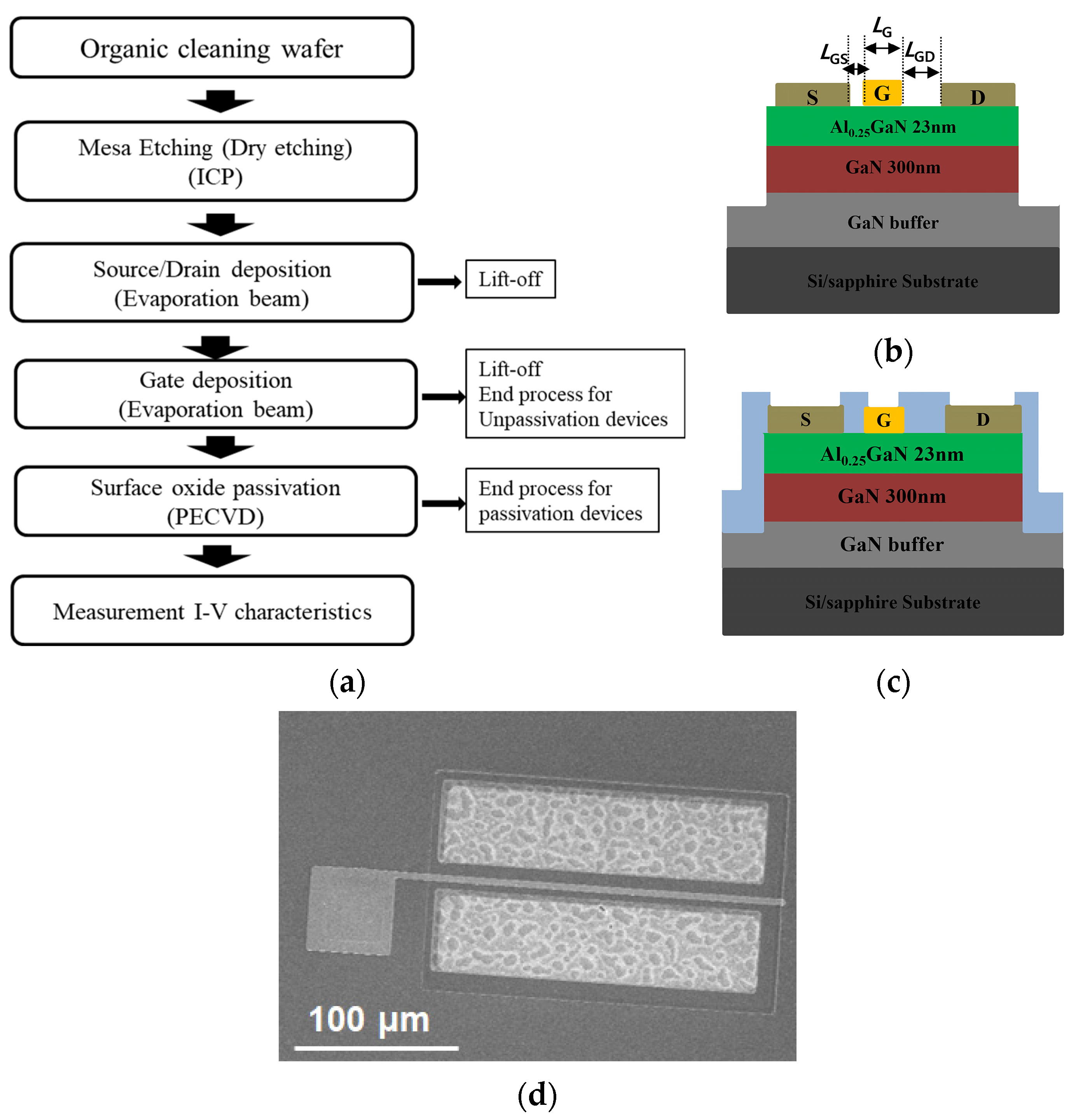
2. Materials and Methods

In this work, the metal organic chemical vapor deposition (MOCVD) grown epitaxial wafers on Si and sapphire substrates were purchased from Nippon Telegraph and Telephone Advanced Technology Co. (NNT-AT), Japan. The epitaxial wafers comprised, a 2-μm-thick GaN buffer layer with carbon-doping, a 300-nm-thick undoped GaN (i-GaN) layer, and a 23-nm-thick AlGaN barrier layer with aluminum composition of 25%. A 2DEG channel with an electron mobility of 1700 cm2/V-s and a sheet electron density of 1.1 × 1013 cm−2 was formed at the polarized AlGaN/GaN heterostructure interface. The choice of 25% aluminum, 300-nm-thick GaN channel, and 23-nm-AlGaN layer thickness are considered for the growth of AlGaN/GaN heterostructure to obtain high-performance AlGaN/GaN HEMTs through maintaining a trade-off between the on-current and the channel breakdown based on the 2DEG and the energy band gap. Further, the thickness of the layers is selected to obtain reduced deep traps, reduced threading dislocations, and reduced electron capture probability by the deep traps [31]. Both AlGaN/GaN HEMT device structures were processed under the same processing conditions, as exhibited in flow chart in Figure 1a. First, the wafers were cleaned using acetone followed by isopropyl alcohol for a duration of 3 min each. All cleanings were performed using ultrasonic agitation for the removal of organic contaminants from the surface. Later, the wafers were dipped in a H2SO4 + H2O2 (1:1) solution for 20 min and then in a buffer oxide etch (BOE) solution for 2 min. The cleaning procedure is an important step in preparing a surface for the formation of intimate electrode contact with the semiconductor. Mesa etching of the AlGaN/GaN layer was accomplished using an inductively coupled plasma (ICP) plasma-therm system defined by a photoresist hard mask with Ar/Cl2/BCl3 gas mixtures at an RF/bias power of 200/50 W and a chamber pressure of 3 mTorr. Ti/Al/Ni/Au (200/800/500/1000 Å) ohmic electrodes were formed as source and drain contacts by electron-beam evaporation tracked by rapid-thermal-annealing at 850 °C for 1 min in N2 flow. The sheet resistance and contact resistance values of 400.21 Ω/cm2 and 24.5 Ω, 666.84 Ω/cm2, and 20.97 Ω were obtained from the transmission line models (TLM) on Si and sapphire substrate, respectively. Finally, a Schottky gate contact was fabricated by the electron-beam evaporation of Ni/Au (200/1000 Å) films, defined by the pattern using standard UV lithography. To investigate the surface passivation effect using SiO2 on the AlGaN/GAN HEMT characteristics, a 200 nm thick SiO2 passivation layer was deposited on the fabricated HEMT structures via plasma-enhanced chemical vapor deposition. Prior to oxide passivation, the devices were cleaned by a BOE surface treatment for 1 min. The deposited SiO2 is sufficiently thick to create an electric field in the channel to reach the drain. Later, the source/drain and gate contact regions were opened by BOE etching. Schematics of the fabricated AlGaN/GaN structures with and without SiO2 passivation are exhibited in Figure 1b,c, respectively. The output and transfer characteristics of the fabricated AlGaN/GaN HEMTs were measured with a precision semiconductor parameter analyzer (Agilent 4156 C). The structural characterization of the AlGaN/GaN heterostructures grown on Si and sapphire substrates were performed employing high-resolution X-ray diffraction (HR-XRD, PANalytical X’ Pert Pro MRD). The root-mean-square surface roughness of the structures was measured by atomic force microscope (AFM; n-tracer, NanoFocus, Oberhausen, Germany).

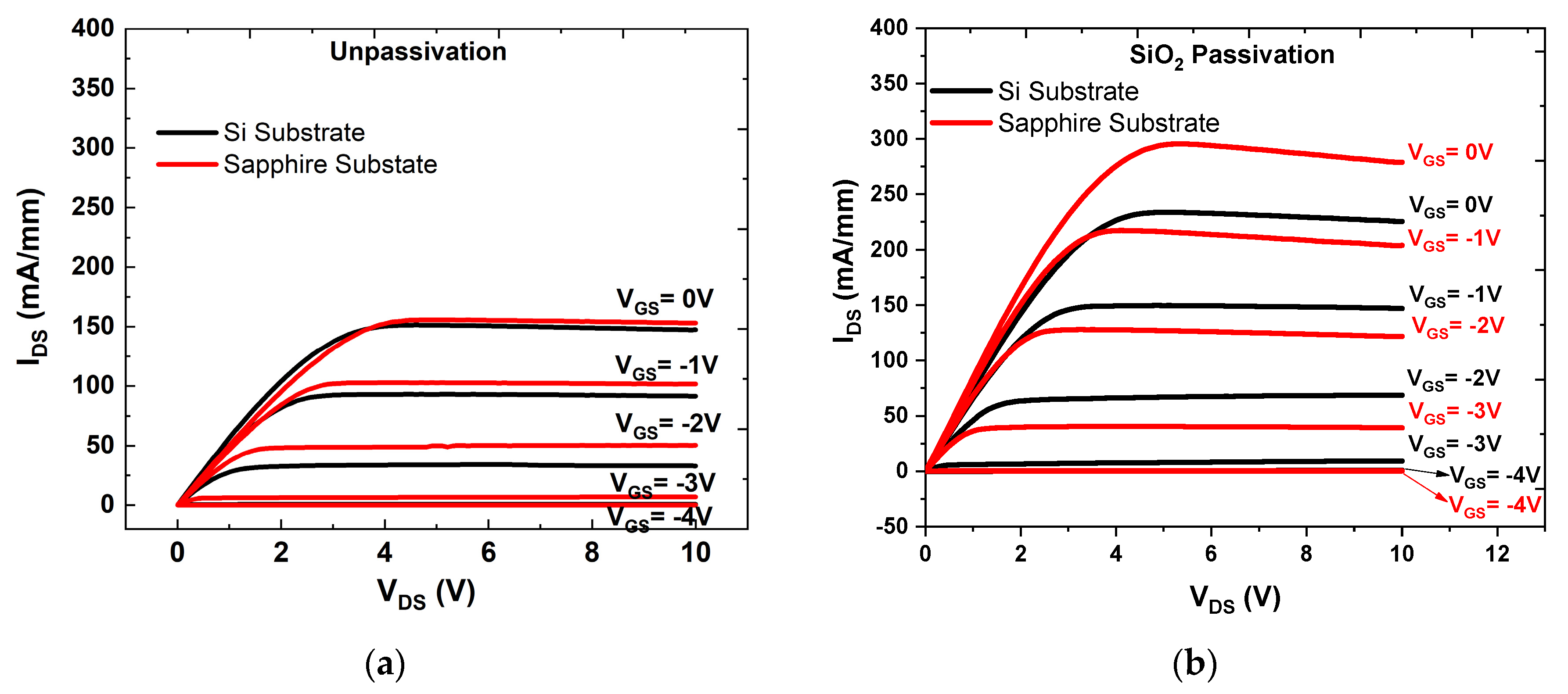
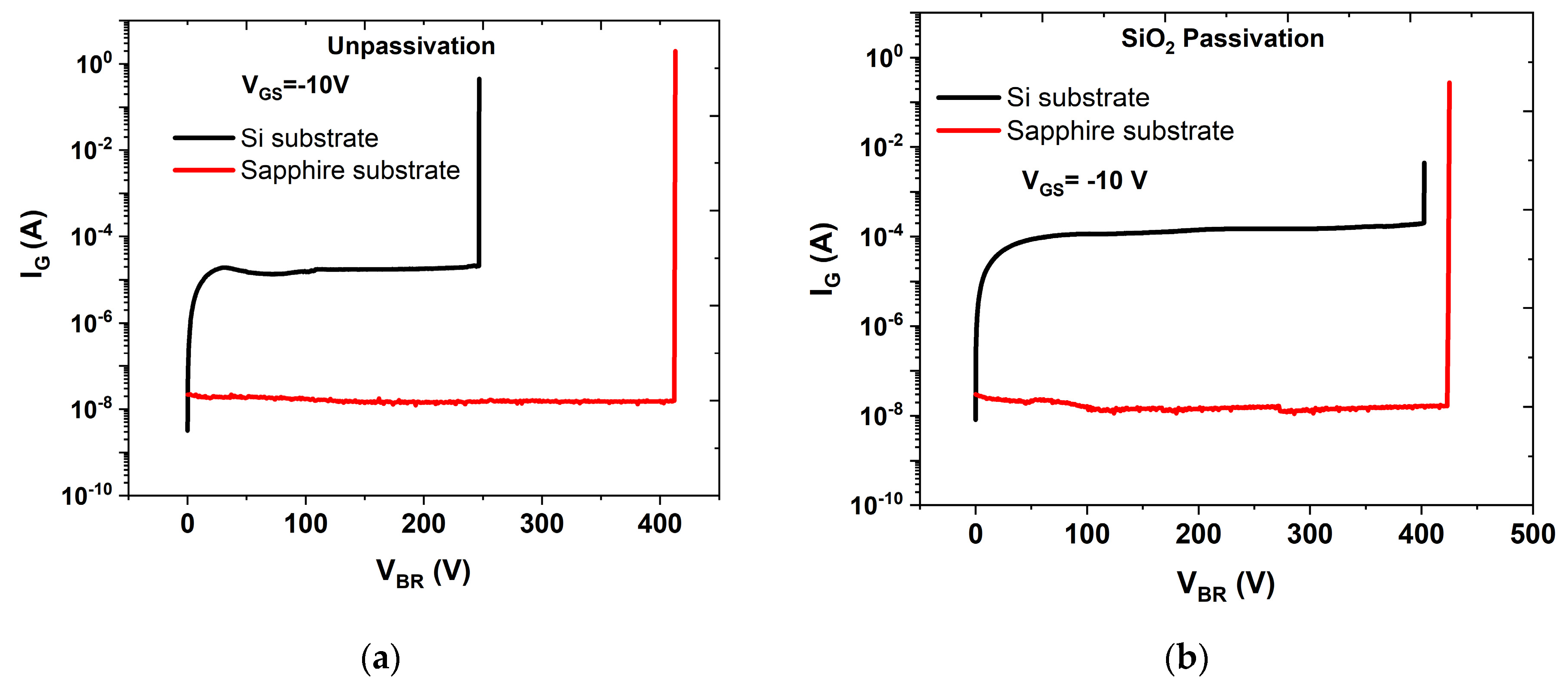
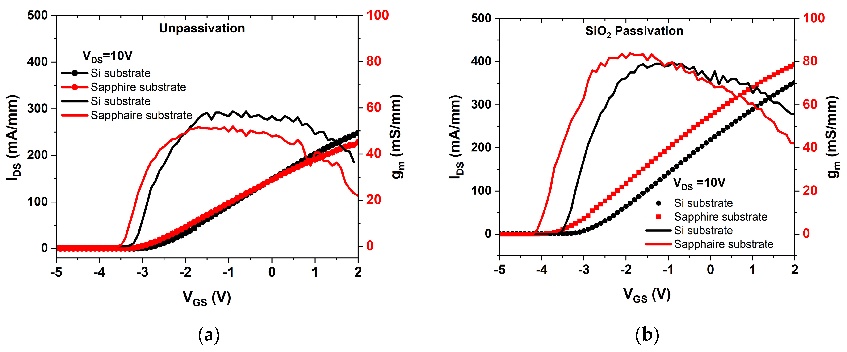
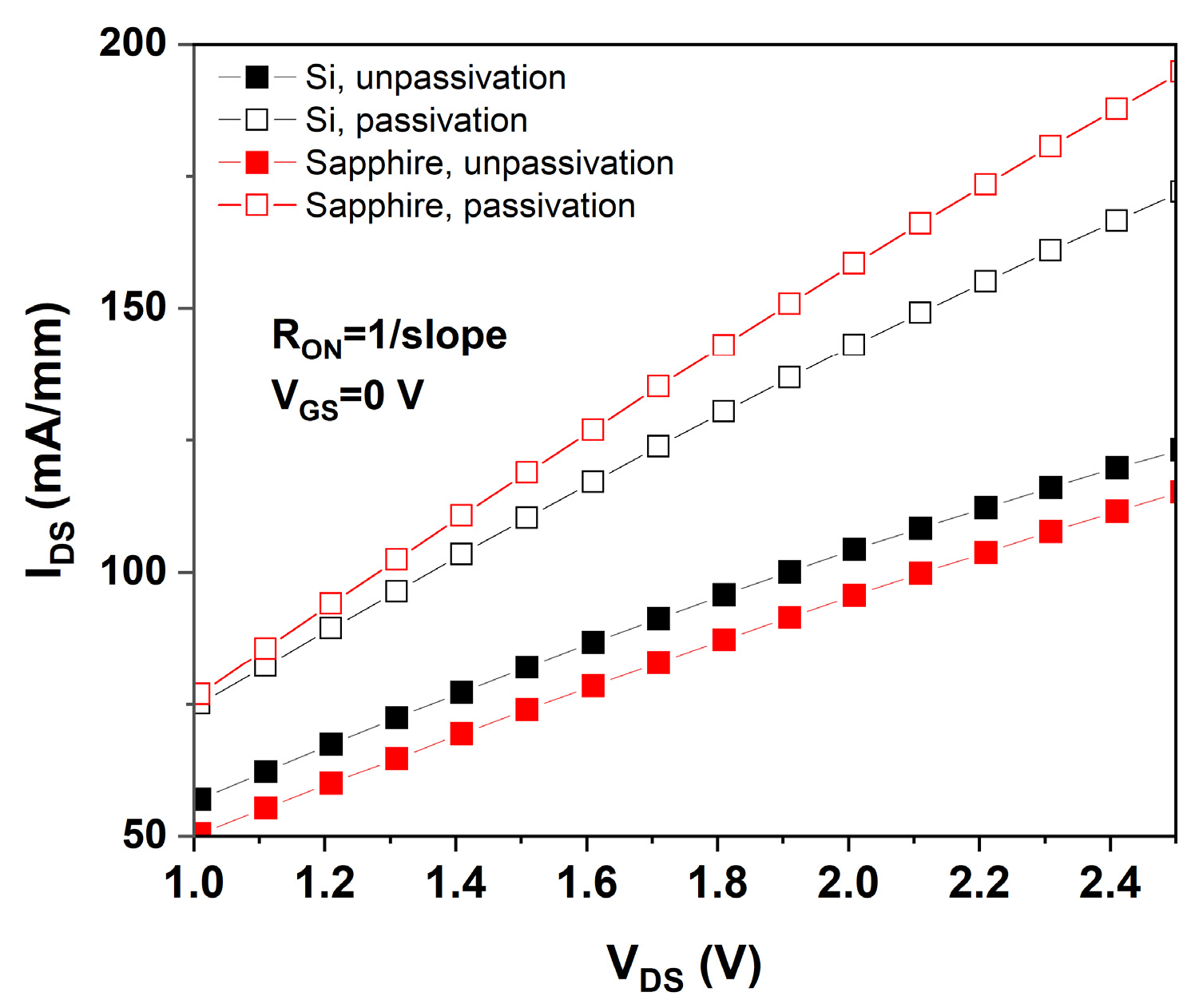
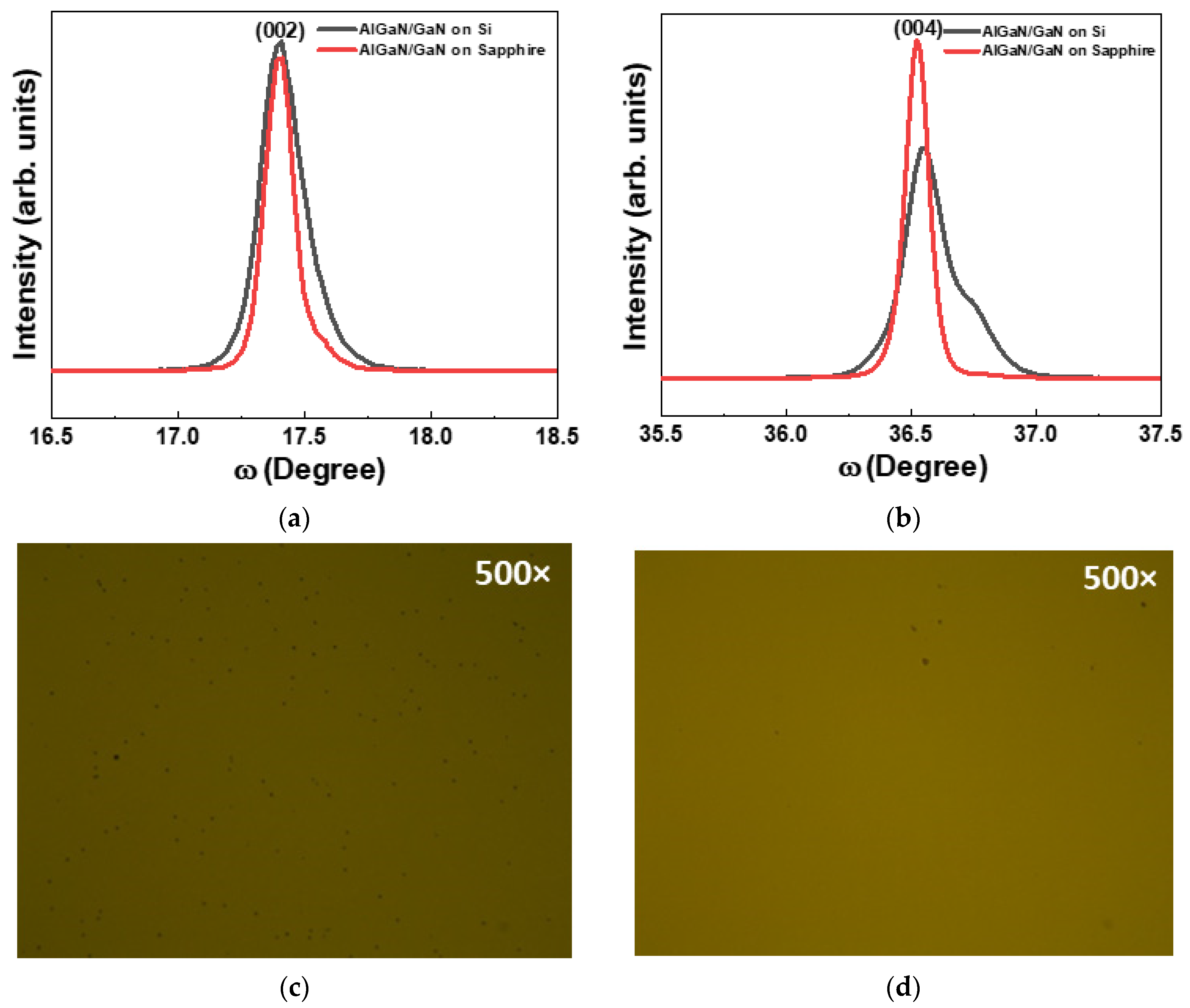
3. Results and Discussion

Figure 2a,b exhibit the output (IDS-VDS) curves of AlGaN/GaN HEMTs grown on Si and sapphire substrates at various VGS values varying in the range of –4 to 0 V with and without SiO2 passivation, respectively. The AlGaN/GaN HEMT grown on sapphire without any passivation shows better DC performance with a high drain current density of 155 mA/mm at VGS = 0 V than the HEMT grown on Si, which displayed a high drain current density of 150 mA/mm. However, the performance of the AlGaN/GaN HEMT fabricated on the passivated surfaces of both sapphire and Si substrates improved with drain current densities of 290 and 232 mA/mm at VGS = 0 V, respectively. The low drain current for low gate voltages (VGS) is associated with the reduced carriers in the heterojunction. The improvement in the drain currents after SiO2 passivation could be ascribed to the increase in the 2DEG charge and decrease in the electron injection to the surface traps [28]. Passivation decreases the surface effects that in turn augments the carriers in the channel leading to an increase in the drain current [32]. It can be noted that the drain current is higher for the AlGaN/GaN HEMTs fabricated on the sapphire than on the Si substrate that were identically processed and is mainly the effect of the substrates. Owing to the fact that both the devices have identical active layers, this higher drain current for the AlGaN/GaN HEMT on sapphire could be due to the better crystallinity than the Si sample that will be shown in the later sections [33]. The AlGaN/GaN HEMT fabricated on a passivated sapphire exhibited maximum values of IDS at VDS = 5 V and VGS = 0 V. It is to be noted that IDS decreased with increasing VDS owing to the self-heating effect of the sapphire because of its low thermal conductivity that limits the output power of the fabricated AlGaN/GaN HEMT [10,34,35]. Self-heating results in an increase in channel temperature that not only decreases the electron mobility and saturation velocity but also reduces the median time of power devices failure [35,36]. However, for AlGaN/GaN HEMT fabricated on passivated silicon, the decrease in IDS is negligible, implying a higher thermal conductivity of the Si than that of the sapphire substrate [10,34].
Figure 3a,b exhibit the breakdown voltage (VBR) curves of the AlGaN/GaN HEMTs fabricated on Si and sapphire substrates with and without SiO2 passivation, respectively. VBR is defined as VDS at IG = 1 mA at a gate bias VGS = –10 V. The drain-gate leakage current limits the VBR in these devices. For the AlGaN HEMTs fabricated on Si and sapphire substrates without any surface passivation, the VBR is obtained as 245 and 415 V, respectively, at corresponding gate leakage currents (IG) of 10 μA and 10 nA. The VBR values increased to 400 and 425 V after SiO2 passivation of the Si and sapphire substrates, respectively. The increase was owing to the decreased surface leakage current associated with electron injection suppression to the surface traps, implying the effectiveness of the SiO2 passivation [28]. It is worth noting that the VBR increased about 40% and by only 4%, respectively, for the AlGaN/GaN HEMTs fabricated on Si and sapphire substrates with SiO2 passivation. The VBR increased only slightly after SiO2 passivation for the AlGaN/GaN HEMT on sapphire substrate as compared with the one on Si that were processed identically. This slight increase in VBR could be due to the poorer thermal conductivity of sapphire. Self-heating happens as the applied power to the device produces heat that is not effectively conducted away letting the device to remain at the substrate’s ambient temperature. As the drain voltage is increased, the self-heating effects increases the device’s lattice temperature degrading the physical properties thus limiting the device VBR. As shown in Figure 3b, IG increased slightly after SiO2 passivation, particularly in the case of the HEMT fabricated on the Si substrate. This could be associated with the screening of traps, thereby enhancing the 2DEG [28,37].
Figure 4a,b exhibit the transfer and transconductance curves at VDS = 10 V for the AlGaN/GaN HEMTs fabricated on Si and sapphire substrates with and without SiO2 passivation. It is to be noted that the threshold voltage (Vth) decreases after oxide passivation with a shift towards the negative side from –3.0 to –3.5 V and from –3.0 to –3.8 V for the AlGaN/GaN HEMTs fabricated on Si and sapphire substrates, respectively. The decrease in Vth after SiO2 passivation could be due to reduction of electron trapping in the surface states [38,39]. Furthermore, from the figures, it can be noticed that a high transconductance (gm.max) of 50 and 58 mS/mm for the AlGaN/GaN HEMTs fabricated on Si and sapphire substrates increases to 80 and 86 mS/mm after SiO2 passivation, respectively, at VDS = 10 V. This increase in gm.max is associated with an increase in IDS. It can be noticed that the gm of the AlGaN/GaN HEMT on sapphire substrate is larger than that of the HEMT on Si for lower VGS till −2 and −0.9 V, respectively, for the HEMTS without and with SiO2 passivation at which the gm crosses each other. The behavior of gm changes after this crossing such that the gm of the AlGaN/GaN HEMT on sapphire is lower than the one fabricated on Si substrate. Further, the gm of the AlGaN/GaN HEMT decreases rapidly after this crossing particularly in the case of the HEMT fabricated on sapphire substrate owing to the self-heating effect as discussed earlier.
Figure 5 exhibits the linear output (IDS–VDS) curves of AlGaN/GaN HEMTs fabricated on Si and sapphire substrates with and without SiO2 passivation at VGS = 0 V, with which the dynamic resistance (RON) was determined. The RON reflects charge trapping in the material and is accredited to the interface trap states, barrier, surface, and buffer layer [40]. The values of RON are 4.44 and 4.33 Ω.mm for the AlGaN/GaN HEMTs fabricated on Si and sapphire substrates without SiO2 passivation and obtained as 0.64 Ω.mm and 1.26 Ω.mm for the HEMTs fabricated on SiO2 passivated surfaces. It was clearly observed that RON decreased after SiO2 passivation. This decrease in RON possibly indicates the effectiveness of the passivation and could be associated with the increase in the 2DEG and the suppression of electron injection into the surface traps [28].
The structural quality of the AlGaN/GaN epilayers grown on Si and sapphire substrates was investigated in the 2θ/ω scan mode using high-resolution X-ray diffraction (HR-XRD) to elucidate its effect on the device behavior of AlGaN/GaN HEMT. Figure 6a,b show the XRD ω -scan rocking curves of the (002) and (004) planes. The full width at half maximum (FWHM) values of the 002 and 004 diffraction peaks of AlGaN/GaN grown on both Si and sapphire substrates are presented in Table 1. From the measurements, the heterostructure deposited on the sapphire substrate exhibited good crystalline quality with a 002 reflection peak with an FWHM of 368 arcsec against an FWHM of 720 arcsec for the heterostructure grown on the Si substrate. The difference in the quality of the material depends mainly on the lattice mismatch and the crystal structure between the substrates and nitrides. In addition, the thermal expansion coefficient mismatch limits the material quality, resulting in residual strain with regard to epitaxy and dislocations [6,41]. Tensile stress is created in the heterostructures grown on Si and sapphire substrates owing to the variance in the thermal coefficients of the substrate materials and GaN. From the XRD results, it was noticed that the GaN grown on the sapphire substrate had a good crystalline quality. Figure 6c,d depict the optical force microscope images displaying the topography of the AlGaN/GaN epilayers grown on the Si and sapphire substrates. It is clearly observed from Figure 6c that the AlGaN epilayer grown on the Si substrate exhibits a large number of surface pits that may arise because of the threading dislocations intersection with the surface [1,42]. Furthermore, the surface topography of the GaN epilayers grown on Si and sapphire substrates was examined using atomic force microscopy (AFM) (Figures not shown here). A root-mean-square surface roughness of 2.96 and 0.88 nm is obtained from the AFM measurements for the GaN epilayers grown on Si and sapphire substrates, respectively, implying the GaN epilayer grown on sapphire exhibited a smooth surface. From the XRD and AFM results obtained, the AlGaN/GaN grown on the sapphire substrate exhibits better quality than that on a Si substrate owing to the larger lattice mismatch of GaN with Si compared with the sapphire substrate [41,43]. Lattice mismatch leads to high defect density and structural defects. Structural properties such as crystal quality, defects, and traps of the substrates affect the electrical properties of the fabricated devices. Owing to its better structural properties, the AlGaN/GaN HEMT grown on a sapphire substrate exhibited better electrical properties than those grown on a Si substrate.

4. Conclusions

The performance characteristics of the AlGaN/GaN HEMT structures fabricated on sapphire and Si substrates with and without SiO2 passivation were investigated. SiO2 passivation of the AlGaN/GaN HEMT led to an augmentation in the drain current IDS which could be attributed with an enhancement in the 2DEG charge and a decrease in the electron injection into the surface traps. The breakdown voltage of the HEMT increased on SiO2 passivation because of a reduction in the surface leakage current, indicating the effectiveness of SiO2 passivation. This implies that SiO2 passivation provides an effective approach for enhancing the electrical behavior of AlGaN/GaN HEMTs. The AlGaN/GaN HEMT device grown on a sapphire substrate displayed improved electrical performance compared with that grown on a Si substrate, which could be associated with the better crystallinity of the AlGaN/GaN heterostructure on sapphire. The outcomes of this work could indeed deliver an approach for the selection of the substrates for III-nitride epitaxial layers growth and surface passivation for the implementation of high performance AlGaN/GaN HEMTs on the basis.

Author Contributions

Conceptualization, S.P. and V.J.; methodology, S.P.; formal analysis, S.P., V.J. and T.-H.J.; writing—original draft preparation, S.P.; writing—review and editing, K.-H.S. and C.-J.C.; supervision, K.-H.S. and C.-J.C. All authors have read and agreed to the published version of the manuscript.

Funding

This research was supported by Korea Electric Power Corporation. (Grant number: R20XO02-10), and by Materials/Parts Technology Development Program (20022480) funded By the Ministry of Trade, Industry and Energy (MOTIE, Korea).

Data Availability Statement

No new data were created or analyzed in this study. Data sharing is not applicable to this article.

Conflicts of Interest

The authors declare no conflict of interest. The funding agencies had no role in the decision to publish the results.

References

  1. Kushvaha, S.S.; Pal, P.; Shukla, A.K.; Joshi, A.G.; Gupta, G.; Kumar, M.; Singh, S.; Gupta, B.K.; Haranath, D. Effect of growth temperature on defects in epitaxial GaN film grown by plasma assisted molecular beam epitaxy. AIP Adv. 2014, 4, 027114. [Google Scholar] [CrossRef]
  2. Qi, M.; Nomoto, K.; Zhu, M.; Hu, Z.; Zhao, Y.; Protasenko, V.; Song, B.; Yan, X.; Li, G.; Verma, J.; et al. High breakdown single-crystal GaN pn diodes by molecular beam epitaxy. Appl. Phys. Lett. 2015, 1072, 32101. [Google Scholar] [CrossRef] [Green Version]
  3. Alam, M.D.; Gaevski, M.; Jewel, M.U.; Mollah, S.; Mamun, A.; Hussain, K.; Floyd, R.; Simin, G.; Chandrashekhar, M.V.S.; Khan, A. Excimer laser liftoff of AlGaN/GaN HEMTs on thick AlN heat spreaders. Appl. Phys. Lett. 2021, 119, 132106. [Google Scholar] [CrossRef]
  4. Chen, H.; Tang, N.; Zuo, Z. Improvement and Reduction of Self-Heating Effect in AlGaN/GaN HEMT Devices. J. Sens. 2022, 10, 1–10. [Google Scholar] [CrossRef]
  5. Benzarti, Z.; Sekrafi, T.; Bougrioua, Z.; Khalfallah, A.; El Jani, B. Effect of SiN Treatment on Optical Properties of Inx Ga1− xN/GaN MQW Blue LEDs. J. Electron. Mater. 2017, 46, 4312–4320. [Google Scholar] [CrossRef]
  6. Wośko, M.; Paszkiewicz, B.; Szymański, T.; Paszkiewicz, R. Comparison of electrical, optical and structural properties of epitaxially grown HEMT’s type AlGaN/AlN/GaN heterostructures on Al2O3, Si and SiC substrates. Superlattices Microstruct. 2016, 100, 619–626. [Google Scholar] [CrossRef]
  7. Pharkphoumy, S.; Janardhanam, V.; Jang, T.H.; Park, J.; Shim, K.H.; Choi, C.J. Optimized Device Geometry of Normally-On Field-Plate AlGaN/GaN High Electron Mobility Transistors for High Breakdown Performance Using TCAD Simulation. Electronics 2021, 10, 2642. [Google Scholar] [CrossRef]
  8. He, X.G.; Zhao, D.G.; Jiang, D.S. Formation of two-dimensional electron gas at AlGaN/GaN heterostructure and the derivation of its sheet density expression. Chin. Phys. B 2015, 24, 067301. [Google Scholar] [CrossRef]
  9. Rathore, S.U.; Dimitrijev, S.; Amini Moghadam, H.; Mohd-Yasin, F. Equations for the electron density of the two-dimensional electron gas in realistic AlGaN/GaN heterostructures. Nanomanufacturing 2021, 1, 12. [Google Scholar] [CrossRef]
  10. Chang, S.J.; Cho, K.J.; Lee, S.Y.; Jeong, H.H.; Lee, J.H.; Jung, H.W.; Bae, S.B.; Choi, I.G.; Kim, H.C.; Ahn, H.K.; et al. Substrate Effects on the Electrical Properties in GaN-Based High Electron Mobility Transistors. Crystals 2021, 11, 1414. [Google Scholar] [CrossRef]
  11. Yusuf, Y.; Samsudin, M.E.A.; Taib, M.I.M.; Ahmad, M.A.; Mohamed, M.F.P.; Kawarada, H.; Falina, S.; Zainal, N.; Syamsul, M. Two-Step GaN Layer Growth for High-Voltage Lateral AlGaN/GaN HEMT. Crystals 2023, 13, 90. [Google Scholar] [CrossRef]
  12. Borga, M.; Meneghini, M.; Rossetto, I.; Stoffels, S.; Posthuma, N.; Van Hove, M.; Marcon, D.; Decoutere, S.; Meneghesso, G.; Zanoni, E. Evidence of time-dependent vertical breakdown in GaN-on-Si HEMTs. IEEE Trans. Electron Devices 2017, 64, 3616–3621. [Google Scholar] [CrossRef] [Green Version]
  13. Borga, M.; Meneghini, M.; Stoffels, S.; Van Hove, M.; Zhao, M.; Li, X.; Decoutere, S.; Zanoni, E.; Meneghesso, G. Impact of the substrate and buffer design on the performance of GaN on Si power HEMTs. Microelectron. Reliab. 2018, 88-90, 584–588. [Google Scholar] [CrossRef]
  14. Weyher, J.L.; Ashraf, H.; Hageman, P.R. Reduction of dislocation density in epitaxial GaN layers by overgrowth of defect-related etch pits. Appl. Phys. Lett. 2009, 95, 031913. [Google Scholar] [CrossRef]
  15. Halidou, I.; Benzarti, Z.; Bougrioua, Z.; Boufaden, T.; El Jani, B. Correlation between morphological, electrical and optical properties of GaN at all stages of MOVPE Si/N treatment growth. Superlattices Microstruct. 2006, 40, 490–495. [Google Scholar] [CrossRef]
  16. Boughrara, N.; Benzarti, Z.; Khalfallah, A.; Evaristo, M.; Cavaleiro, A. Comparative study on the nanomechanical behavior and physical properties influenced by the epitaxial growth mechanisms of GaN thin films. Appl. Surf. Sci. 2022, 579, 152188. [Google Scholar] [CrossRef]
  17. Wang, X.; Huang, S.; Zheng, Y.; Wei, K.; Chen, X.; Zhang, H.; Liu, X. Effect of GaN channel layer thickness on DC and RF performance of GaN HEMTs with composite AlGaN/GaN buffer. IEEE Trans. Electron Devices 2014, 61, 1341–1346. [Google Scholar] [CrossRef]
  18. Guan, H.; Shen, G.; Liu, S.; Jiang, C.; Wu, J. A Simulation Optimization Factor of Si (111)-Based AlGaN/GaN Epitaxy for High Frequency and Low-Voltage-Control High Electron Mobility Transistor Application. Micromachines 2023, 14, 168. [Google Scholar] [CrossRef]
  19. Singhal, J.; Chaudhuri, R.; Hickman, A.; Protasenko, V.; Xing, H.G.; Jena, D. Toward AlGaN channel HEMTs on AlN: Polarization-induced 2DEGs in AlN/AlGaN/AlN heterostructures. APL Mater. 2022, 10, 111120. [Google Scholar] [CrossRef]
  20. Green, B.M.; Chu, K.K.; Chumbes, E.M.; Smart, J.A.; Shealy, J.R.; Eastman, L.F. The effect of surface passivation on the microwave characteristics of undoped AlGaN/GaN HEMTs. IEEE Electron Device Lett. 2000, 21, 268–270. [Google Scholar] [CrossRef]
  21. Vetury, R.; Zhang, N.Q.; Keller, S.; Mishra, U.K. The impact of surface states on the DC and RF characteristics of AlGaN/GaN HFETs. IEEE Trans. Electron Devices 2001, 48, 560–566. [Google Scholar] [CrossRef]
  22. Adivarahan, V.; Simin, G.; Yang, J.W.; Lunev, A.; Khan, M.A.; Pala, N.; Shur, M.; Gaska, R. SiO2-passivated lateral-geometry GaN transparent Schottky-barrier detectors. Appl. Phys. Lett. 2000, 77, 863–865. [Google Scholar] [CrossRef] [Green Version]
  23. Xing, H.; Dora, Y.; Chini, A.; Heikman, S.; Keller, S.; Mishra, U.K. High breakdown voltage AlGaN-GaN HEMTs achieved by multiple field plates. IEEE Electron Device Lett. 2004, 25, 161–163. [Google Scholar] [CrossRef] [Green Version]
  24. Wang, W.K.; Lin, C.H.; Lin, P.C.; Lin, C.K.; Huang, F.H.; Chan, Y.J.; Chen, G.T.; Chyi, J.I. Low-/spl kappa/BCB passivation on AlGaN-GaN HEMT fabrication. IEEE Electron Device Lett. 2004, 25, 763–765. [Google Scholar] [CrossRef]
  25. Kang, M.J.; Kim, H.S.; Cha, H.Y.; Seo, K.S. Development of Catalytic-CVD SiNx Passivation Process for AlGaN/GaN-on-Si HEMTs. Crystals 2020, 10, 842. [Google Scholar] [CrossRef]
  26. Huang, C.Y.; Mazumder, S.; Lin, P.C.; Lee, K.W.; Wang, Y.H. Improved Electrical Characteristics of AlGaN/GaN High-Electron-Mobility Transistor with Al2O3/ZrO2 Stacked Gate Dielectrics. Materials 2022, 15, 6895. [Google Scholar] [CrossRef] [PubMed]
  27. Khan, M.A.; Hu, X.; Sumin, G.; Lunev, A.; Yang, J.; Gaska, R.; Shur, M.S. AlGaN/GaN metal oxide semiconductor heterostructure field effect transistor. IEEE Electron Device Lett. 2000, 21, 63–65. [Google Scholar] [CrossRef]
  28. Ha, M.W.; Lee, S.C.; Park, J.H.; Her, J.C.; Seo, K.S.; Han, M.K. Silicon dioxide passivation of AlGaN/GaN HEMTs for high breakdown voltage. In Proceedings of the 2006 IEEE International Symposium on Power Semiconductor Devices and IC’s, Naples, Italy, 4–8 June 2006; IEEE: Piscataway, NJ, USA, 2006; pp. 1–4. [Google Scholar] [CrossRef]
  29. Geng, K.; Chen, D.; Zhou, Q.; Wang, H. AlGaN/GaN MIS-HEMT with PECVD SiNx, SiON, SiO2 as gate dielectric and passivation layer. Electronics 2018, 7, 416. [Google Scholar] [CrossRef] [Green Version]
  30. Arulkumaran, S.; Egawa, T.; Ishikawa, H.; Jimbo, T.; Sano, Y. Surface passivation effects on AlGaN/GaN high-electron-mobility transistors with SiO2, Si3N4, and silicon oxynitride. Appl. Phys. Lett. 2004, 84, 613–615. [Google Scholar] [CrossRef]
  31. Boughrara, N.; Benzarti, Z.; Khalfallah, A.; Oliveira, J.C.; Evaristo, M.; Cavaleiro, A. Thickness-dependent physical and nanomechanical properties of AlxGa1−xN thin films. Mater. Sci. Semicond. Process. 2022, 151, 107023. [Google Scholar] [CrossRef]
  32. Gupta, A.; Chatterjee, N.; Kumar, P.; Pandey, S. Effect of surface passivation on the electrical characteristics of nanoscale AlGaN/GaN HEMT. IOP Conf. Ser. Mater. Sci. Eng. 2017, 225, 012095. [Google Scholar] [CrossRef]
  33. Mukhopadhyay, P.; Bag, A.; Gomes, U.; Banerjee, U.; Ghosh, S.; Kabi, S.; Chang, E.Y.; Dabiran, A.; Chow, P.; Biswas, D. Comparative DC characteristic analysis of AlGaN/GaN HEMTs grown on Si (111) and sapphire substrates by MBE. J. Electron. Mater. 2014, 43, 1263–1270. [Google Scholar] [CrossRef]
  34. Ji, H.; Das, J.; Germain, M.; Kuball, M. Laser lift-off transfer of AlGaN/GaN HEMTs from sapphire onto Si: A thermal perspective. Solid-State Electron. 2009, 53, 526–529. [Google Scholar] [CrossRef]
  35. Nigam, A.; Bhat, T.N.; Rajamani, S.; Dolmanan, S.B.; Tripathy, S.; Kumar, M. Effect of self-heating on electrical characteristics of AlGaN/GaN HEMT on Si (111) substrate. AIP Adv. 2017, 7, 085015. [Google Scholar] [CrossRef]
  36. Asubar, J.T.; Yatabe, Z.; Hashizume, T. Reduced thermal resistance in AlGaN/GaN multi-mesa-channel high electron mobility transistors. Appl. Phys. Lett. 2014, 105, 053510. [Google Scholar] [CrossRef] [Green Version]
  37. Song, L.; Fu, K.; Zhang, Z.; Sun, S.; Li, W.; Yu, G.; Hao, R.; Fan, Y.; Shi, W.; Cai, Y.; et al. Interface Si donor control to improve dynamic performance of AlGaN/GaN MIS-HEMTs. AIP Adv. 2017, 7, 125023. [Google Scholar] [CrossRef] [Green Version]
  38. Ha, M.W.; Choi, Y.H.; Park, J.H.; Seo, K.S.; Han, M.K. Hot Carrier Stress Effects of SiO2 Passivated AlGaN/GaN High Electron Mobility Transistors. ECS Trans. 2006, 3, 213–220. [Google Scholar] [CrossRef]
  39. Wu, Q.; Xu, Y.; Zhou, J.; Kong, Y.; Chen, T.; Wang, Y.; Lin, F.; Fu, Y.; Jia, Y.; Zhao, X.; et al. Performance comparison of GaN HEMTs on diamond and SiC substrates based on surface potential model. ECS J. Solid State Sci. Technol. 2017, 6, Q171–Q178. [Google Scholar] [CrossRef] [Green Version]
  40. Jin, D.; del Alamo, J.A. Mechanisms responsible for dynamic ON-resistance in GaN high-voltage HEMTs. In Proceedings of the 2012 24th International Symposium on Power Semiconductor Devices and ICs, Bruges, Belgium, 3–7 June 2012; pp. 333–336. [Google Scholar] [CrossRef]
  41. Ng, T.K.; Holguin-Lerma, J.A.; Kang, C.H.; Ashry, I.; Zhang, H.; Bucci, G.; Ooi, B.S. Group-III-nitride and halide-perovskite semiconductor gain media for amplified spontaneous emission and lasing applications. J. Phys. D Appl. Phys. 2021, 54, 143001. [Google Scholar] [CrossRef]
  42. Guillén-Cervantes, A.; Rivera-Álvarez, Z.; López-López, M.; Ponce-Pedraza, A.; Guarneros, C.; Sánchez-Reséndiz, V.M. Structural and optical properties of GaN thin films grown on Al2O3 substrates by MOCVD at different reactor pressures. Appl. Surf. Sci. 2011, 258, 1267–1271. [Google Scholar] [CrossRef]
  43. Liu, A.C.; Tu, P.T.; Langpoklakpam, C.; Huang, Y.W.; Chang, Y.T.; Tzou, A.J.; Hsu, L.H.; Lin, C.H.; Kuo, H.C.; Chang, E.Y. The evolution of manufacturing technology for GaN electronic devices. Micromachines 2021, 12, 737. [Google Scholar] [CrossRef] [PubMed]
Figure 1. (a) Flow chart showing the device fabrication process, schematic of the fabricated AlGaN/GaN HEMTs (b) without and (c) with SiO2 passivation, lengths are similar of LG S = 4μm, LG = 4.5 μm, and LGD = 10 μm, respectively, (d) scanning electron microscope image of the fabricated AlGaN/GaN HEMT structure.
Electronics 12 01049 g001
Figure 2. On-state IDS–VDS curves of AlGaN/GaN HEMTS on Si and sapphire substrates (a) without and (b) with SiO2 passivation.
Electronics 12 01049 g002
Figure 3. The off-state IGS-VDS curves of AlGaN/GaN HEMTs on Si and sapphire substrates (a) without and (b) with SiO2 passivation.
Electronics 12 01049 g003
Figure 4. The IDS-VGS transfer curves and transconductance curves of AlGaN/GaN HEMTs on Si and sapphire substrates (a) without and (b) with SiO2 passivation.
Electronics 12 01049 g004
Figure 5. Plot showing the linear regime of IDS versus VDS curves at VGS = 0 V for determining the dynamic on resistance of AlGaN/GaN HEMTs on Si and sapphire substrates without and with SiO2 passivation.
Electronics 12 01049 g005
Figure 6. ω-scan rocking curves of (a) (002) and (b) (004) planes, optical microscope images of AlGaN/GaN surface grown on (c) Si and (d) sapphire.
Electronics 12 01049 g006
Table 1. Parameters of the AlGaN/GaN grown on different substrates.
SubstratesRa
(nm)
HR-XRD
002 FWHM
(Degree)
HR-XRD
004 FWHM
(Degree)
XRC
002 FWHM
(Arcsec)
XRC
102 FWHM
(Arcsec)
AlGaN/GaN-on-Silicon2.960.200.237201312
AlGaN/GaN-on-sapphire0.880.130.12368647
Ra is roughness average.
Disclaimer/Publisher’s Note: The statements, opinions and data contained in all publications are solely those of the individual author(s) and contributor(s) and not of MDPI and/or the editor(s). MDPI and/or the editor(s) disclaim responsibility for any injury to people or property resulting from any ideas, methods, instructions or products referred to in the content.

