Article

Modified RPWM Strategy Based on Level-Shifted Random Carrier and Power Balance to Reduce the PWM Voltage Noise in Three-Phase CHB Inverters

1
School of Electrical Engineering, Guangxi University, Nanning 530004, China
2
School of Traffic &Transportation, Nanning University, Nanning 530200, China
*
Authors to whom correspondence should be addressed.
Electronics 2023, 12(3), 744; https://doi.org/10.3390/electronics12030744
Submission received: 29 December 2022 / Revised: 19 January 2023 / Accepted: 25 January 2023 / Published: 2 February 2023
(This article belongs to the Special Issue Power Electronics Converter Topologies and Control Techniques)

Abstract

:
Aimed at the pulse width modulation (PWM) voltage noise and power imbalance in three-phase cascaded H-Bridge (CHB) inverters, a modified random PWM (RPWM) strategy, named the power-balanced RPWM (PB-RPWM) strategy, is proposed in this paper. The PB-RPWM strategy mainly includes three steps: (1) random pulse signals are generated by compared modulation wave with level-shifted random carriers; (2) the random pulse signals are circularly distributed between CHB units by a logic operation method, and then the driving pulse signals of switching devices are produced; (3) the driving pulse signals are used to control the inverter. Under the PB-RPWM strategy, the spectra of the line voltage become uniform and continuous, that is, the PWM voltage noise of the line voltage can be effectively reduced. The output voltage of a single H-bridge unit can contain three basic voltages within 3/2 TA, that is, the power balance between CHB units can be realized. When compared with conventional non-random and random PWM strategies, the PB-RPWM strategy has a lower PWM voltage noise and smaller total harmonic distortion (THD). When compared with the level-shifted PWM (LS-PWM) strategy, the PB-RPWM strategy has a balanced power performance. The effectiveness and feasibility of the PB-RPWM strategy is verified by abundant simulations and experiments.

1. Introduction

In modern AC drive systems, PWM technology has been widely used with the continuous development of power electronics [1,2]. In three-phase inverters controlled by PWM technology, the line voltage contains PWM harmonic voltages related to the carrier frequency. These PWM harmonic voltages not only cause the waveform distortion of the line voltage, but also make the motor produce a harsh acoustic noise in AC drive systems [3]. Although raising the switching frequency to more than 15 kHz can avoid the hearing range of human ears, a high switching frequency reduces the efficiency of inverters [4]. When the switching frequency is low, the spectra of the line voltage can be continuous and uniform with RPWM strategies. This effectively reduces the peak value of the PWM voltage noise, so as to suppress the acoustic noise of the motor [5,6,7].
At present, CHB inverters has been widely used in medium and high voltage AC drive systems [8,9,10]. For H-bridge inverters, the current research focuses on how to reduce the PWM voltage noise in single H-bridge inverters. For example, an improved random SHE method was proposed to eliminate the specific PWM voltage noise in [11]. Taking random and non-random PS-PWM strategies as an example, the thermal impact of random and fixed switching frequency is studied in [12], which shows that the two switching modes have a similar thermal impact. The carrier sequences of phase-shifted random carriers in the RPWM strategies were researched in [13], which points out that optimized carrier sequences of phase-shifted random carriers help to further reduce the PWM voltage noise. These studies above improve the performance of the RPWM strategies based on a phase-shifted carrier from a random algorithm, carrier sequence and switching loss. Thus, these modified PS-RPWM strategies can effectively reduce the PWM voltage noise in single H-bridge inverters.
Generally, when compared with single H-bridge inverters, not only do CHB inverters have better waveform quality, but they are also more suitable for high voltage inverters [14,15]. When compared with the PS-PWM strategy, the LS-PWM strategy has a better waveform quality of the line voltage [16,17]. However, the RPWM strategies used for CHB inverters are very scarce at the moment, which will restrict the development of reducing the PWM voltage noise in H-bridge inverters. Therefore, in this paper the PB-RPWM strategy is proposed to further improve the waveform quality and reduce the PWM voltage noise in three-phase CHB inverters.
When compared with the studies above, this research does not optimize the RPWM strategies for single H-bridge inverters from a random algorithm and carrier sequence, but it optimizes the RPWM strategy for CHB inverters using a modulation strategy itself. Thus, the significant contribution of this study can be summarized with two points: (1) a RPWM strategy based on level-shifted random carrier is proposed for CHB inverters, which has a better performance of PWM voltage noise reduction; (2) a power balance method based on logic operation is proposed, which solves the power imbalance between cascaded H-bridge units.
In Section 2, the principle and implementation of the PB-RPWM strategy is introduced in detail. In Section 3, the characteristics and performances of the PB-RPWM strategy are analyzed through simulation and contrast. In Section 4, the effectiveness and feasibility of the PB-RPWM strategy is verified through an experimental platform of the three-phase CHB inverter.

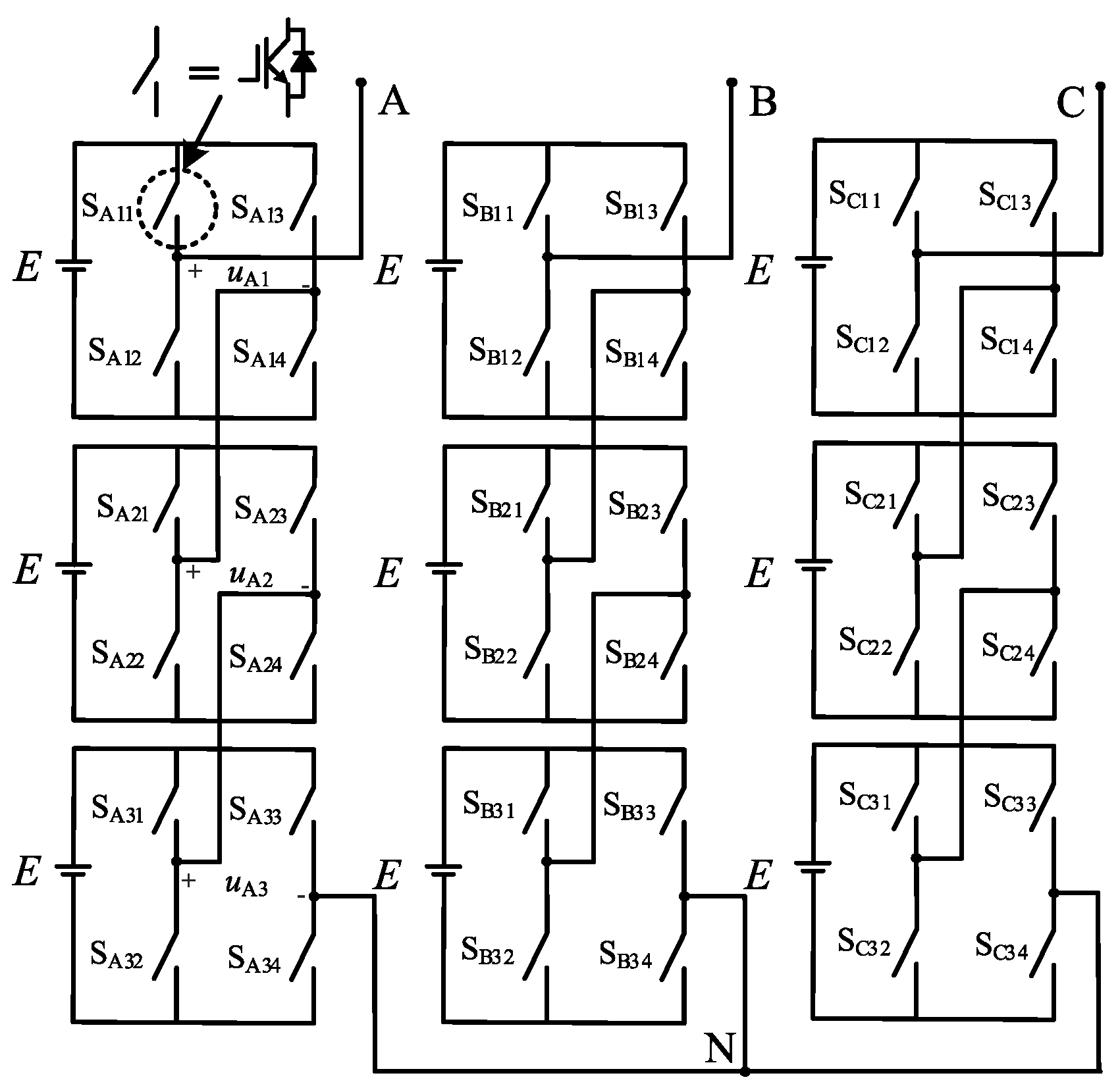
2. Introduction of the PB-RPWM Strategy

The topology of the three-phase CHB inverter is shown in Figure 1. From this figure, the single-phase inverter in this topology is composed of cascaded 3 H-bridge units. The principle and implementation of the PB-RPWM strategy is introduced by taking the A-phase CHB inverter as an example in this paper. Of course, the PB-RPWM strategy for the B-phase or C-phase CHB inverter can be obtained by replacing vA with vB or vC.

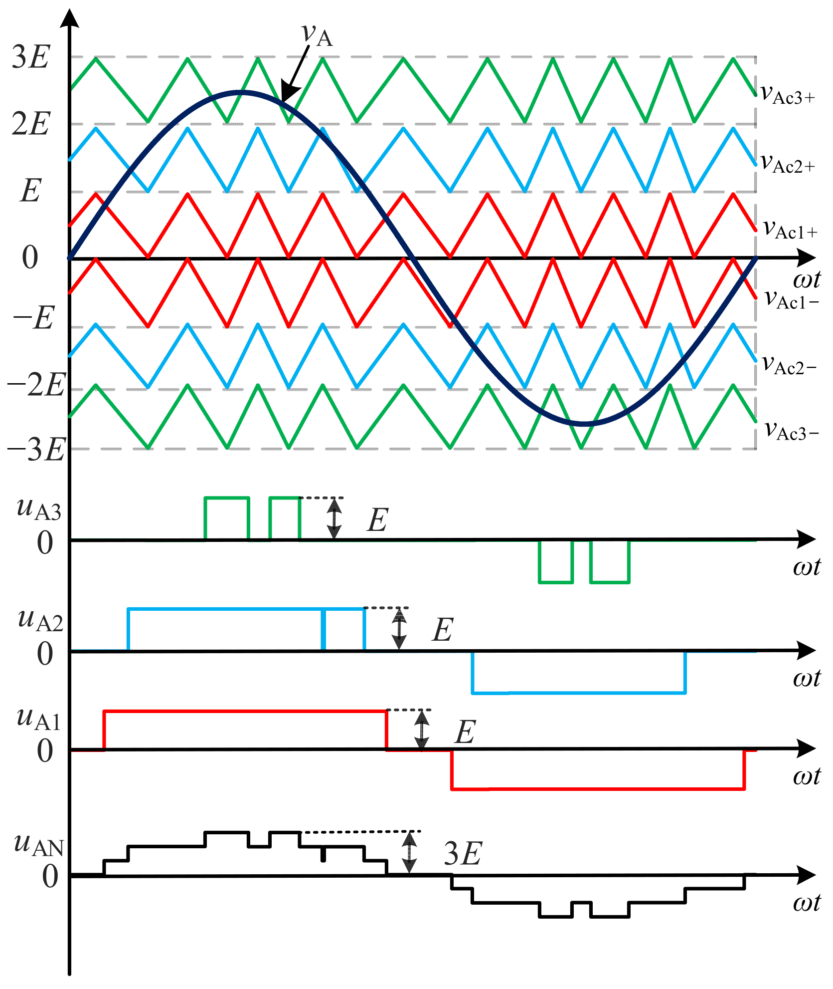
2.1. PWM Voltage Noise Reduction

In general, the LS-PWM strategy has smaller THD of the line voltage than the PS-PWM strategy. Accordingly, the LS-RPWM strategy based on a level-shifted random carrier is proposed as shown in Figure 2, which is expected to further reduce the THD and PWM voltage noise of the line voltage. In Figure 2, the random carriers of the cascaded H-bridge units A1, A2 and A3 are vAc1±, vAc2± and vAc3±, respectively. vAc1±, vAc2± and vAc3± are random carriers with the same frequency. The output voltage of the cascaded H-bridge units A1, A2 and A3 is uA1, uA2 and uA3, respectively. vA is the modulation wave of the A-phase CHB inverter, and uAN is the output voltage of the A-phase CHB inverter. The random pulse signals XA11 and XA13, XA21 and XA23, and XA31 and XA33 can be obtained by comparing vA with vAc1±, vAc2±, and vAc3±, respectively.
The random frequency fc of vAci± (i = 1, 2, 3) can be expressed as:
f c = f c 0 + R n Δ f
In (1), fc0 is the center frequency, and Δf is the bandwidth of random frequency, both of which are constants. The period of a random carrier is Tc = 1/fc. Rn is a random number in [−1, 1], which can be generated by uniform distribution random algorithms such as Logistic, Chebyshev, and Xorshift. vA can be expressed as:
v A ( t ) = 3 M a E sin ( ω A t )
Then, the average output voltage u ¯ Ai of uAi (i = 1, 2, 3) within Tc is
u ¯ A i = d i E v A 0 d i E v A < 0
In (4), di (i = 1, 2, 3) is the ratio between the output time of the H-bridge unit Ai and Tc, and its value range is in [0, 1]. In the positive period of uAN, when fc >> fA (fA = ωA/2π), di can be expressed as:
d i = 0 0 v A < ( 3 i ) E v A E ( 3 i ) ( 3 i ) E v A < ( 4 i ) E 1 ( 4 i ) E v A 3 E
According to (3) and (4), the average output voltage u ¯ AN within Tc can be expressed as:
u ¯ AN = i = 1 3 u ¯ A i = E i = 1 3 d i = v A
According to (5), under the LS-RPWM strategy, u ¯ AN within Tc is equal to the instantaneous value of vA. Similarly, the same conclusion can be obtained in a negative period of uAN.

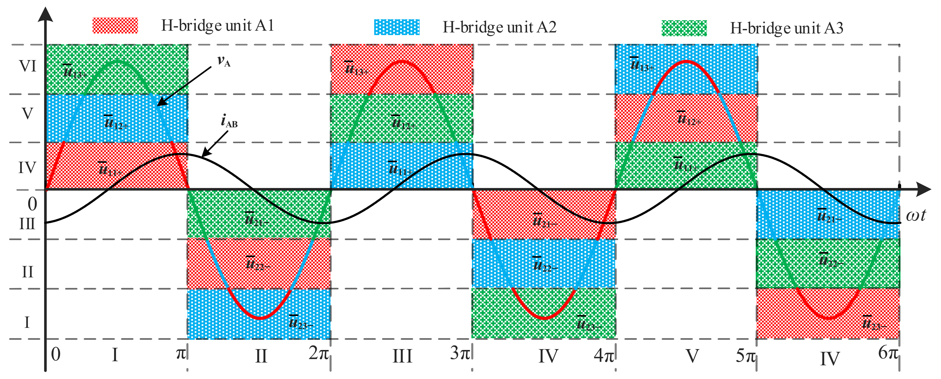
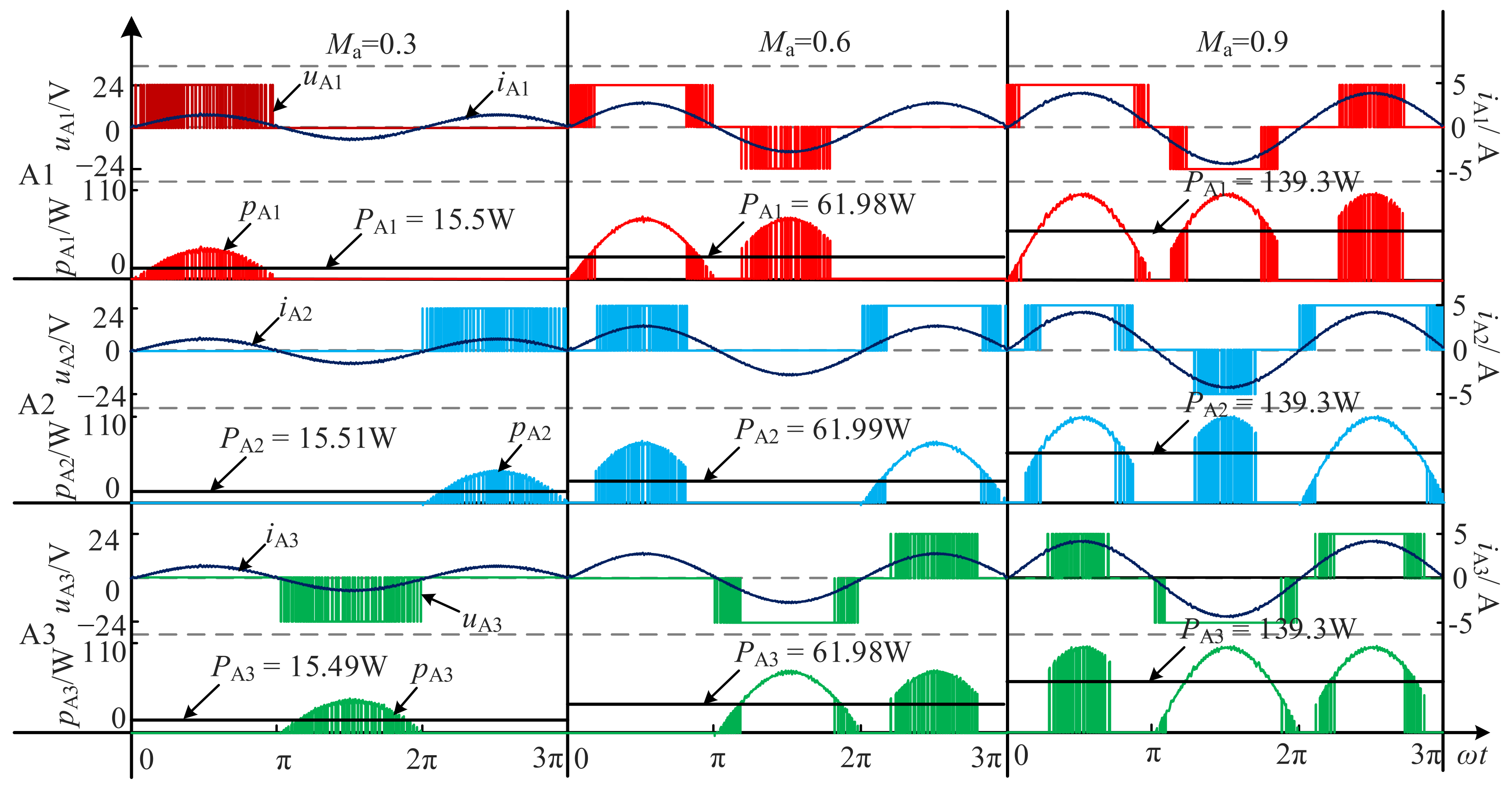
2.2. Power Balance Optimization

Under the proposed LS-RPWM strategy, when the power factor angle φ is 0 PAi/PA-Ma (i = 1, 2, 3), the curves are shown in Figure 3a, and when the modulation degree Ma is 0.85 PAi/EIA-φ (i = 1, 2, 3), the curves are shown in Figure 3b. In Figure 3, PA1, PA2 and PA3 is the average output power of the cascaded H-bridge units A1, A2, and A3, respectively, and PA is the average output power of the A-phase CHB inverter. From Figure 3a, PA1/PA, PA2/PA, and PA3/PA curves do not coincide with the power balance curve under any Ma. From Figure 3b, PA1/EIA, PA2/EIA, and PA3/EIA curves do not coincide with the power balance curve under any φ. This shows that average output power of the H-bridge units A1, A2 and A3 is not equal under any Ma and φ, that is, there is power imbalance between the cascaded H-bridge units A1, A2 and A3. The power imbalance leads to large differences in the utilization ratio of H-bridge units and DC voltage sources. These differences seriously reduce the reliability of the inverters and increase their maintenance cost [18,19,20]. Therefore, it is necessary to realize power balance between cascaded H-bridge units under the LS-RPWM strategy.
To facilitate the analysis of power distribution, vA within TA is divided to regions I and II, as shown in Figure 4. In region I, the comparison between vA and vAci+ (i = 1, 2, 3) can control the H-bridge unit Ai output basic voltage u ¯ A1i+. In region II, the comparison between vA and vAci− (i = 1, 2, 3) can control the H-bridge unit Ai output basic voltage u ¯ A2i. In regions I and II, u ¯ A1i+ and u ¯ A2 are the average output voltages of H-bridge unit Ai.
In region I, u ¯ A1i+ can be expressed as:
u ¯ A 11 + = 3 M a E sin ( ω t ) 0 ω t < β 1 E β 1 ω t < π β 1 3 M a E sin ( ω t ) π β 1 ω t π
u ¯ A 12 + = 0 0 ω t < β 1 3 M a E sin ( ω t ) E β 1 ω t < β 2 E β 2 ω t < π β 2 3 M a E sin ( ω t ) E π β 2 ω t < π β 0 π β 1 ω t π
u ¯ A 13 + = 0 0 ω t < β 2 3 M a E sin ( ω t ) 2 E β 2 ω t < π β 2 0 π β 2 ω t π
In region II, u ¯ A2i− can be expressed as:
u ¯ A 11 + = 3 M a E sin ( ω t ) 0 ω t < β 1 E β 1 ω t < π β 1 3 M a E sin ( ω t ) π β 1 ω t π
u ¯ A 12 + = 0 0 ω t < β 1 3 M a E sin ( ω t ) E β 1 ω t < β 2 E β 2 ω t < π β 2 3 M a E sin ( ω t ) E π β 2 ω t < π β 0 π β 1 ω t π
u ¯ A 13 + = 0 0 ω t < β 2 3 M a E sin ( ω t ) 2 E β 2 ω t < π β 2 0 π β 2 ω t π
In (6)–(11), β1 and β2 are, respectively:
β 1 = arcsin ( 1 3 M a ) β 2 = arcsin ( 2 3 M a )
Assuming iA is output current of the A-phase inverter, and its expression is:
i A = I A sin ( ω t φ )
In (13), IA is the current amplitude and φ is the power factor angle. Under basic voltage u ¯ Aji± (j = 1, 2; i = 1, 2, 3), the average output power PAji± can be expressed as:
P A j i ± = 1 π j π j π u ¯ j i ± i A d ( ω t )
According to (6), (13) and (14), PA11+ is:
P A 11 + = 1 π 0 π u ¯ 11 + i A d ( ω t ) = E I A cos ( φ ) π [ 2 cos ( β 1 ) 1.5 M a sin ( 2 β 1 ) + 3 M a β 1 ]
and PA21− is:
P A 21 = 1 π π 2 π u ¯ 21 i A d ( ω t ) = E I A cos ( φ ) π [ 2 cos ( β 1 ) 1.5 M a sin ( 2 β 1 ) + 3 M a β 1 ]
It can be seen from (15) and (16) that PA11+=PA21−. Similarly,
P A 12 + = P A 22 = E I A cos ( φ ) π [ 4 cos ( β 2 ) 2 cos ( β 1 ) + 1.5 M a sin ( 2 β 1 ) 1.5 M a sin ( 2 β 2 ) 3 M a β 1 + 3 M a β 2 ]
P A 13 + = P A 23 = E I A cos ( φ ) π [ 1.5 π M a 3 M a β 2 + 1.5 M a sin ( 2 β 2 ) 4 cos ( β 2 ) ]
From (16)–(18), PA11+ = PA21− under u ¯ A11+ and u ¯ A21−, PA12+ = PA22− under u ¯ A12+ and u ¯ A22−, and PA13+ = PA23− under u ¯ A13+ and u ¯ A23−. Therefore, the power balance can be realized as long as uAi (i = 1, 2, 3) contains three basic voltages ( u ¯ A11+ or u ¯ A21−, u ¯ A12+ or u ¯ A22−, u ¯ A13+ or u ¯ A23−) within 3/2 TA. According to above analysis, a logic operation method is proposed to realize power balance. Under this method, the driving pulse signals SA11, SA13, SA21, SA23, SA31 and SA33 are obtained by the logic operation between pulse signals L1, L2, L3, L4, L5 and L6, and random pulse signals XA11, XA13, XA21, XA23, XA31 and XA33. The logic operation method to obtain SA11, SA12, SA13 and SA14 of H-bridge unit A1 is shown in Figure 5. From this figure, the logic expressions of SA11, SA12, SA13 and SA14 in H-bridge unit A1 are:
S A 11 = X A 11 · L 1 + X A 31 · L 3 + X A 21 · L 5 S A 12 = S A 11 ¯ S A 13 = X A 23 · L 2 + X A 13 · L 4 + X A 33 · L 6 S A 14 = S A 13 ¯
Similarly, the logic expressions of SA21, SA22, SA23 and SA24 in H-bridge unit A2 are:
S A 21 = X A 21 · L 1 + X A 11 · L 3 + X A 31 · L 5 S A 22 = S A 21 ¯ S A 23 = X A 33 · L 2 + X A 23 · L 4 + X A 13 · L 6 S A 24 = S A 23 ¯
The logic expressions of SA31, SA32, SA33 and SA34 in H-bridge unit A3 are:
S A 31 = X A 31 · L 1 + X A 21 · L 3 + X A 11 · L 5 S A 32 = S A 31 ¯ S A 33 = X A 13 · L 2 + X A 33 · L 4 + X A 23 · L 6 S A 34 = S A 33 ¯
Under the driving pulse signals SAmn (m = 1, 2, 3; n = 1, 2, 3, 4), the contained basic voltages in uAi (i = 1, 2, 3) are shown in Figure 6. From this figure, in [0, 3π], uA1 contains the basic voltages u ¯ A11+, u ¯ A22− and u ¯ A13+, uA2 contains the basic voltages u ¯ A12+, u ¯ A23− and u ¯ A11+, and uA3 contains the basic voltages u ¯ A13+, u ¯ A21− and u ¯ A12+. According to the above analysis, in [0, 3π],
PA1 is:
P A 1 = P 11 + + P 22 + P 13 + = 1.5 M a E I A cos ( φ )
PA2 is:
P A 2 = P 12 + + P 23 + P 11 + = 1.5 M a E I A cos ( φ )
and PA3 is:
P A 3 = P 13 + + P 21 + P 12 + = 1.5 M a E I A cos ( φ )
Similarly, in [3π, 6π]:
P A 1 = P A 2 = P A 3 = 1.5 M a E I A cos ( φ )

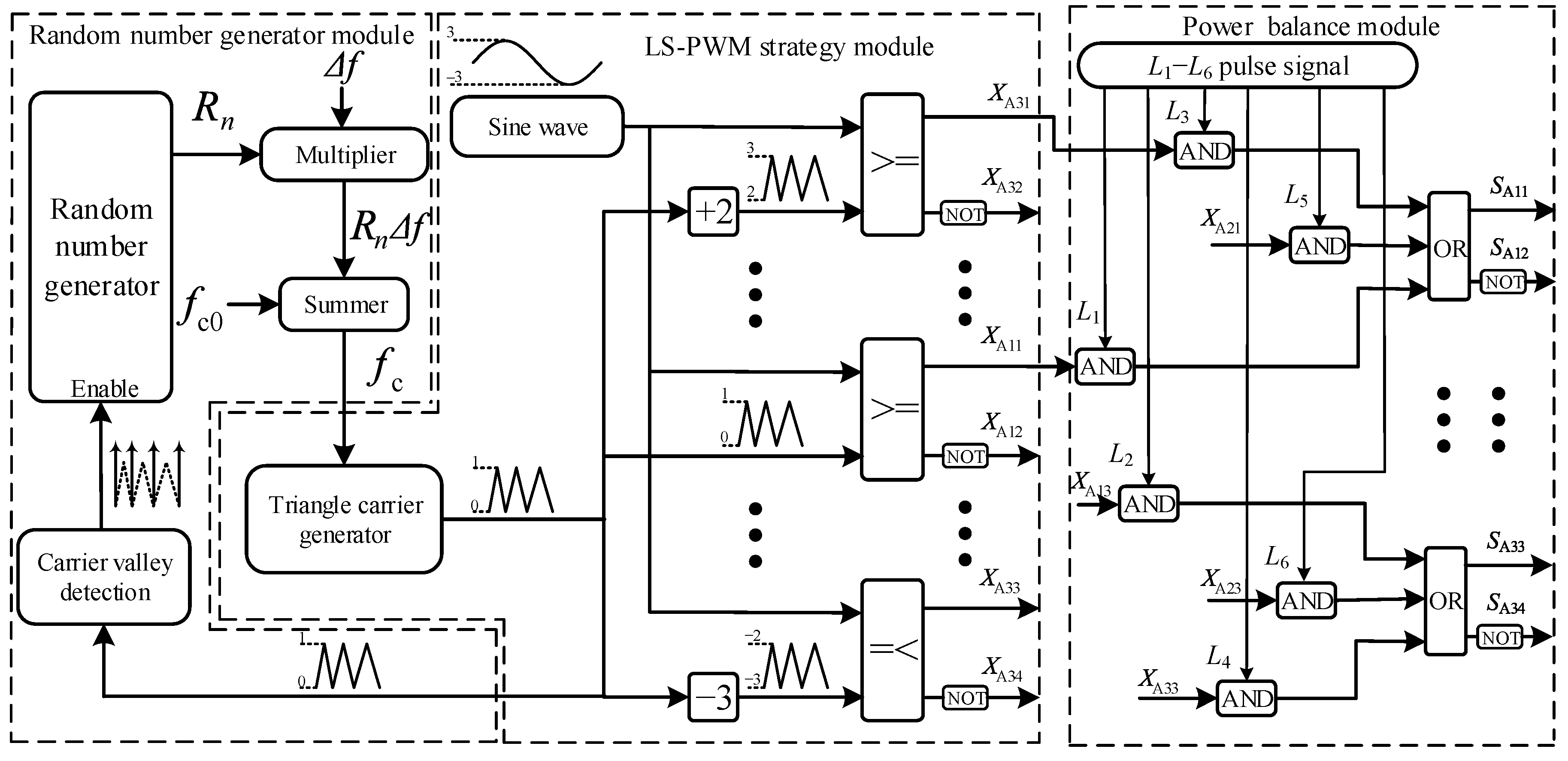
2.3. Digital Implementation of the PB-RPWM Strategy

The proposed PB-RPWM strategy can be obtained by combining the LS-RPWM strategy with the logic operation method, and its overall technical framework is shown in Figure 7. It can be seen that the PB-RPWM strategy only has a random number generator module and a power balance module when compared with the LS-PWM strategy. Therefore, the digital implementation of the PB-RPWM strategy is still very simple, and it can still be implemented by high performance microprocessors such as FPGA.
The digital implementation principle based on FPGA is shown in Figure 8. It can be seen that the principle based on FPGA mainly includes a phase-locked loop (PLL), random number generator, triangle carrier generator, sine function table, comparator, L1–L6 pulse signal generator, logic operation module and dead time module. These modules can be implemented in FPGA through Verilog HDL. It should be noted that Figure 8 is a general design framework based on Figure 2. Therefore, the amplitude of the sine wave and carrier wave in Figure 8 should be adjusted according to the actual situation. Generally, in order to avoid complex floating-point operations as much as possible, the amplitude of sine wave and carrier wave should be set to a larger integer, such as 255.
Specifically, (1) a 1 MHz clock signal can be generated through the PLL in FPGA. (2) The random number generator can be designed based on the Logistic or Xorshift random algorithm. When the random number generator receives the enable signal, the random algorithm iterates to generate a random number. (3) The carrier generators can be designed based on up-down counters. The carrier sequences with random frequency can be obtained using a random counting slope. (4) The sine function data generated through Matlab is stored in FPGA to construct the sine function table. When the sine function table receives the sampling signal, a sine value is output to the comparator. (5) In the comparator, the sine value is compared with the carrier to generate the random pulse signals XAmn (m = 1, 2, 3; n = 1, 2, 3, 4). (6) L1–L6 pulse signals can be generated by the fractional frequency of the clock signal. (7) In the logic operation module, the driving signals SAmn (m = 1, 2, 3; n = 1, 2, 3, 4) can be generated by the logic operation of XAmn and L1–L6. In practical application, it should be noted that the dead-time should be added to the driving signals SAmn.

3. Simulation and Contrast

A simulation model of the three-phase CHB inverter is built to analyze the characteristics and performances of the proposed PB-RPWM strategy, and its circuit parameters are shown in Table 1. In order to contrast under the same line voltage and average equivalent switching frequency, the different circuit parameters of the three-phase CHB inverter are set in Table 1. Specifically, the DC voltage source of a H-bridge unit is 72 V because these modulation strategies (RPWM-SHE [11], PS-RPWM [12] and PC-IRPWM [13]) are used for single H-bridge inverters. The DC voltage sources of H-bridge units are 24 V because these modulation strategies (PS-PWM [2], LS-PWM [19] and PB-RPWM) are used for cascaded 3 H-bridge inverters. The carrier frequency of the LS-PWM strategy is 6 kHz. The carrier frequency of the PS-PWM strategy is 1 kHz. The carrier frequency of the RPWM-SHE, PS-RPWM and PC-IRPWM strategies is 1.5~4.5 kHz. The carrier frequency of the PB-RPWM strategy is 3~9 kHz.

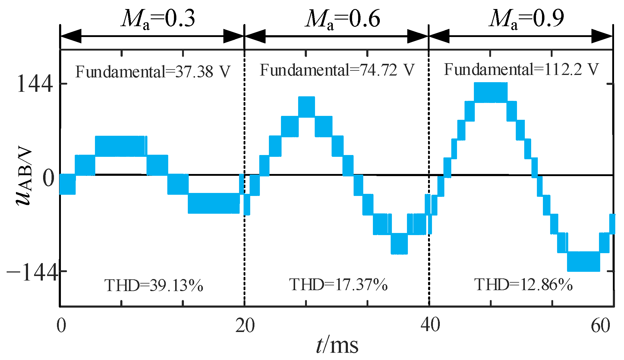
3.1. Characteristics of the PB-RPWM Strategy
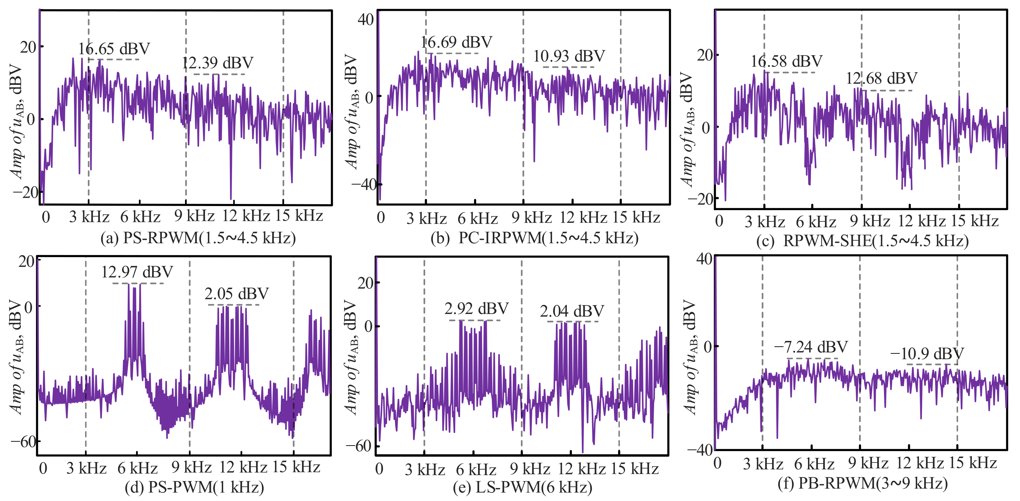
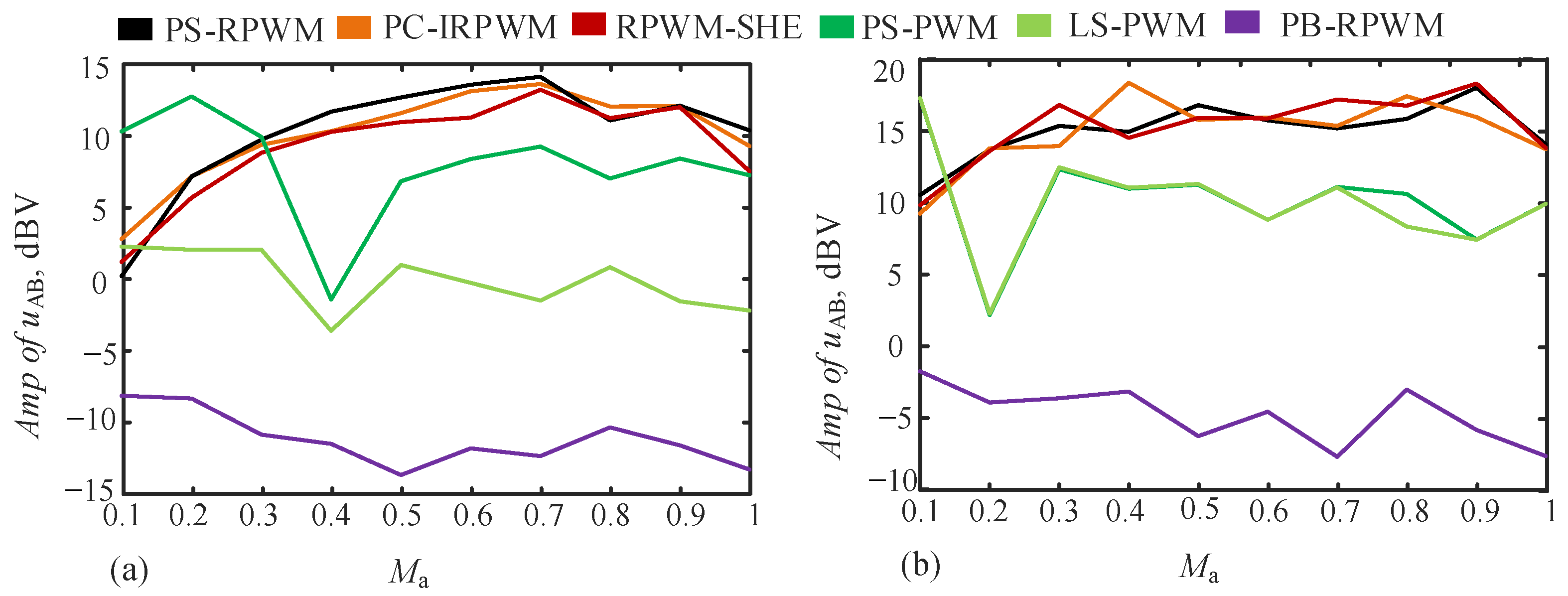
Under the PB-RPWM strategy, the simulation waveforms of the line voltage uAB are shown in Figure 9. From this Figure, when Ma is 0.3, 0.6 and 0.9, the levels of uAB are 5, 9 and 11, the THD of uAB is 39.13%, 17.37% and 12.86%, and the fundamental of uAB is 37.38 V, 74.72 V and 112.2 V, respectively. To sum up, the level, THD, and fundamental amplitude of the line voltage changes with Ma. When Ma increases, the level and fundamental of the line voltage is increased, and the THD of the line voltage is decreased.
Since the three-phase CHB inverter in this paper is symmetrical, the A-phase inverter is used as an example to show the power balance performance of the PB-RPWM strategy. When the load is RL (15 Ω–3 mH), simulation waveforms of output voltage uAi, output current iAi and output power pAi (i = 1, 2, 3) are shown in Figure 10. In this figure, uAi is the output voltage of H-bridge unit i (i = 1, 2, 3), iAi is the output current of H-bridge unit i and pAi is the output power of H-bridge unit i. From Figure 9, when Ma is 0.3, PA1 is 15.5 W, PA2 is 15.51 W and PA3 is 15.49 W. When Ma is 0.6, PA1 is 61.98 W, PA2 is 61.99 W and PA3 is 61.98 W. When Ma is 0.9, PA1 is 139.3 W, PA2 is 139.3 W and PA3 is 139.3 W. As can be seen, the average output power of the H-bridge units A1, A2, and A3 are basically equal in 3/2 TA. This indicates that the proposed PB-RPWM strategy can solve the power imbalance between the H-bridge units A1, A2, and A3. This will effectively balance the utilization ratio of H-bridge units and DC voltage sources, thereby improving the inverter’s reliability and reducing the inverter’s maintenance cost.

3.2. Contrast

When Ma = [0.1:0.1:1], the THD of the line voltage uAB under different modulation strategies is shown in Table 2. It can be seen that the PB-RPWM strategy has a significantly smaller THD of the line voltage when compared with the RPEM-SHE, PS-RPWM, PC-IRPWM and PS-PWM strategies. Simultaneously, the PB-RPWM strategy has almost the same THD of the line voltage when compared with the LS-PWM strategy. This shows that the PB-RPWM strategy has the same optimal harmonic performance of the line voltage as the LS-PWM strategy.
When Ma is 0.9, the spectra under different modulation strategies are shown in Figure 11. From this figure, under the PS-RPWM, PC-IRPWM, RPWM-SHE, PS-PWM, LS-PWM and PB-RPWM strategies, the 1st PWM voltage noise of uAB is 16.65 dBV, 16.69 dBV, 16.58 dBV, 12.97 dBV, 2.92 dBV and −7.24 dBV, and the 2nd PWM voltage noise of uAB is 12.39 dBV, 10.93 dBV, 12.68 dBV, 2.05 dBV, 2.04 dBV and −10.9 dBV, respectively. Furthermore, the 1st and 2nd PWM voltage noise when Ma = [0.1:0.1:1] are recorded. According to the obtained data, the Amp of uAB-Ma curves are drawn, as shown in Figure 12. It can be seen that the proposed PB-RPWM strategy has the minimum 1st and 2nd PWM voltage noises.
In order to better demonstrate the performance of PWM voltage noise reduction, the PWM voltage noise increment ΔdB1st,x and ΔdB2nd,x of the x (PC-IRPWM, RPWM-SHE, LS-PWM, and PB-RPWM) strategy is defined based on the 1st and 2nd PWM voltage noises of the PS-PWM strategy. The expressions of ΔdB1st,x and ΔdB2nd,x are:
Δ d B 1 st , x = d B 1 st , x d B 1 st , PS - PWM
Δ d B 2 nd , x = d B 2 nd , x d B 2 nd , PS PWM
In (26) and (27), dB1st,x and dB2nd,x are the 1st and 2nd PWM voltage noises of the x strategy, respectively. dB1st,PS-PWM and dB2nd,PS-PWM are the 1st and 2nd PWM voltage noises of the PS-PWM strategy, respectively.
Under different modulation strategies, ΔdB1st,x and ΔdB2nd,x are shown in Table 3. In this table, when Ma is 0.6, ΔdB1st,PB-RPWM and ΔdB2nd,PB-RPWM is −20.38 dBV and −13.05 dBV, that is, the PB-RPWM strategy can reduce the 1st and 2nd PWM voltage noise of the PS-PWM strategy by 20.38dBV and 13.05 dBV, respectively. Similarly, when Ma is 0.6, ΔdB1st,LS-PWM and ΔdB2nd,LS-PWM is −8.72 dBV and 0 dBV, that is, the LS-PWM strategy can reduce the 1st and 2nd PWM voltage noise of the PS-PWM strategy by 8.72 dBV and 0 dBV, respectively. Therefore, it can be seen that the proposed PB-RPWM has the best performance of PWM noise reduction when compared with the other modulation strategies above.
To sum up, not only can the proposed PB-RPWM reduce PWM voltage noise and the THD of the line voltage, but it can also realize a power balance between cascaded H-bridge units. In addition, the following two enlightenments can be obtained. First, CHB inverters obviously have z higher waveform quality and lower PWM voltage noise when compared with single H-bridge inverters. Second, RPWM strategies based on a level-shifted random carrier can further improve waveform quality and reduce PWM voltage noise when compared with RPWM strategies based on phase-shifted random carrier.

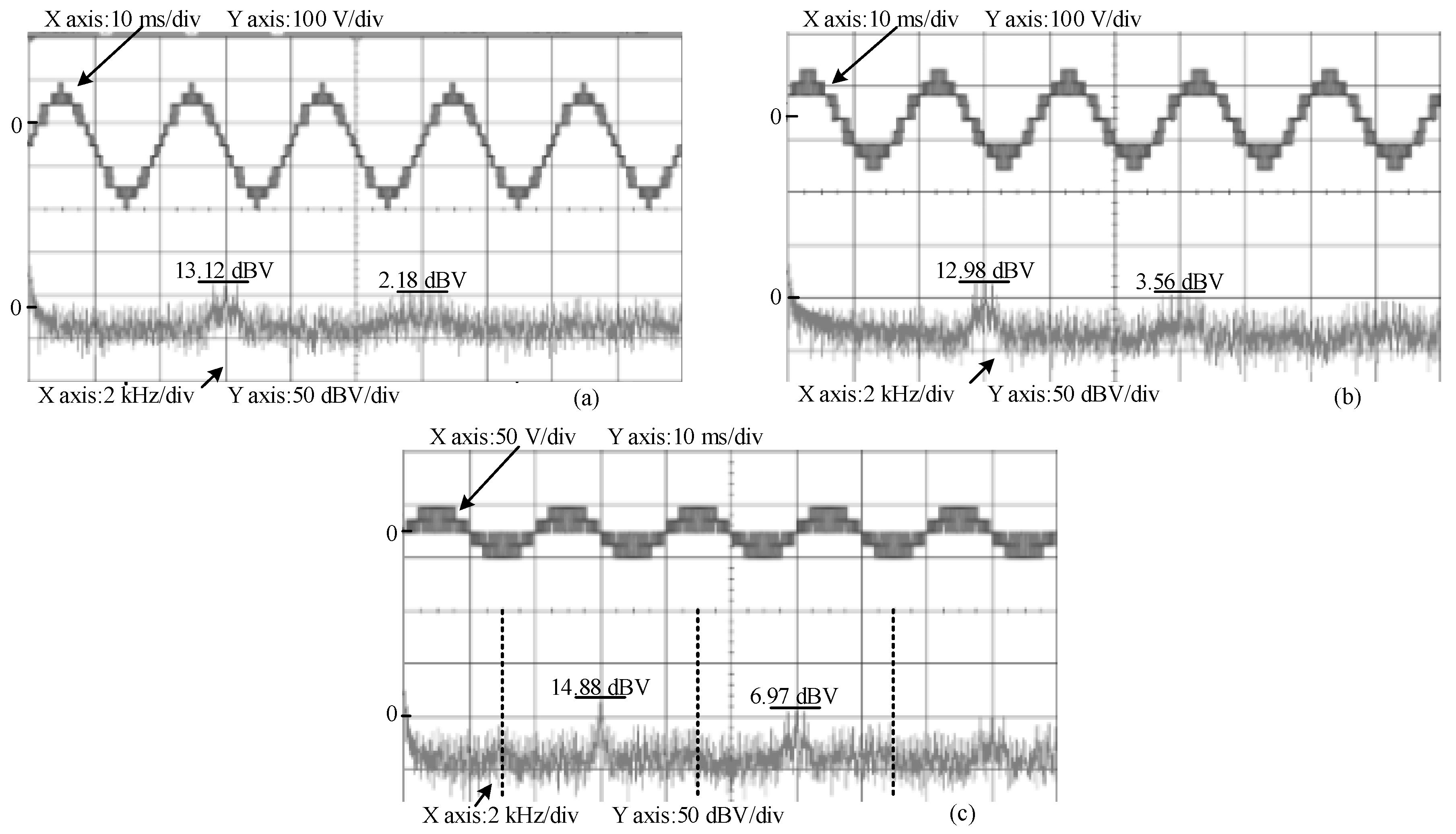
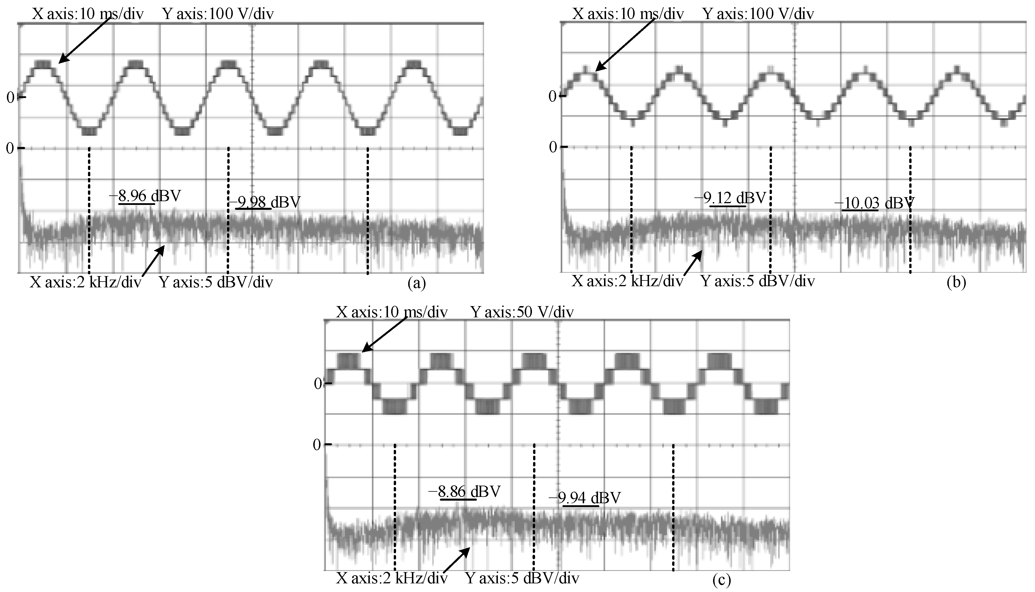
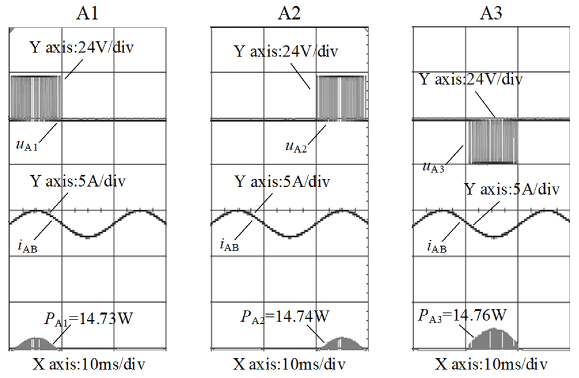
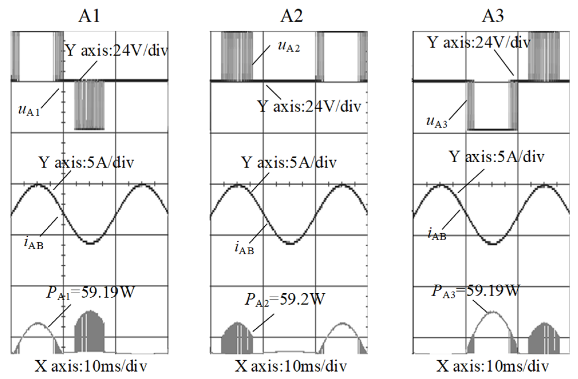
4. Experimental Verification

An experimental platform of the three-phase CHB inverter is built as shown in Figure 13 to further verify the effectiveness and feasibility of the PB-RPWM strategy, and its circuit parameters are shown in Table 1. Under the PS-PWM strategy, the experimental waveforms and spectra of the line voltage uAB are shown in Figure 14. From this figure, when Ma is 0.9, 0.6 and 0.3, the 1st PWM voltage noise is 13.12 dBV, 12.98 dBV and 14.88 dBV, and the 2nd PWM noise is 2.18 dBV, 3.56 dBV and 6.97 dBV, respectively. Under the PB-RPWM strategy, the experimental waveforms and spectra of the line voltage uAB are shown in Figure 15. From this figure, when Ma is 0.9, 0.6 and 0.3, the 1st PWM voltage noise is −8.96 dBV, −9.12 dBV and −8.86 dBV, and the 2nd PWM noise is −9.98 dBV, −10.03 dBV and −9.94 dBV, respectively. According to these data, when Ma is 0.9, 0.6 and 0.3, ΔdB1st,PB-RPWM is −22.08 dBV, −22.10 dBV and −23.74 dBV, and ΔdB2nd,PB-RPWM is −12.16 dBV, −13.59 dBV and −16.91 dBV, respectively. It can be seen that the performance of PWM voltage noise reduction in the experimental platform is basically consistent with it in the simulation model. This verifies the superior performance of the proposed PB-RPWM strategy in reducing PWM voltage noise of the line voltage.
When the load is RL (15 Ω–3 mH), the experimental waveforms of output voltage uAi, output current iAi and output power pAi (i = 1, 2, 3) are shown in Figure 16, Figure 17 and Figure 18. In Figure 16, when Ma is 0.3, PA1, PA2 and PA3 are 14.73 W, 14.74 W, and 14.76 W, respectively. In Figure 17, when Ma is 0.6, PA1, PA2, and PA3 are 59.19 W, 59.20 W, and 59.19 W, respectively. In Figure 18, when Ma is 0.9, PA1, PA2, and PA3 are 135.40 W, 135.39 W, and 135.40 W, respectively. It can be seen that the average output power of the H-bridge units A1, A2 and A3 are basically the same. Thus, the proposed PB-RPWM strategy can effectively realize the power balance between the cascaded H-bridge units A1, A2 and A3.

5. Conclusions

In this paper, the PB-RPWM strategy is proposed to reduce the PWM voltage noise of the line voltage and improve the power distribution between cascade H-bridge units in three-phase CHB inverters. The level-shifted carrier, random carrier frequency, and power balance are combined using the proposed level-shifted random carrier and logic operation method in this strategy. Thus, the PB-RPWM strategy not only has the optimal harmonic performance of the line voltage, but it can also reduce the PWM voltage noise of the line voltage and realize a power balance between cascaded H-bridge units. In addition, CHB inverters naturally have a better waveform quality and lower PWM voltage noise when compared with single H-bridge inverters. Therefore, CHB topologies and RPWM strategies based on a level-shifted random carrier and power balance can be given priority to obtain higher waveform quality and lower PWM voltage noise. The simulation and experimental results strongly verify the effectiveness and feasibility of the proposed PB-RPWM strategy.

Author Contributions

Conceptualization, J.L. and R.G.; methodology, J.L.; validation, J.L. and Y.Z.; writing—original draft preparation, J.L.; writing—review and editing, J.L., R.G. and Y.Z.; project administration, R.G.; funding acquisition, R.G. All authors have read and agreed to the published version of the manuscript.

Funding

This research was funded by the National Natural Science Foundation of China, grant number 61561007, and the Natural Science Foundation of Guangxi Province, China, grant number 2017GXNSFAA198168.

Data Availability Statement

The data used to support the findings of the study are available within the article.

Conflicts of Interest

The authors declare that they have no conflict of interest.

References

  1. Liu, S.; Liu, C. Virtual-vector-based robust predictive current control for dual three-phase PMSM. IEEE Trans. Ind. Electron. 2021, 68, 2048–2058. [Google Scholar] [CrossRef]
  2. Zhang, W.; Xu, Y.; Huang, H.; Zou, J. Vibration reduction for dual-branch three-phase permanent magnet synchronous motor with carrier phase-shift technique. IEEE Trans. Power Electron. 2020, 35, 607–618. [Google Scholar] [CrossRef]
  3. Lee, K.; Shen, G.; Yao, W.; Lu, Z. Performance characterization of random pulse width modulation algorithms in industrial and commercial adjustable-speed drives. IEEE Trans. Ind. Appl. 2017, 53, 1078–1108. [Google Scholar] [CrossRef]
  4. Kumar, A.B.C.; Narayanan, G. Variable-switching frequency PWM technique for induction motor drive to spread acoustic noise spectrum with reduced current ripple. IEEE Trans. Ind. Appl. 2016, 52, 3927–3938. [Google Scholar] [CrossRef]
  5. Lin, F.; Zuo, S.; Deng, W.; Wu, S. Modeling and analysis of electromagnetic force, vibration, and noise in permanent-magnet synchronous motor considering current harmonics. IEEE Trans. Ind. Electron. 2016, 63, 7455–7466. [Google Scholar] [CrossRef]
  6. Dove, A.; Naude, J.; Hofajer, I. An argument for the relationship between spectral spreading and probability spreading for EMI-reduction in DC–DC converter. IEEE Trans. Power Electron. 2020, 35, 1459–1472. [Google Scholar] [CrossRef]
  7. Kirlin, R.L.; Bech, M.M.; Trzynadlowski, A.M. Analysis of power and power spectral density in PWM inverters with randomized switching frequency. IEEE Trans. Ind. Electron. 2002, 49, 486–499. [Google Scholar] [CrossRef]
  8. Deng, W.; Zou, S. Electromagnetic vibration and noise of the permanent-magnet synchronous motors for electric vehicles: An overview. IEEE Trans. Transport. Electrific. 2019, 5, 59–70. [Google Scholar] [CrossRef]
  9. Kouro, S.; Malinowski, M.; Gopakumar, K.; Pou, J.; Franquelo, L.G.; Wu, B.; Rodriguez, J.; Perez, M.A.; Leon, J.I. Recent advances and industrial applications of multilevel converters. IEEE Trans. Ind. Electron. 2010, 57, 2553–2580. [Google Scholar] [CrossRef]
  10. Abu-Rub, H.; Holtz, J.J.; Rodriguez, J.; Baoming, G. Medium-voltage multilevel converters-state of the art challenges and requirements in industrial applications. IEEE Trans. Ind. Electron. 2010, 57, 2581–2596. [Google Scholar] [CrossRef]
  11. Li, G.; Liu, C.; Wang, Y. A novel RPWN selective harmonic elimination method for single-phase inverter. Electronics 2020, 9, 489. [Google Scholar] [CrossRef]
  12. Li, H.; Yang, Z.; Wang, B.; Agelidis, V.G.; Zhang, B. On thermal impact of chaotic frequency modulation SPWM techniques. IEEE Trans. Ind. Electron. 2017, 64, 2032–2043. [Google Scholar] [CrossRef]
  13. Xiong, J.; Li, R.; Wang, T.; Gao, J. Improved random PWM modulation method based on preset carrier switching frequency. J. Intell. Fuzzy Syst. 2020, 38, 311–318. [Google Scholar] [CrossRef]
  14. Hu, W.; Liu, J. A new scheme of hybrid H-bridge cascaded inverter. Proc. CSEE 2019, 39, 6044–6055. [Google Scholar]
  15. Adam, G.P.; Abdelsalam, I.A.; Ahmed, K.H.; Williams, B.W. Hybrid multilevel converter with cascaded H-bridge cells for HVDC applications: Operating principle and scalability. IEEE Trans. Power Electron. 2015, 30, 65–77. [Google Scholar] [CrossRef]
  16. Guo, X.; Wang, X.; Wang, C.; Lu, Z.; Hua, C.; Blaabjerg, F. Improved modulation strategy for singe-phase cascaded H-bridge multilevel inverter. IEEE Trans. Power Electron. 2022, 37, 2470–2474. [Google Scholar] [CrossRef]
  17. Meraj, M.; Rahman, S.; Iqbal, A.; Ben-Brahim, L.; Abu-Rub, H. Novel level shifted PWM technique for equal power sharing among quasi Z source modules in cascaded multilevel inverter. IEEE Trans. Power Electron. 2022, 36, 4766–4777. [Google Scholar] [CrossRef]
  18. Ye, M.; Peng, R.; Tong, Z.; Chen, Z.; Miao, Z. A generalized scheme with linear power balance and uniform switching loss for asymmetric cascaded H-bridge multilevel inverters. IEEE Trans. Power Electron. 2022, 37, 2719–2730. [Google Scholar] [CrossRef]
  19. Chen, Z.; Xu, Y.; Na, X.; Sun, J. Power balance control and optimization methods with output voltage rotation for cascaded multilevel inverter. Proc. CSEE 2018, 38, 1132–1142. [Google Scholar]
  20. Lopez-Santos, O.; Jacanamejoy-Jamioy, C.A.; Salazar-D’Antonio, D.F.; Corredor-ramirez, J.R.; Garcia, G.; Martinez-Salamero, L. A single-phase transformer-based cascaded asymmetric multilevel inverter with balanced power distribution. IEEE Access. 2019, 7, 98182–98196. [Google Scholar] [CrossRef]
Figure 1. Topology of the three-phase CHB inverter.
Electronics 12 00744 g001
Figure 2. Proposed the LS-RPWM strategy.
Electronics 12 00744 g002
Figure 3. Power curves: (a) PAi/PA-Ma (i = 1, 2, 3) curves at φ=0; (b) PAi/EIA-φ (i = 1, 2, 3) curves at Ma = 0.85.
Electronics 12 00744 g003
Figure 4. Basic voltages u ¯ A1i+ and u ¯ A2i.
Electronics 12 00744 g004
Figure 5. Logic operation method to obtain SA11, SA12, SA13 and SA14 of H-bridge unit A1.
Electronics 12 00744 g005
Figure 6. uAi (i = 1, 2, 3) contains basic voltages under driving pulse signals.
Electronics 12 00744 g006
Figure 7. Overall technical framework of the PB-RPWM strategy.
Electronics 12 00744 g007
Figure 8. Digital implementation principle based on FPGA.
Electronics 12 00744 g008
Figure 9. Simulation waveforms of uAB.
Electronics 12 00744 g009
Figure 10. Simulation waveforms of output voltage uAi, output current iAi and output power pAi.
Electronics 12 00744 g010
Figure 11. PWM voltage noise of uAB under different modulation strategies when Ma = 0.9.
Electronics 12 00744 g011
Figure 12. Comparison of PWM voltage noise: (a) 1st PWM voltage noise; (b) 2nd PWM voltage noise.
Electronics 12 00744 g012
Figure 13. Photograph of the experimental platform.
Electronics 12 00744 g013
Figure 14. Experimental waveforms and spectra under the PS-PWM strategy: (a) Ma = 0.9; (b) Ma = 0.6; (c) Ma = 0.3.
Electronics 12 00744 g014
Figure 15. Experimental waveforms and spectra under the PB-RPWM strategy: (a) Ma = 0.9; (b) Ma = 0.6; (c) Ma = 0.3.
Electronics 12 00744 g015
Figure 16. Experimental waveforms of uAi, iAi and pAi for Ma = 0.3.
Electronics 12 00744 g016
Figure 17. Experimental waveforms of uAi, iAi and pAi for Ma = 0.6.
Electronics 12 00744 g017
Figure 18. Experimental waveforms of uAi, iAi and pAi for Ma = 0.9.
Electronics 12 00744 g018
Table 1. Circuit parameters of the simulation and experimental.
ParameterValue
DC voltage1 H-bridge72 V
3 H-bridge24 V
Carrier frequencyPS1.5–4.5 kHz
LS3–9 kHz
Output frequency50 Hz
Three-phase LoadR = 15 ΩL = 3 mH
Table 2. THD of line voltage uAB under different modulation strategies.
Ma0.10.20.30.40.50.60.70.80.91
PS-RPWM3.692.521.981.641.391.201.050.9140.7960.685
PC-IRPWM3.722.521.981.631.391.211.050.9160.7970.687
RPWM-SHE3.712.521.981.641.391.201.050.9170.7960.685
PS-PWM1.700.9670.5380.2580.2920.2870.2400.1980.1830.150
LS-PWM1.210.4930.3920.2550.2340.1740.1660.1320.1280.107
PB-RPWM1.200.4930.3910.2550.2330.1740.1660.1330.1290.107
Table 3. ΔdB1st,x and ΔdB2nd,x under different modulation strategies.
Max0.10.20.30.40.50.60.70.80.91
dB1st,x/dBVPS-PWM14.8817.3414.53.0411.3812.9313.8111.5612.9711.80
ΔdB1st,x/dBVPS-RPWM−7.58−5.64−0.5711.874.784.784.415.083.682.06
PC-IRPWM−10.19−5.63−0.1913.245.895.234.924.093.723.15
RPWM-SHE−9.20−7.12−1.1211.814.152.914.004.253.610.28
LS-PWM−8.1−10.8−7.95−2.19−5.9−8.72−10.85−6.24−10.05−9.53
PB-RPWM−18.63−21.28−20.99−10.16−20.70−20.38−21.80−17.53−20.21−20.73
dB2nd,x/dBVPS-PWM11.66−3.086.845.525.783.405.645.172.054.49
ΔdB2nd,x/dBVPS-RPWM−6.5611.262.953.865.426.763.985.1010.344.04
PC-IRPWM−7.8311.351.577.214.416.964.146.638.343.73
RPWM-SHE−7.2611.164.373.464.556.895.955.9910.633.79
LS-PWM0.010100.140.060.060−0.04−2.24−0.010
PB-RPWM−18.56−5.94−15.59−13.80−17.10−13.05−18.36−13.31−12.95−17.17
Disclaimer/Publisher’s Note: The statements, opinions and data contained in all publications are solely those of the individual author(s) and contributor(s) and not of MDPI and/or the editor(s). MDPI and/or the editor(s) disclaim responsibility for any injury to people or property resulting from any ideas, methods, instructions or products referred to in the content.

